
Figure 1: simpleCPU games console
The aim of the simpleCPU teaching processor is that students learn through hands-on experience what a processor is by building one. Therefore, this is a journey from AND-gate to computer, leaving no stone unturned, the incremental refinement of the simpleCPU processor's architecture from version 1a to version 1d. The end goal of this journey being a DIY games console, because as we all know the true reason why computers were invented was to play video games :). Therefore, this web page hopefully pulls together all the existing work into a programming resource, a guide to how to write your own games running on the simpleCPU.
Stuff already made ...
Console - Version 1.0
Console - Version 1.1
Software
Games
Simulator

Figure 2: top level block diagram v1.0
To state the obvious to create a video games console we need a controller to capture the users inputs / commands, a processor to process these inputs, perform the games logic and create the output graphics, that will be displayed to the user. Fortunately, a number of these key hardware and software components have already been implemented:

Figure 3: games console - version 1.0
The first version of the simpleCPU games console (Video) uses an old Xilinx spartan 3E development board. For more technical details on this board: (Link) and for more information about the FGPA used: (Link). The two main reasons why i selected this board were that it has a built in VGA interface (just the connector and resistor based DAC) and we had a big box full of them spare (from an old module we no longer teach). Free is good :). The game consoles case is made from laser cut 3mm acrylic sheet, as shown in figure 4. The DXF files can be downloaded here: (Link). Note, at this time some of the push buttons on the FPGA board are not accessible. It is intended that push rods / buttons will be 3D printed later, if i remember :).

Figure 4: top and bottom panels
The simpleCPU logo and SNES connector box were 3D printed. Note, the logo was generated from a 2D image, imported into Inkscape, then using the Path -> Trace Bitmap tool, the bitmap image is converted into a vector image, that can then be saved as an "AutoCAD DXF R12" file. This DXF file can then be imported into openSCAD using the following commands and combined with other 3D elements. The DXF,SCAD and STL files can be downloaded here: (Link).
$fn=100;
hull(){
    translate([5,20,0]) cylinder(h=2, r=40/2);
    translate([55,20,0]) cylinder(h=2, r=40/2);
}
color("red") scale([2,2,1.25]) translate([-12,-39.5,0]) linear_extrude(height = 4) import("drawing-1a.dxf");
Figure 5: logo
The SNES controller plugs into a 3D printed box, well its hot glued into a 3D printed box, as the SNES socket is proprietary, a Nintendo specific connector which can not be easily obtained. Therefore, electrical connection to these pins are made using solid copper wires, cut to size such that they form a friction fit. These "plug pins" are then soldered to seven-strand copper wire, which in turn plugs into an IO header on the FPGA board. Discussion of the SNES interface controller running in the FPGA can be found here: (Link). The SCAD file can be downloaded here: (Link).


Figure 6: SNES controller box

Figure 7: top level architecture
The initial architecture used by this version of the games console is the same as that used in the space invaders demo (Link), shown in figure 7. I decided for the moment to keep the processor's clock speed at 10MHz to ensure stability. However, the synthesis tools do indicate that this design can run a lot faster, as shown in figure 8. Therefore, the system clock in later versions of the games console will be increased to 25MHz - 50MHz.

Figure 8: synthesis report
The core peripheral devices in this version of the games console are an: UART, GPIO, Rotary encoder, SNES and VGA. The memory map used in this architecture is shown in figure 9. Note, this memory mapped was changed in version 1.1.
ADDR      A1 A0 CS       WR                        RD

0xFFF     1  1  0        UART_TX                   UART_RX
0xFFE     1  0  0        UART_TX                   UART_STATUS

0xFFD     0  1  1        GPIO A out                GPIO A out
0xFFC     0  0  1        GPIO A out                GPIO A in

0xFFB     0  1  2        NU                        NU
0xFFA     1  0  2        ROTARY_RESET              ROTARY_DATA
0xFF9     0  1  3        SNES_DATA                 NU
0xFF8     0  0  3        SNES_START                SNES_STATUS

0xFF7     1  1  6        VGA                       VGA
0xFF6     1  0  6        VGA TILE_Y_REG
0xFF5     0  1  6        VGA TILE_X_REG
0xFF4     0  0  6        VGA CPU_DST_ADDR_REG
0xFF3     1  1  6        VGA CPU_COLOUR_REG        VGA TILE_POS
0xFF2     1  0  6        VGA CPU_DATA_IN_REG       VGA CPU_DATA_OUT_REG
0xFF1     0  1  6        VGA CPU_SRC_ADDR_REG
0xFF0     0  0  6        VGA CPU_CTL_REG           VGA CPU_STATUS_REG

0xFEF     1  1  MEM      RAM                       RAM
...                      ...                       ...
0x000     0  0  MEM      RAM                       RAM
Figure 9: top level architecture v1.0
The bit-file for this system v1.0 can be downloaded here (Link), this file can be used to configure the FPGA board and will display the test image shown in figure 10.

Figure 10: test image
To upload a new program onto the games console the data2mem command line tool can be used to update the computer.bit bit-file. This program updates the contents of the blockram components on the FGPA i.e. the memory devices used to implement the simpleCPU_v1d's memory, shown in figure 11. Note, the points below are just for information, designs that are uploaded onto the FPGA are constructed from a number of fundamental building blocks:

Figure 11: CPU memory
The software tools used to assemble game code can be downloaded here: (Link). To assemble the game code the "makefile" go.sh or go.batis used, just uncomment the asm file you want to use. This script uses the m4 pre-processor to implement macro functionality and an assembler and linker is written in python. Note, the sed command used to remove blank lines did not work in Windows for some reason, not sure why. However, the same functionality can be implemented by replacing this command with grep "\S", which works fine under windows.
#!/bin/sh

# m4 simpleCPUv1d.m4  lcd_test.asm | sed '/^ *$/d' > pass1.asm
# m4 simpleCPUv1d.m4  serialTest.asm | sed '/^ *$/d' > pass1.asm

# m4 simpleCPUv1d.m4  basicTest_1.asm | sed '/^ *$/d' > pass1.asm
# m4 simpleCPUv1d.m4  basicTest_2.asm | sed '/^ *$/d' > pass1.asm
# m4 simpleCPUv1d.m4  basicTest_3.asm | sed '/^ *$/d' > pass1.asm
# m4 simpleCPUv1d.m4  basicTest_4.asm | sed '/^ *$/d' > pass1.asm
# m4 simpleCPUv1d.m4  basicTest_5.asm | sed '/^ *$/d' > pass1.asm

 m4 simpleCPUv1d.m4  basicTest_5a.asm | sed '/^ *$/d' > pass1.asm

# m4 simpleCPUv1d.m4  basicTest_6.asm | sed '/^ *$/d' > pass1.asm
# m4 simpleCPUv1d.m4  basicTest_7.asm | sed '/^ *$/d' > pass1.asm

# m4 simpleCPUv1d.m4  vgaDefault.asm | sed '/^ *$/d' > pass1.asm
# m4 simpleCPUv1d.m4  vgaOXO.asm | sed '/^ *$/d' > pass1.asm
# m4 simpleCPUv1d.m4  vgaSpaceInvaders.asm | sed '/^ *$/d' > pass1.asm
# m4 simpleCPUv1d.m4  vgaGameOfLife.asm | sed '/^ *$/d' > pass1.asm
# m4 simpleCPUv1d.m4  vgaPong.asm | sed '/^ *$/d' > pass1.asm

python3 simpleCPUv1d_as.py -p1 -i pass1 -o pass1
cp tmp.asm tmp1.asm

m4 simpleCPUv1d.m4 tmp.asm | sed '/^ *$/d' > pass2.asm

python3 simpleCPUv1d_as.py -p2 -i pass2 -o code
python3 simpleCPUv1d_ld.py -i code
Figure 12: "makefile" go.sh
The m4 macro declarations are store in the file simpleCPUv1d.m4, for more information how to use the m4 pre-processor, refer here: (Link). The assembly code produced by the m4 pre-processor is then assembled into machine code using the python assembler. The command line parameters supported by the assembler are shown below:
Usage: simpleCPUv1d_as.py -i input_file.asm
                          -o output_file
                          -a address_offset
                          -p number_of_passes
                          -b byte_addressable
                          -d debug_level
Parameters are passed to the assembler using these command line switches:
To manually assemble a program e.g. test.asm, at the command prompt enter :
python3 simpleCPUv1a_as.py -i test -o code
This will generate the following output files:
To allocate this machine code to specific blocks of memory a linker is used. In general a linker takes one or more assembled object files and libraries to produce a final executable program. As we are using a very simple assembler, this linker could be more accurately referred to as a loader, converting the machine code generated by the assembler into a format that can be loaded into memory (binary image). To generate this binary file, at the command prompt enter :
python simpleCPUv1a_ld.py -i code
The linker reads the object file: code.mem, producing the VHDL file memory.vhd that will be used during the synthesis process to initialise the computer's memory. However, as the hardware comments in this games console will not change, we do not need to re-synthesize the design to update the processors memory. Therefore, the build process when writing software is to first uncomment one of the initial m4 commands in the go.sh / go.bat script e.g. in figure 12 the example program basicTest_5a.asm. Then at the commandline run the go.sh / go.bat and update_bit_file.sh scripts, as shown in figure 13.

Figure 13: generating new bit-file.
This will generate the bit-file: new_computer.bit that can be used to configure the games console. To upload this bit-file to the FGPA you will need to run Xilinx Impact upload program. This comes with the Xilinx ISE 14.7 software: (Link). Launch Impact from the command line or start menu, then follow the steps shown in figure 14.

Figure 14: impact
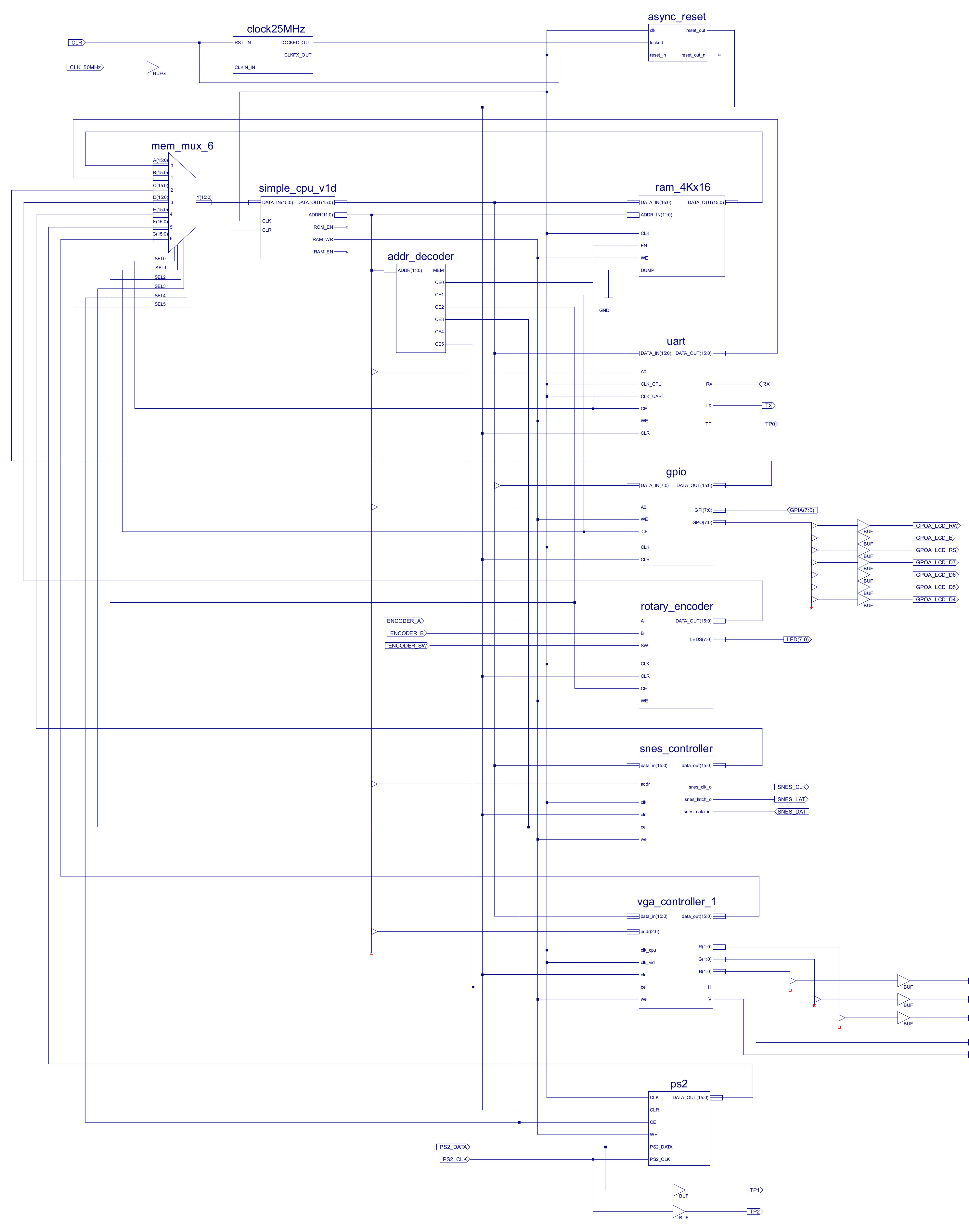
Figure 15: top level block diagram v1.1
A few hardware changes to this version, the obvious top-level change is a move from a 10MHz to a 25MHz processor clock, to give a little more processing power. Also some small hidden changes to the address map to make space for the new PS2 keyboard interface, the new memory map is shown below:
ADDR      A1 A0 CS       WR                        RD

0xFFF     1  1  0        UART_TX                   UART_RX
0xFFE     1  0  0        UART_TX                   UART_STATUS

0xFFD     0  1  1        GPIO A out                GPIO A out
0xFFC     0  0  1        GPIO A out                GPIO A in

0xFFB     0  1  2        ROTARY_RESET              ROTARY_DATA
0xFFA     1  0  2        SNES_DATA                 NU
0xFF9     0  1  3        SNES_START                SNES_STATUS
0xFF8     0  0  3        PS2_RESET                 PS2_DATA

0xFF7     1  1  6        NU                        NU
0xFF6     1  0  6        VGA TILE_Y_REG
0xFF5     0  1  6        VGA TILE_X_REG
0xFF4     0  0  6        VGA CPU_DST_ADDR_REG
0xFF3     1  1  6        VGA CPU_COLOUR_REG        VGA TILE_POS
0xFF2     1  0  6        VGA CPU_DATA_IN_REG       VGA CPU_DATA_OUT_REG
0xFF1     0  1  6        VGA CPU_SRC_ADDR_REG
0xFF0     0  0  6        VGA CPU_CTL_REG           VGA CPU_STATUS_REG

0xFEF     1  1  MEM      RAM                       RAM
...                      ...                       ...
0x000     0  0  MEM      RAM                       RAM
Some small changes to the processor's instruction-set, expanding upon the processor used in the practicals. The new and improved instruction-set is shown below:
###################
# INSTRUCTION-SET #
###################

# NOTE : THIS ASSEMBLER IS ONLY FOR USE WITH THE GAMES CONSOLE SIMPLECPU_V1D

# INSTR   IR15 IR14 IR13 IR12 IR11 IR10 IR09 IR08 IR07 IR06 IR05 IR04 IR03 IR02 IR01 IR00
# MOVE    0    0    0    0    RD   RD   X    X    K    K    K    K    K    K    K    K
# ADD     0    0    0    1    RD   RD   X    X    K    K    K    K    K    K    K    K
# SUB     0    0    1    0    RD   RD   X    X    K    K    K    K    K    K    K    K
# AND     0    0    1    1    RD   RD   X    X    K    K    K    K    K    K    K    K

# LOAD    0    1    0    0    A    A    A    A    A    A    A    A    A    A    A    A
# STORE   0    1    0    1    A    A    A    A    A    A    A    A    A    A    A    A
# ADDM    0    1    1    0    A    A    A    A    A    A    A    A    A    A    A    A
# SUBM    0    1    1    1    A    A    A    A    A    A    A    A    A    A    A    A

# JUMPU   1    0    0    0    A    A    A    A    A    A    A    A    A    A    A    A
# JUMPZ   1    0    0    1    A    A    A    A    A    A    A    A    A    A    A    A
# JUMPNZ  1    0    1    0    A    A    A    A    A    A    A    A    A    A    A    A
# JUMPC   1    0    1    1    A    A    A    A    A    A    A    A    A    A    A    A  -- JUMP IF NEG

# CALL    1    1    0    0    A    A    A    A    A    A    A    A    A    A    A    A

# OR      1    1    0    1    RD   RD   X    X    K    K    K    K    K    K    K    K  -- IMM
# LHI     1    1    1    0    RD   RD   X    X    K    K    K    K    K    K    K    K  -- IMM

# RET     1    1    1    1    X    X    X    X    X    X    X    X    0    0    0    0
# MOVE    1    1    1    1    RD   RD   RS   RS   X    X    X    X    0    0    0    1
# LOAD    1    1    1    1    RD   RD   RS   RS   X    X    X    X    0    0    1    0  -- REG INDIRECT
# STORE   1    1    1    1    RD   RD   RS   RS   X    X    X    X    0    0    1    1  -- REG INDIRECT

# ROL     1    1    1    1    RSD  RSD  X    X    X    X    X    X    0    1    0    0
# ROR     1    1    1    1    RSD  RSD  X    X    X    X    X    X    0    1    0    1

# ADD     1    1    1    1    RD   RD   RS   RS   X    X    X    X    0    1    1    0
# SUB     1    1    1    1    RD   RD   RS   RS   X    X    X    X    0    1    1    1
# AND     1    1    1    1    RD   RD   RS   RS   X    X    X    X    1    0    0    0
# OR      1    1    1    1    RD   RD   RS   RS   X    X    X    X    1    0    0    1
# XOR     1    1    1    1    RD   RD   RS   RS   X    X    X    X    1    0    1    0

# ASL     1    1    1    1    RSD  RSD  X    X    X    X    X    X    1    0    1    1
# ASR     1    1    1    1    RSD  RSD  X    X    X    X    X    X    1    1    0    0

# MUL     1    1    1    1    RD   RD   RS   RS   X    X    X    X    1    1    0    1  -- 8 BIT OPERANDS
# -       1    1    1    1    RD   RD   RS   RS   X    X    X    X    1    1    1    0
# -       1    1    1    1    RD   RD   RS   RS   X    X    X    X    1    1    1    1
Improvements made are:
The final upgrade was to the CALL / RET stack, this was increased from a depth of 4 to a depth of 8. When writing game code i did find it was quite common to have a nested subroutines to a depth of 5 or 6. Then if you consider debugging calls to the serial port i.e. to display variables on a terminal during testing, it was very easy to get to a call depth of 8. Therefore, i added a new LIFO buffer i.e. stack, with a depth of 8. However, being lazy wrote this in VHDL, also decided to try a distributed RAM based design, rather than a flip-flop / register based one, this allows the stack depth to be easily increased if needed later.
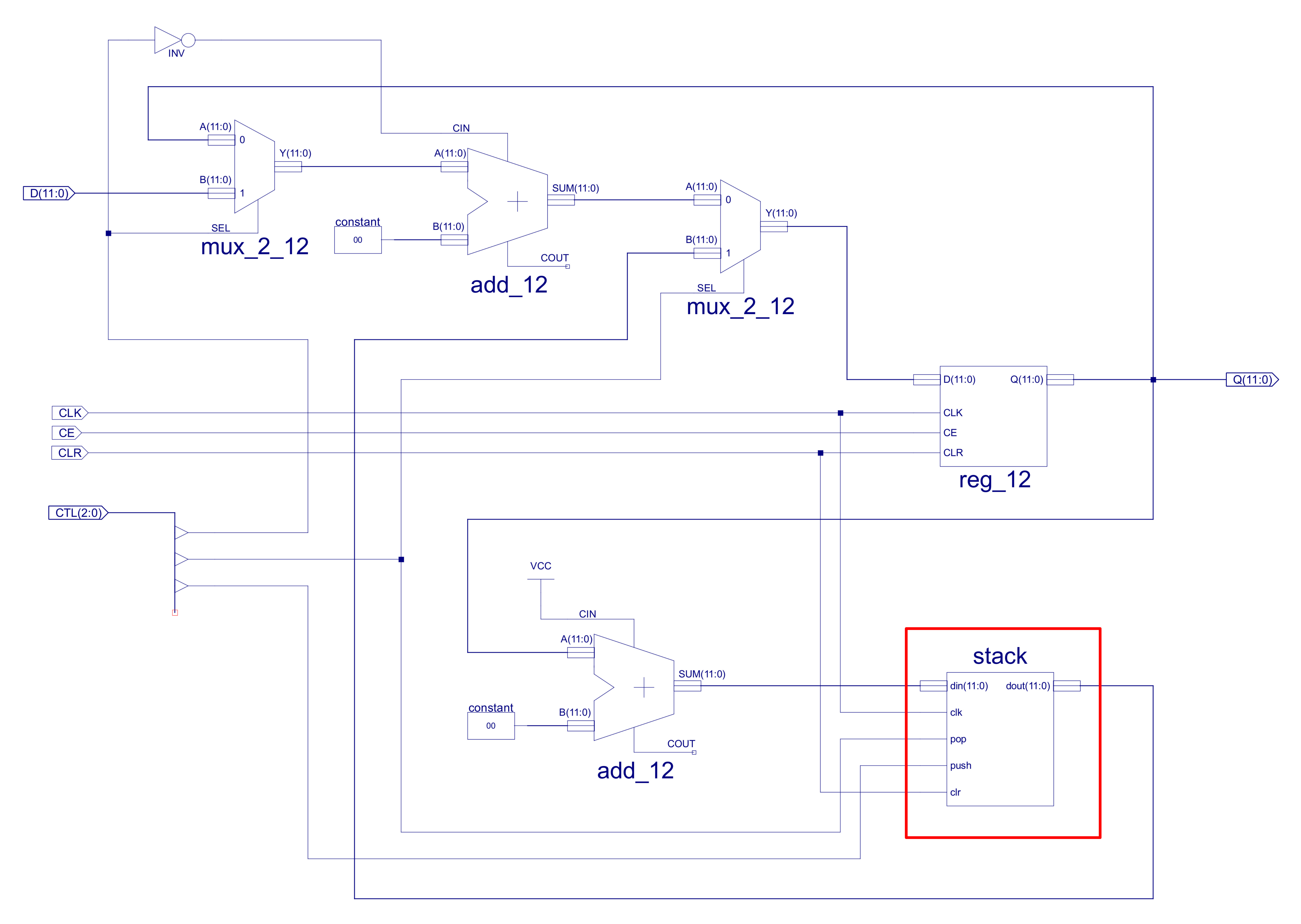
Figure 16: stack
library IEEE;
use IEEE.STD_LOGIC_1164.all;
use IEEE.STD_LOGIC_UNSIGNED.all;
use IEEE.Numeric_Std.all;

entity stack is
port(
  clk  : in  std_logic;
  clr  : in  std_logic;
  pop  : in  std_logic;
  push : in  std_logic;
  din  : in  std_logic_vector(11 downto 0);
  dout : out std_logic_vector(11 downto 0));
end stack;

architecture stack_arch of stack is

  signal count : std_logic_vector(2 downto 0);
  signal count_dec : std_logic_vector(2 downto 0);

  type ram_type is array (7 downto 0) of std_logic_vector(11 downto 0);
  signal RAM : ram_type;

begin

  counter : process( clk, clr )
  begin
    if clr = '1'
    then
      count <= (others=>'0');
    elsif clk'event and clk='1'
    then
      if push = '1'
      then
        count <= count + 1;
      elsif pop = '1'
      then
        count <= count - 1;
      end if;
    end if;
  end process;

  decrement : process( count )
  begin
    if clk'event and clk='1'
    then
      count_dec <= count - 1;
    end if;
  end process;

  ram_wr : process( clk )
  begin
    if clk'event and clk='1'
    then
      if push = '1'
      then
        RAM(to_integer(unsigned(count))) <= din;
      end if;
    end if;
  end process;

  dout <= RAM(to_integer(unsigned(count_dec)));

end stack_arch;
As with version 1, this version of the simpleCPU games console is again targeted for the Xilinx Spartan-3 FPGA board shown in figure 17. The FPGA configuration for this version is fixed to that shown in figure 15, but again the processor's memory i.e. the program running on this hardware, can be configured using the data2mem program, as described in the previous section above. This greatly reduces develop time as you do not need to re-synthesise the hardware, you can simply assemble your code and update an existing .bit file with a new memory configuration and then upload into the FPGA. To allow you to do this you will need the following files:
Note, do read the documentation for version 1.0, as workflow is the same, but then to write your own games, download the software tools using the above link, edit the go.sh / go.bat file to select your game code, run this script, then run the update_computer_bit_file.sh / update_computer_bit_file.bat script to generate a new_computer.bit configuration file and then use Impact to upload this onto the FPGA. Finally, play game :).
ToDo: works in Linux, but i need to double check the above scripts in Windows, i think there will be some small fixes needed in these scripts, as described in the previous section.

Figure 17: FPGA board
To understand how to program this version of the games controller i have created a series of video tutorials. These talk through how to use the VGA controller (Link) and the other peripheral devices (Link). Note, some small changes between version 1.0 and 1.1, but basically the same.
This video introduces the background to the games console and hardware used to implement it.

Figure 18: SimpleCPU Games Console : An Overview (Link)
The first peripheral device considered is the video display controller (VDC). In this video the following example code is discussed:

Figure 19: SimpleCPU Games Console : VDC frame buffer read / write (Link)
To simplify the drawing of "blocky" graphics the VDC support block write and block copy functions, simplifying the process of writing data to the frame buffer. In this video the following example code is discussed:

Figure 20: SimpleCPU Games Console : VDC block write / copy (Link)
To show how the Block write and copy commands can be used to implement a simple game, we consider a bouncing ball "game". In this video the following example code is discussed:

Figure 21: SimpleCPU Games Console : Game 1 (Link)
The core graphical construct used in the VDC is the tile, a library of 128, 8x8 graphical elements defined in video memory. In this video the following example code is discussed:

Figure 22: SimpleCPU Games Console : VDC tile draw / overlay (Link)
Still need to record videos for the following topics
SimpleCPU Games Console : VDC "sprites", well tiles + sprite like functionality :) (Link)
SimpleCPU Games Console : Serial port and LCD display (Link)
SimpleCPU Games Console : Rotary encoder, SNES games pad and PS2 keyboard (Link)
Below are some video demos of some games that have been written so far.
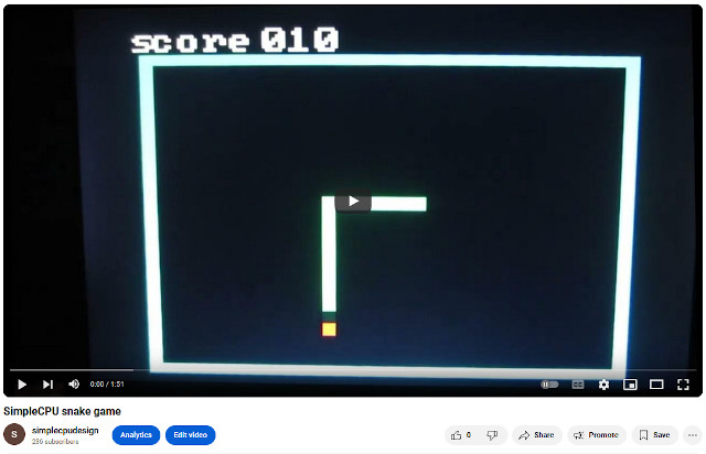
Figure 23: Snake (Link)
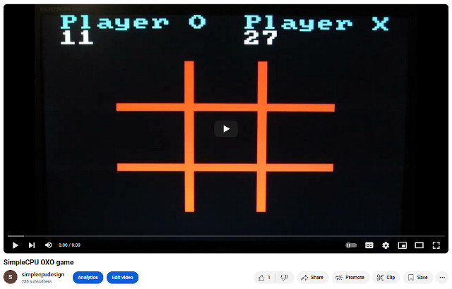
Figure 24: OXO (Link)
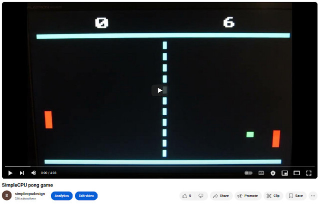
Figure 25: Pong (Link)
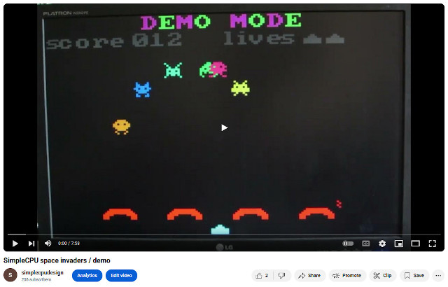
Figure 26: Space invaders (Link)
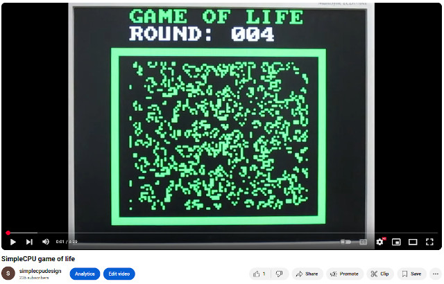
Figure 27: Game of life (Link)
To help develop games especially an AI opponent for the OXO game an instruction set simulator has been developed. You can download this simulator and an OXO test program here:
WORK IN PROGRESS

This work is licensed under a Creative Commons Attribution-NonCommercial-NoDerivatives 4.0 International License.
Contact email: mike@simplecpudesign.com