After playing around with the simpleCPU versions 1a, 1b and 1c, i decided to pause and take stock, to consider what type of architecture and features an introductory teaching processor should have. Therefore, i decided to construct a simulation model of the simpleCPU_v1a processor and its memory. Using this simulation model different hardware architectures and instruction sets can be tested without the need to build any hardware, breaking each instruction down into a series a micro-instructions (internal steps) that define the processor's Fetch - Decode - Execute (FDE) cycle. The simulation package i decided to use is CPUSim Link:
CPUSim simulates computer architectures at the register-transfer-level (RTL). That is, the basic hardware units from which a hypothetical CPU is constructed e.g. registers, condition bits, memory (RAM) etc. The user does not need to deal with individual transistors or gates on the digital logic level of a machine. The basic units used to define machine instructions consist of microinstructions of a variety of types. The details of how the micro-instructions get executed by the hardware are not important at this level. - CPUSim User Manual
In addition to simulating the processor's hardware CPUSim also allows the user to define the processor's instructions i.e. mnemonics, and evaluate each instruction's structure, the bit-fields used for opcode and operand etc. These instruction definitions are used in CPUSim to create a customer assembler, allowing the processor's hardware and software to be evaluated by single stepping through a program at a machine-instruction level, or at the micro-instruction level.
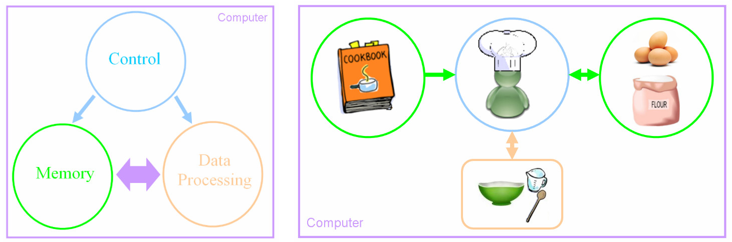
To understand what is happening within a computer we first need to understand what are the basic building blocks of any computer, these are: Control, Memory and Data processing, as shown in figure 1. Note, control is highlighted blue, memory green and data processing orange.
Figure 1: the building blocks of any computer
The analogy i like to use to explain how a computer executes a program is a chef baking a cake. The chef reads (fetches) an instruction from the recipe book. They then pause to understand (decode) that instruction, selects the cooking implements need to perform the task e.g. bowls, spoons etc, and gets the ingredients from the cupboard that they will need. Once they have everything need, they then perform (execute) that step of the recipe. These steps are then repeated until the recipe (program) has been completed, as shown in figure 2.
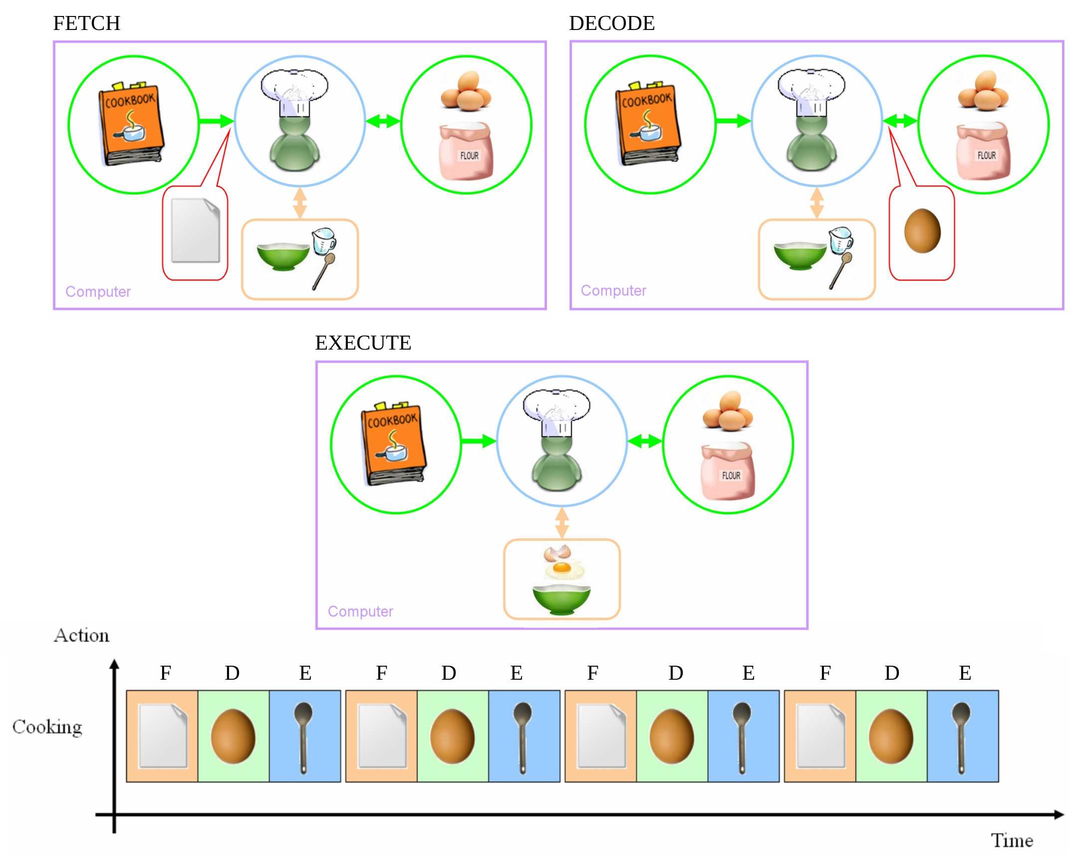
Figure 2: Fetch - Decode - Execute cycle.
Some key points to pull out of this description:
Now that we have a basic understanding of what is going on, we can start to build our simulator.
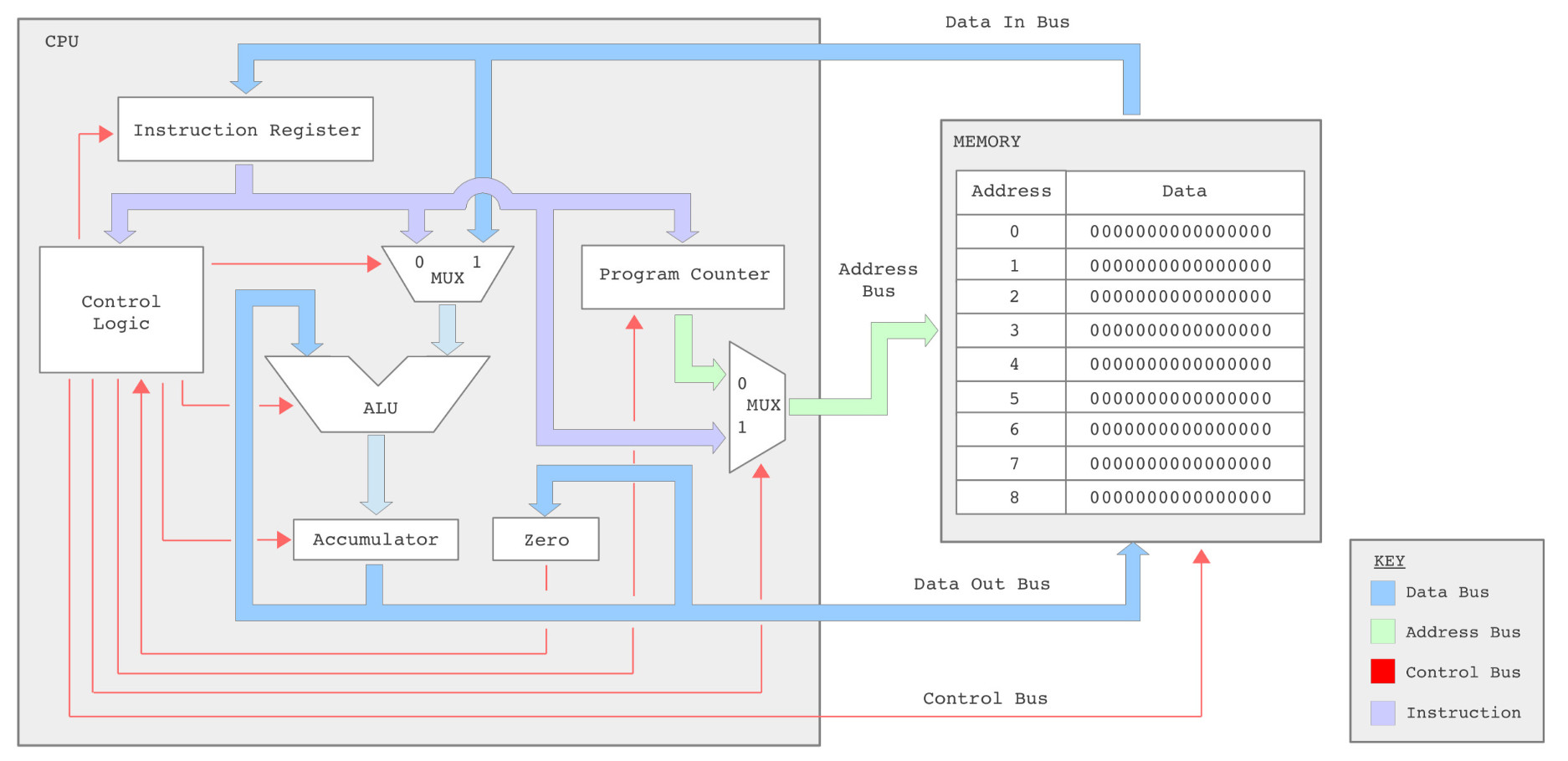
Figure 1: simpleCPUv1a block diagram
To construct the simulation model of the simpleCPU the RTL modules are first defined. Describing a CPU's functionality at this level removes a lot the implementation detail e.g. multiplexers, ALU etc, shown in figure 1, simplifying the CPU's operations to the movement of data between registers (memory elements). The RTL block diagram for this computer is shown in figure 2. Note, the ALU's functionality (+,-,*,/) and switching multiplexers (MUX) are implicit in the description and therefore no longer shown.
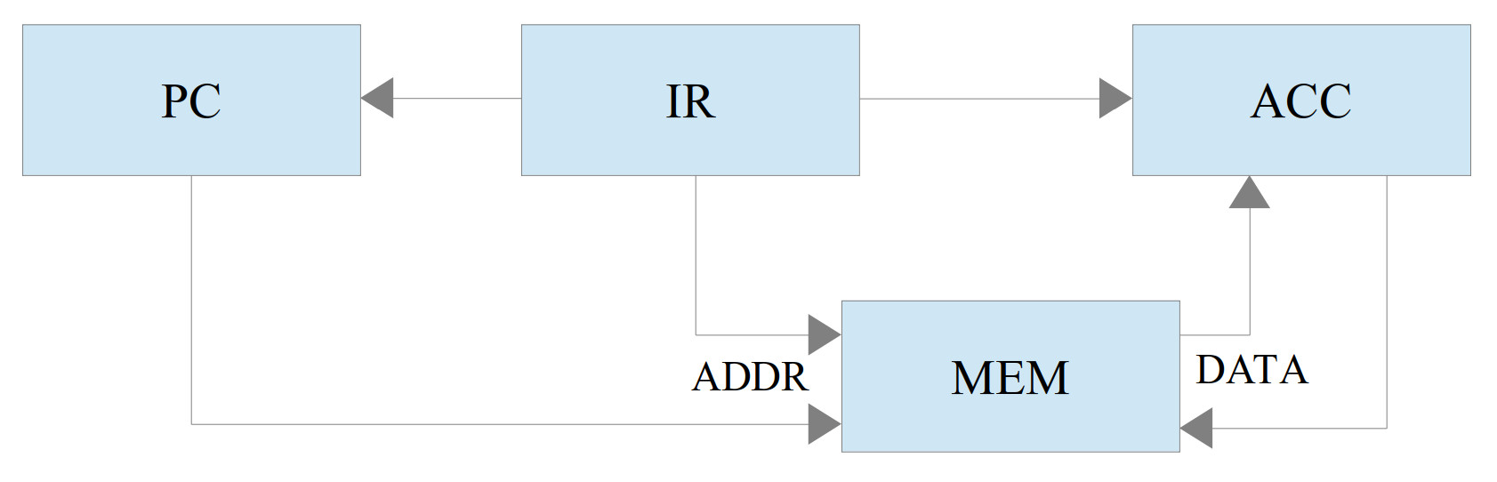
Figure 2: Register Transfer Level (RTL) block diagram
The processor has three main registers:
The interconnection and the flow of data between these registers is indicated by the connecting arrows show in figure 2. Memory elements that are not connected cannot transfer data e.g. there is no path from the PC to the ACC, therefore, the PC value can not be transferred to the ACC or vice-versa. This can be confirmed if you examine the data paths in the block diagram shown in figure 1.
Note, the following points below are a little bit of an aside, but I thought it would be useful to explain why this processor's architecture differs from the ones you will find in standard textbooks and CPUSim's example processor: Wombat. These processors have the following additional registers :
To keep the SimpleCPU simple (reduce hardware) these are not included in this design. This raises the question why are they included in the other architectures. The main reasons are mainly linked to :
All of these features come at the cost of increased hardware costs, therefore, as the simpleCPU will be implemented within an FPGA, and as processing speed isn't a high priority i.e. there are no tight timing closure issues, the MDR and MAR registers are not required. This allows use to follow the wise words of Keep It Simple Stupid (KISS).
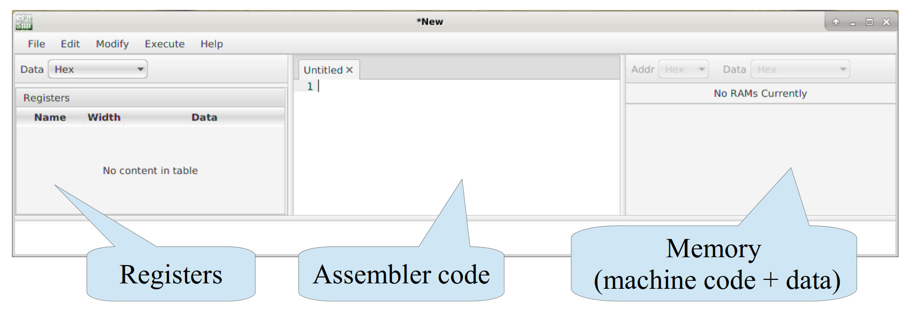
Figure 3: CPUSim main window
The initial CPUSim stating screen is shown in figure 3, displaying internal registers, assembly code and external memory. The first step in creating the simulator is to define the processor's registers and memory. To add the registers shown in figure 2 to the simulation model left click on the pull down menu:
Modify -> Hardware modules ...
This will open the ‘Edit modules’ window, left click on the pull down menu:
Type of Module -> Register
Left click the 'New' button at the bottom of this window. This will add a new row to the register table using the default name '?'. You can then double left click in these text boxes and enter each register's name and data width as shown in figure 4. Note, the addr, data and status registers were added to overcome limitations in the simulator, they do not exist in the actual hardware (discussed in more detail later).
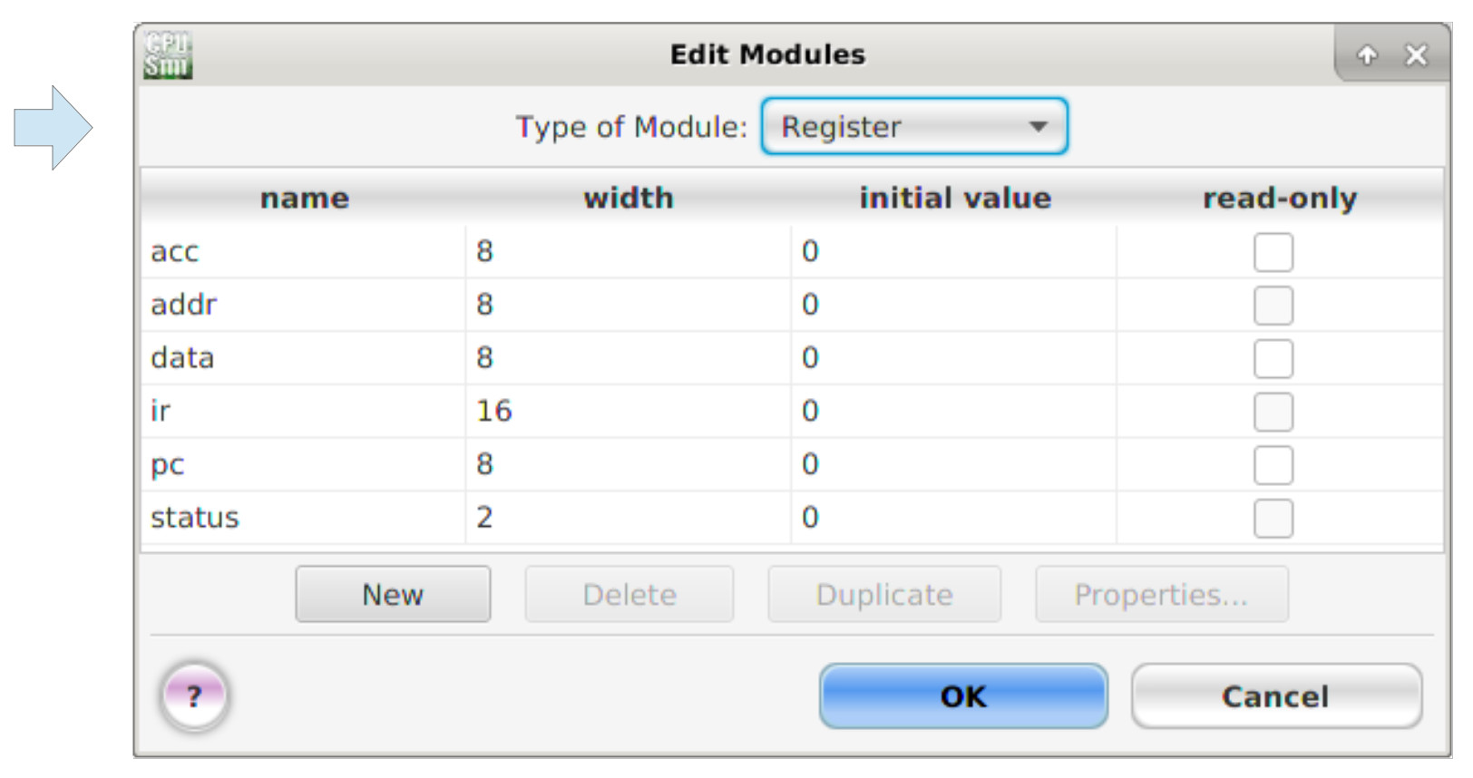
Figure 4: processor registers
To add condition bits (flags) single left click on the pull down menu:
Type of Module -> ConditionBit
Left click the 'New' button and enter the condition bit names and bit positions as shown in figure 5. A condition bit must be assigned to a register, therefore, click within the register text box to display a pull down menu of the previously defined registers, select 'status'. In addition to the normal ALU flags a 'halt' flag has also been included. When set, this flag signals to the simulator that the execution of the current assembly language program should be stopped.
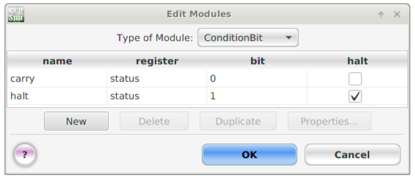
Figure 5: CPU condition bits
Note, the processor does contain a zero flag (Z), which is set when the ACC contains a zero value. However, in CPUSim this flag is defined differently, as described later. The final hardware module to be defined is the computer's memory, single left click on the pull down menu:
Type of Module -> RAM
Left click the 'New' button and enter the memory name and size as shown in figure 6. Left click on the OK button to finish.
Figure 6 : computer's memory
Note, the simpleCPU processor is based on a Von Neumann architecture (Link), i.e. a stored program computer, using one memory that contains both instructions and data.
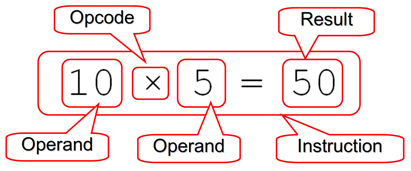
Figure 7 : whats in an instruction?
An instruction defines the data to be processed (operands), the function to be performed (opcode) and where the result (if any) will be stored. This processor uses a fixed length, 16 bit instruction format i.e. all instructions are the same size. Each instruction within the CPU's instruction-set is implemented by a set of micro-instructions i.e. the set of Register Transfer Level (RTL) operations that must be performed to implement the desired functionality. Micro-instructions also define the step-by-step sequence of operations needed to perform the fetch-decode-execute cycle.
Note, micro-instructions are internal to the processor, completely separate from the processor's instruction-set i.e. machine-level instructions. Micro-instructions are not directly accessible to a programmer.
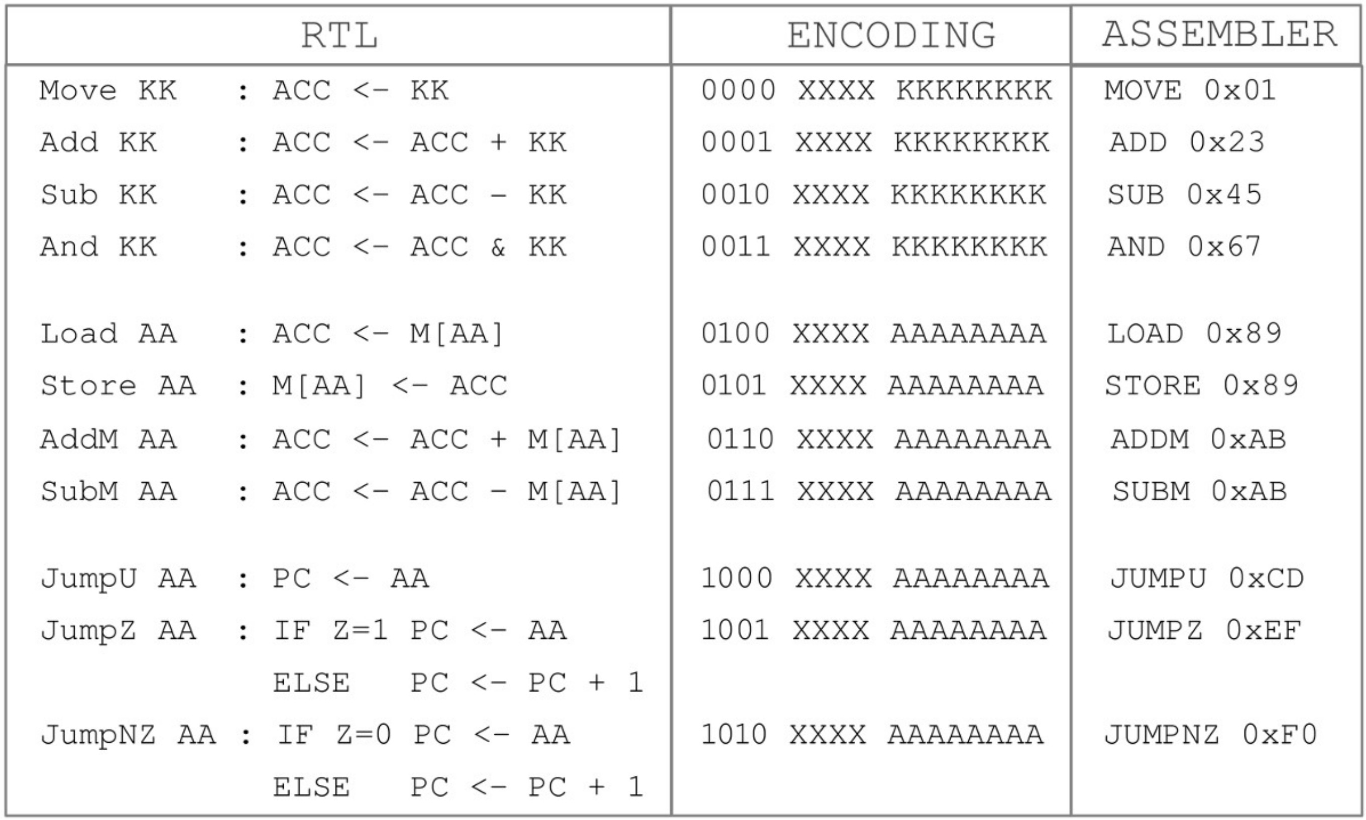
Figure 8 : instruction set
The complete set of instructions supported by the simpleCPU_v1a are listed in figure 8, along with their RTL descriptions, bit-fields and examples of their typical usage. Note, XX=Not Used, KK=Constant, AA=Address. Two fundamental machine-level instructions for any processor are the MOVE and ADD instructions, as shown below:
start:
	move 0x01		;move the value 1 into ACC.
	add  0x02		;add the value 2 to the ACC
This processor has an accumulator based architecture i.e. it has one general purpose data register (ACC), therefore, its instruction set uses a 1-operand instruction format. This means that instructions do not need to define the second operand, or where the result will be stored, as it is always the ACC. Note, computer architectures are sometimes defined by the number of operands used:
An instruction's operands define where data is stored and results saved. Therefore, the size of an instruction i.e. the number of bits needed to represent it, is dependent on the number of operands processed, the number of opcodes (instructions) and the number of addressing modes supported by a processor. Note, a key point to appreciate is that the size of an instruction is largely independent of the types of data it processes. This can cause problems in how instructions and data are stored in memory e.g. the SimpleCPU uses 8 bit data and 16 bit instruction widths. How this size difference is handled is discussed later.
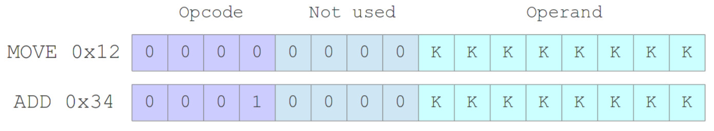
Figure 9 : MOVE and ADD instruction formats
The bit-fields used to define the MOVE and ADD instructions are shown in figure 9. These instructions use the immediate addressing mode i.e. the operand they process is an 8 bit constant (K bits) that is 'immediately' available form the instruction register (IR) after the instruction fetch. To add these new machine-instructions to the simulation model single left click on the pull down menu:
Modify -> Machine Instructions
This will open the 'Edit machine instructions' window, as shown in figure 10. Before we can create a new instruction we must define the bit-fields used e.g. opcode, not-used and operand, as highlighted in figure 9. To define these bit-fields left click on the 'Edit fields' button. Next, left click the 'New' button at the bottom of this window. This will add a new row to the fields table using the default name '?'. Double left click in these text boxes and enter each field names, type and widths as shown in figure 11.
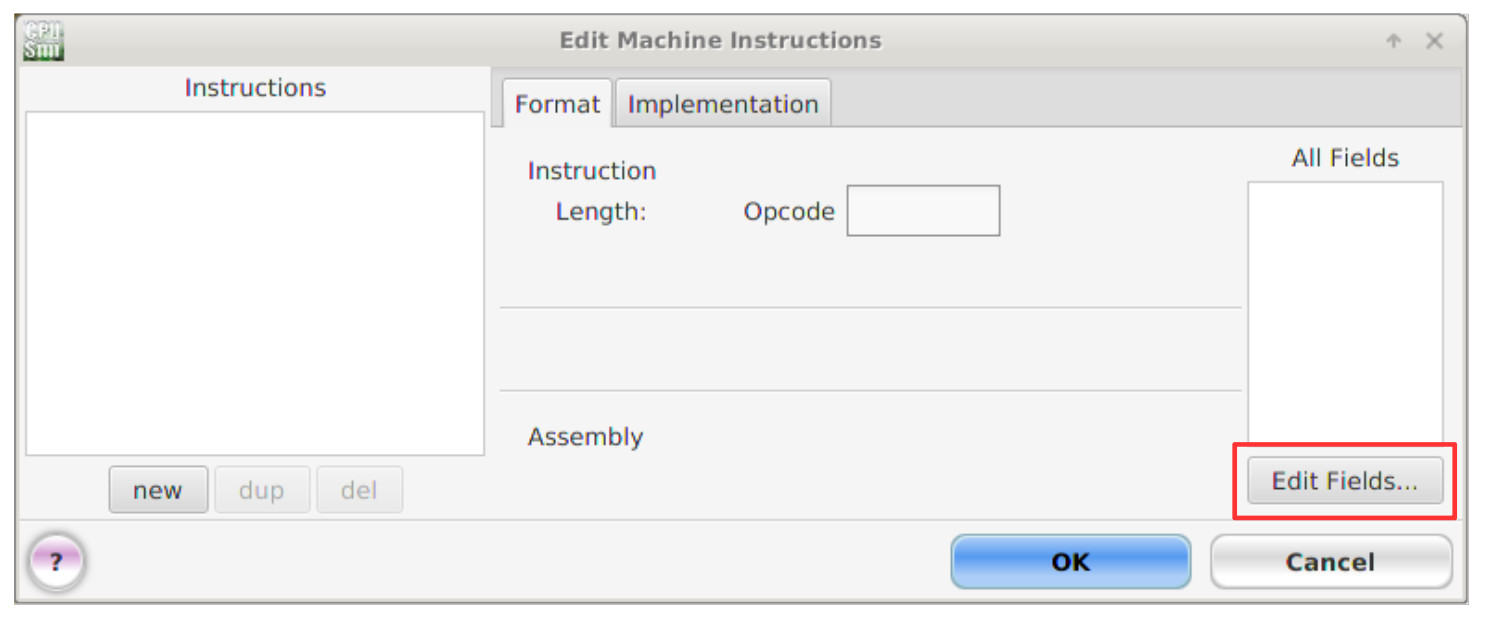
Figure 10 : Edit machine-instructions window
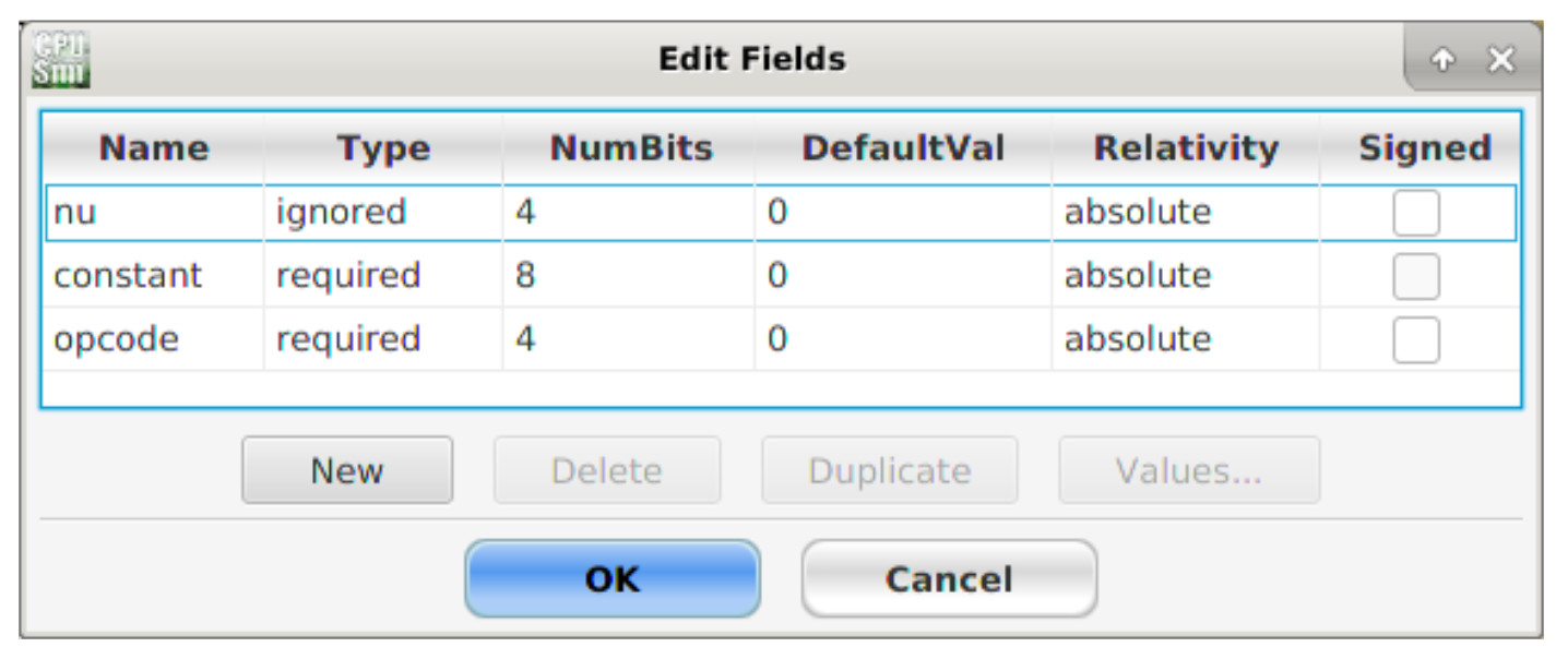
Figure 11 : Edit bit-fields window
Within the 'Edit machine instructions' window left click on the 'New' button at the bottom left of this window. This will add a new row to the instructions list using the default name '?'. Double left click in these text boxes and enter the name move. Next, left click hold and drag the required bit-fields from the 'All fields' list into the middle instruction panel. The instruction formats for the MOVE and ADD instructions are shown in figure 12. Note, the Assembly panel (bottom) will update automatically.
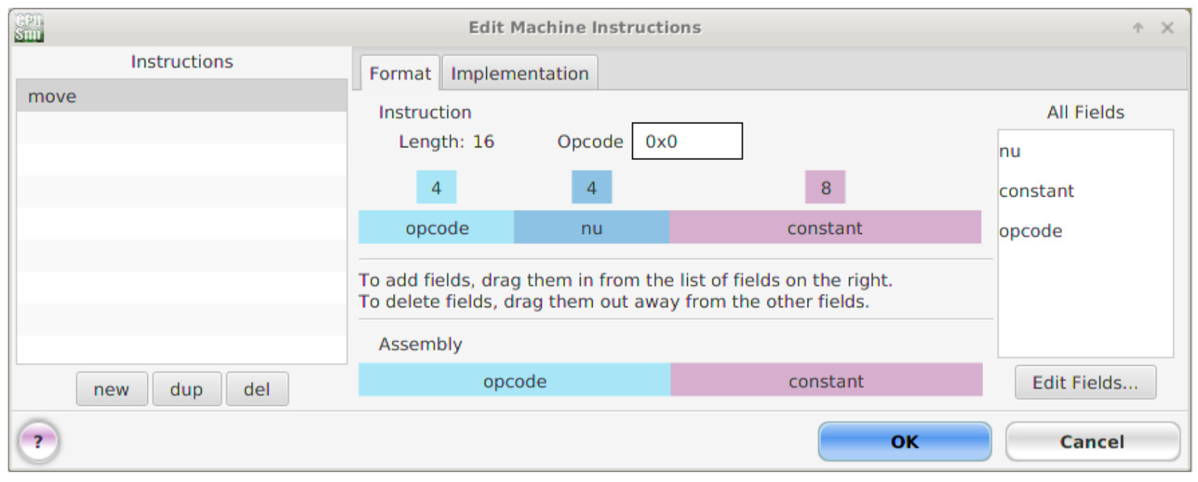
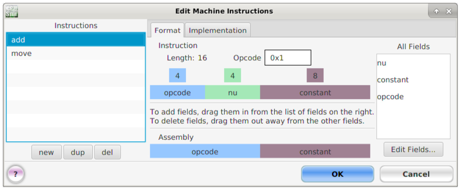
Figure 12 : MOVE and ADD instructions
Note, the opcode values for MOVE (0) and ADD (1) can be different values, the key requirement is that they are unique i.e. no two machine-level instructions can have the same opcode.
To define what these instructions should do within the simulator we need to define the step-by-step sequence of operations they perform i.e. their micro-instructions. To add a new micro-instruction to the simulation model left click on the pull down menu:
Modify -> Microinstructions ...
This will open the ‘Edit Microinstructions’ window, single left click on the pull down menu:
Type of Microinstruction -> TransferRtoR
This first group of micro-instructions are those involved in transferring data between registers. To implement the MOVE instruction we need to move the constant KK from the instruction register (IR) to the accumulator (ACC). To implement these micro-instructions left click the 'New' button. This will add a new row to the micro-instruction table using the default name '?'. Double left click in this text box and enter the micro-instruction names and parameters as shown in figure 13.
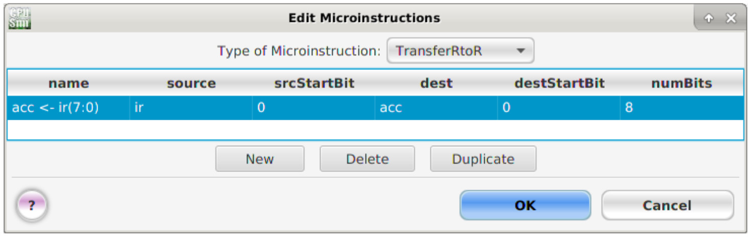
Figure 13 : TransferRtoR micro-instructions
TransferRtoR micro-instruction fields:
To implement the ADD instruction we need to add the constant K from the instruction register (IR) to the accumulator (ACC). To do this left click on the pull down menu:
Type of Microinstruction -> Arithmetic
Next, enter the micro-instruction names and parameters as shown in figure 14.
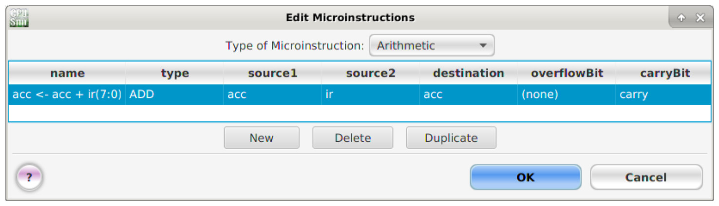
Figure 14 : TransferRtoR micro-instructions
Arithmetic micro-instruction fields:
The MOVE and ADD machine-instruction are very simple and can be executed using the two micro-instructions defined. However, to allow the processor to load these instruction from memory and process them we need to also define the micro-instructions needed in the Fetch and Decode phases. To read data/instructions memory left click on the pull down menu:
Type of Microinstruction -> MemoryAccess
Next, enter the micro-instruction names and parameters as shown in figure 15.
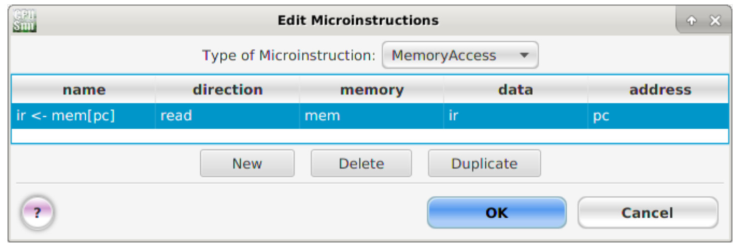
Figure 15 : MemoryAccess micro-instructions
MemoryAccess micro-instruction fields:
After the completion of the instruction fetch the program counter (PC) is incremented to the next instruction address. In the event the program counter overflows i.e. changes from 0xFF to 0x00 (max address is 255), the halt flag is set, signalling to the simulator that an error has occurred i.e. the program has run out of memory. To define the increment micro-instruction, left click on the pull down menu:
Type of Microinstruction -> Increment
Next, enter the micro-instruction name and parameters as shown in figure 16.
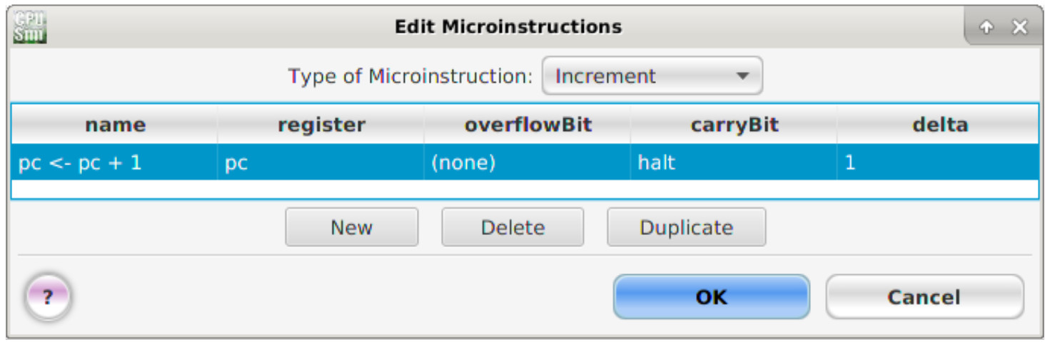
Figure 16 : Increment micro-instruction
The final micro-instruction simply defines what internal register holds the current instruction to be executed i.e. the instruction register (IR), left click on the pull down menu:
Type of Microinstruction -> Decode
Next, enter the micro-instruction name and parameters as shown in figure 17.
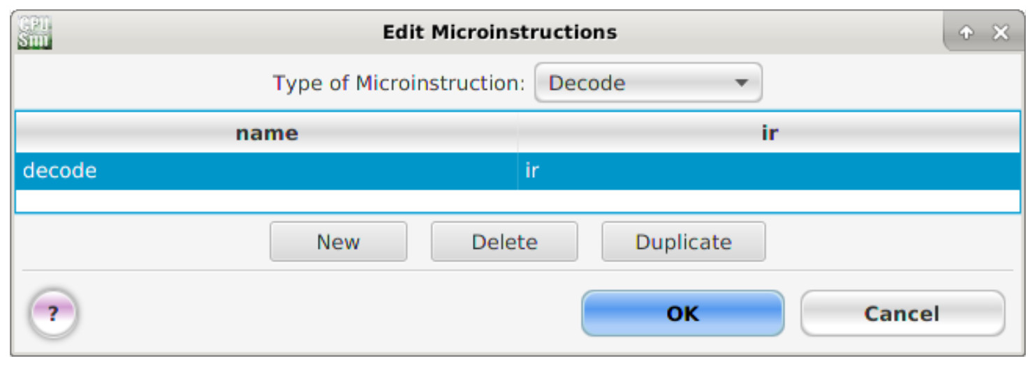
Figure 17 : Decode micro-instruction
Using these micro-instructions we can now define the processor's Fetch - Decode - Execute (FDE) cycle at the register transfer level (RTL). To add these operations to the simulation model left click on the pull down menu:
Modify -> Fetch sequence ...
This will open the 'Edit Fetch Sequence' window, expand the micro-instruction category folders by clicking on the triangle icon. Then left click, hold and drag the required micro-instruction into the 'Fetch Sequence Implementation' panel, as shown in figure 18. The first micro-instruction fetches the next instruction pointed to by the PC, saving it into the IR. The PC is then incremented, finally the instruction in the IR is decoded.
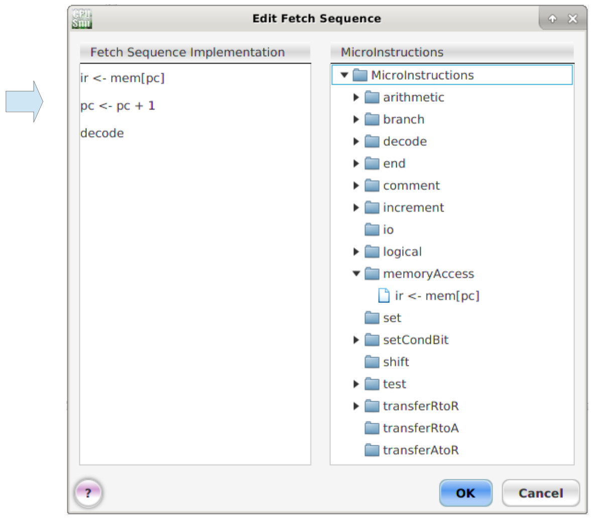
Figure 18 : Fetch-Decode sequence
Note, if you insert the wrong micro-instruction, left click, hold and drag that micro-instruction out of the sequence panel back into the micro-instruction panel. If needed you can also changing the order that the fetch sequence is performed by again left clicking, hold and dragging the micro-instruction up or down the sequence list. Within CPUSim the micro-instructions defined in the Fetch-Decode sequence are performed sequentially, finishing when the decode micro-instruction is performed. In the hardware one or more micro-instructions could be performed in parallel to improve processing performance.
To define the micro-instructions used by each machine-instruction left click on the pull down menu:
Modify -> Machine Instructions
This will open the 'Edit machine instructions' window, left click on the 'Implementation' tab. Next, expand the micro-instruction category folders by clicking on the triangle icon. Then left click, hold and drag the required micro-instruction into the 'Execute Sequence' panel, as shown in figure 19. Note, micro-instruction can be moved or removed as previously described. All machine-instruction sequences must finish with the predefined end micro-instruction to terminate the FDE cycle.
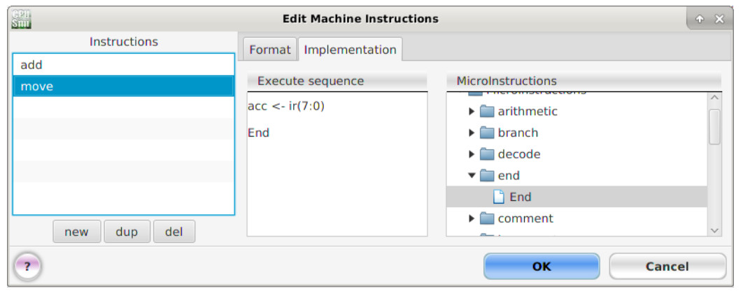
Figure 19 : Adding MOVE and ADD micro-instructions
Note, each micro-instruction name describes the function to be performed using the standard register transfer language syntax :

Figure 20 : micro-instruction syntax
A high level program is broken down into a series of machine-instructions, these in turn are performed using the Fetch-Decode-Execute cycle, which in turn are implemented inside the computer as a series of micro-instructions. As this version of the simpleCPU has a hardwired controller i.e. a controller that produces control signals directly from the decoded opcode field, multi-step execution phases are not really possible i.e. each machine-level instruction is relatively simple. To enable more complex machine-level instructions we would need to goto a micro-programmed controller as used in the simpleCPU_v2 (Link)
The full set of immediate addressing mode instructions supported by the SimpleCPU processor are shown in figure 21, to help machine-code "readability" the top two bits of the opcode field for an instruction using this address mode are always "00".
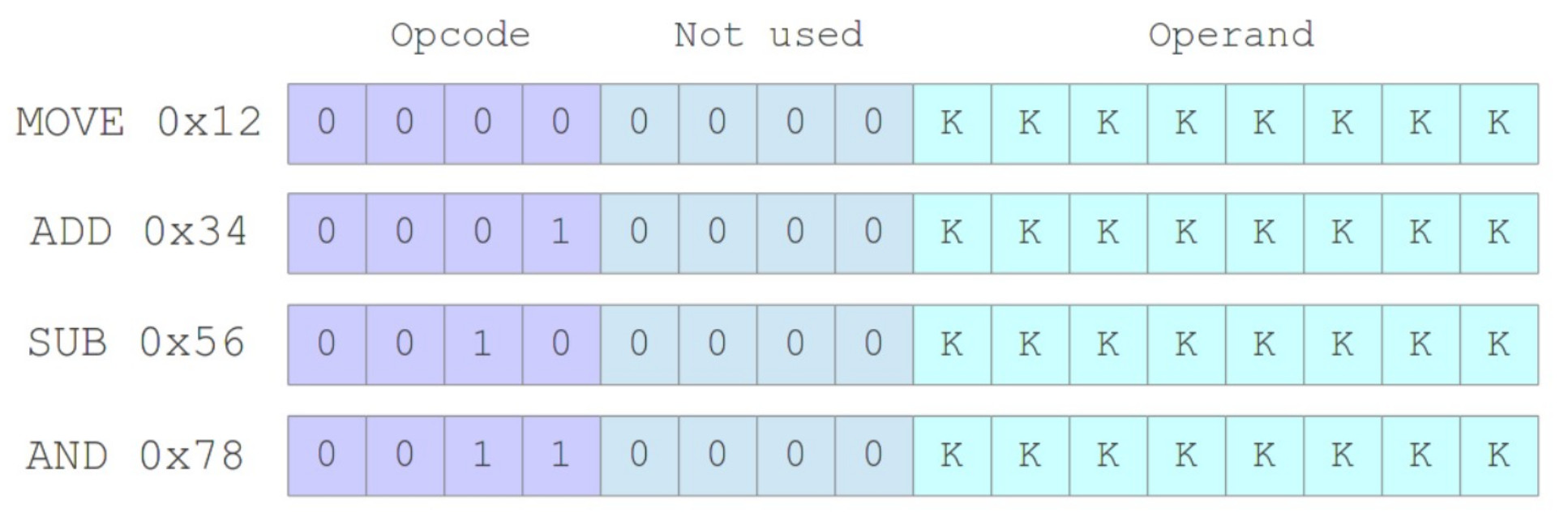
Figure 21 : Immediate addressing mode instructions
The SUB instruction can be implemented using the same process as the ADD instruction. A small complication, in CPUSim you can only perform logical micro-instructions upon registers of the same size. Therefore, to implement the AND instruction we will need to implement another register-to-register transfer instruction to load the lower 8 bits of the instruction register into the data "register", this can then be used as an operand source for the bitwise AND micro-instruction. In the actual hardware this "register" is simply implemented using wires, selecting bits IR(7:0), as no memory functionality is required i.e. its a simple bit-slice operation. The micro-instructions for the AND instruction are shown in figure 22.
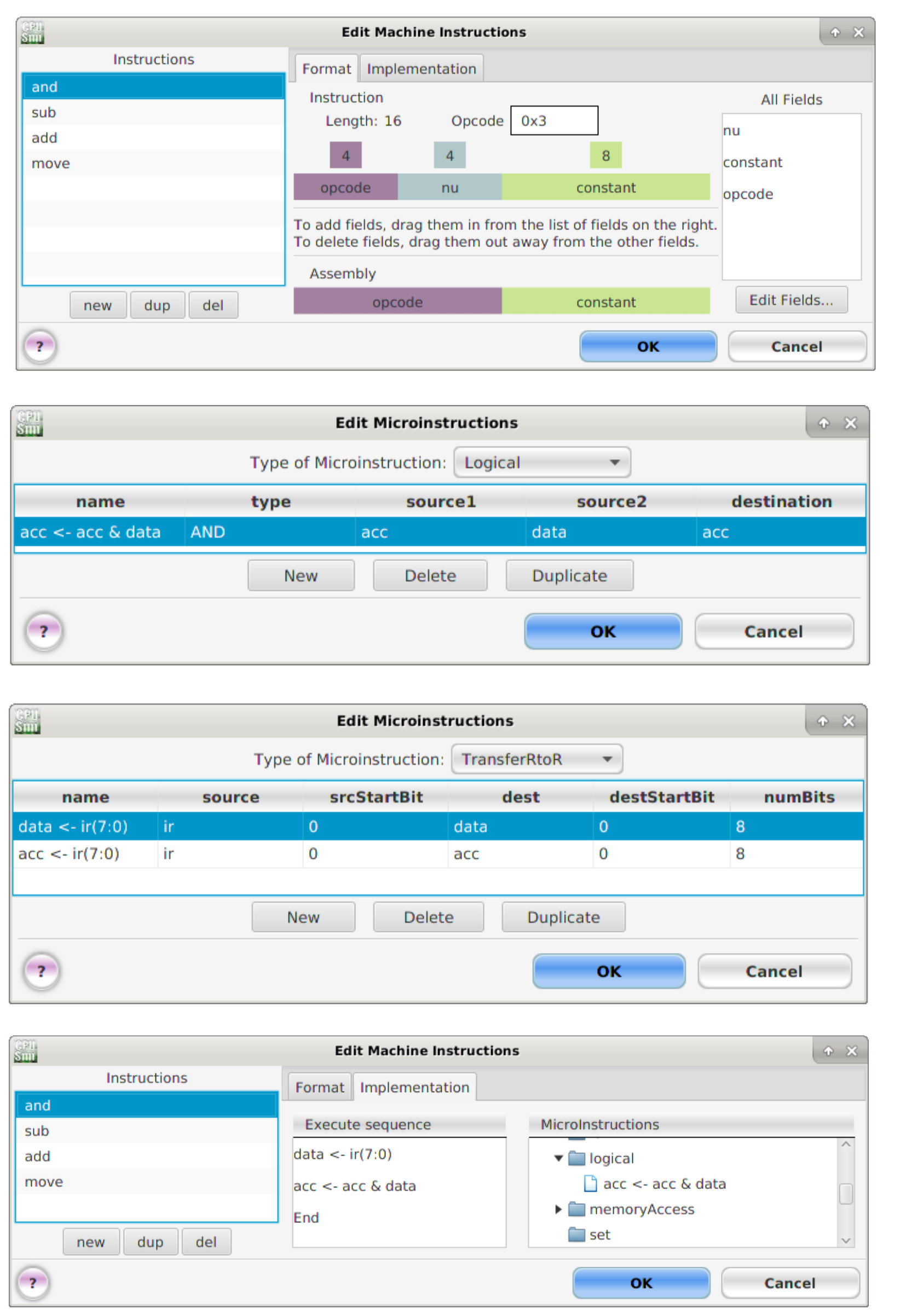
Figure 22 : AND instruction machine/micro instructions
A key requirement of any computer is the ability to process variables stored in memory. Therefore, the processor needs to support the absolute, or direct addressing mode i.e. LOAD and STORE instructions. To introduce these ideas consider the simple program shown below.
start:
	load  0x03	;read data at address 0x03 into ACC
	add   0x01	;increment data in ACC
	store 0x03	;write ACC to address 0x03
This program loads the data stored at address 3 into the ACC, increments its values, before writing it back to memory. The bit-fields used to define the LOAD and STORE instructions are shown in figure 23. These instructions use the absolute addressing mode i.e. the operand they process is an 8 bit address (A bits), used to access data from memory stored at the specified "absolute address". Note, this address is stored in the instruction register (IR) after the instruction fetch phase.
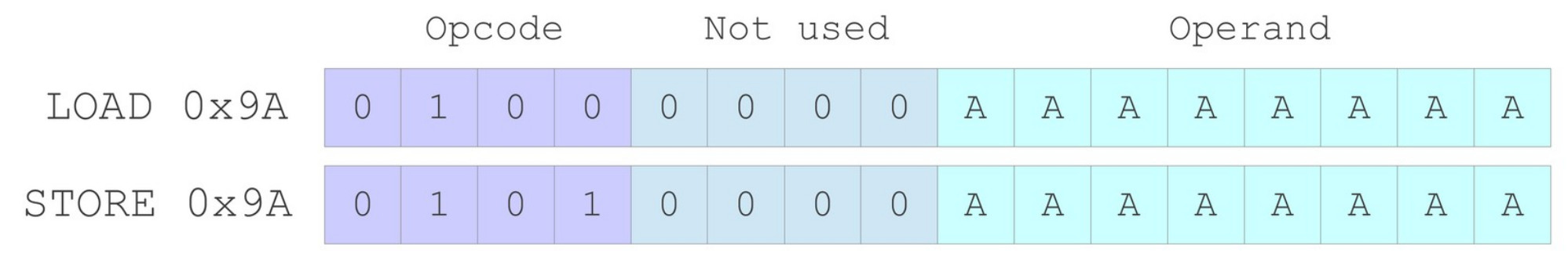
Figure 23 : LOAD and STORE instructions.
LOAD and STORE instructions are data movement instructions. These types of instructions are just as important from a data processing point of view as the number crunching instructions (+,-,x,/). When you start to look at what happens in a computer its surprising how much time is spent just moving data, therefore, efficient data transfers are the key to good processing performance.
Another, small complication, is that in CPUsim you can only perform memory access micro-instructions using registers. Therefore, we will need to implement another register-to-register transfer micro-instruction to load the lower 8 bits of the instruction register (IR) into the addr "register", this can then be used as the address within the micro-instruction. In the actual hardware this "register" is simply implemented using wires, selecting IR(7:0), as no memory functionality is required i.e. its a simple bit-slice operation. The machine and micro instruction need to implement these instructions is shown in figures 23 ans 24.
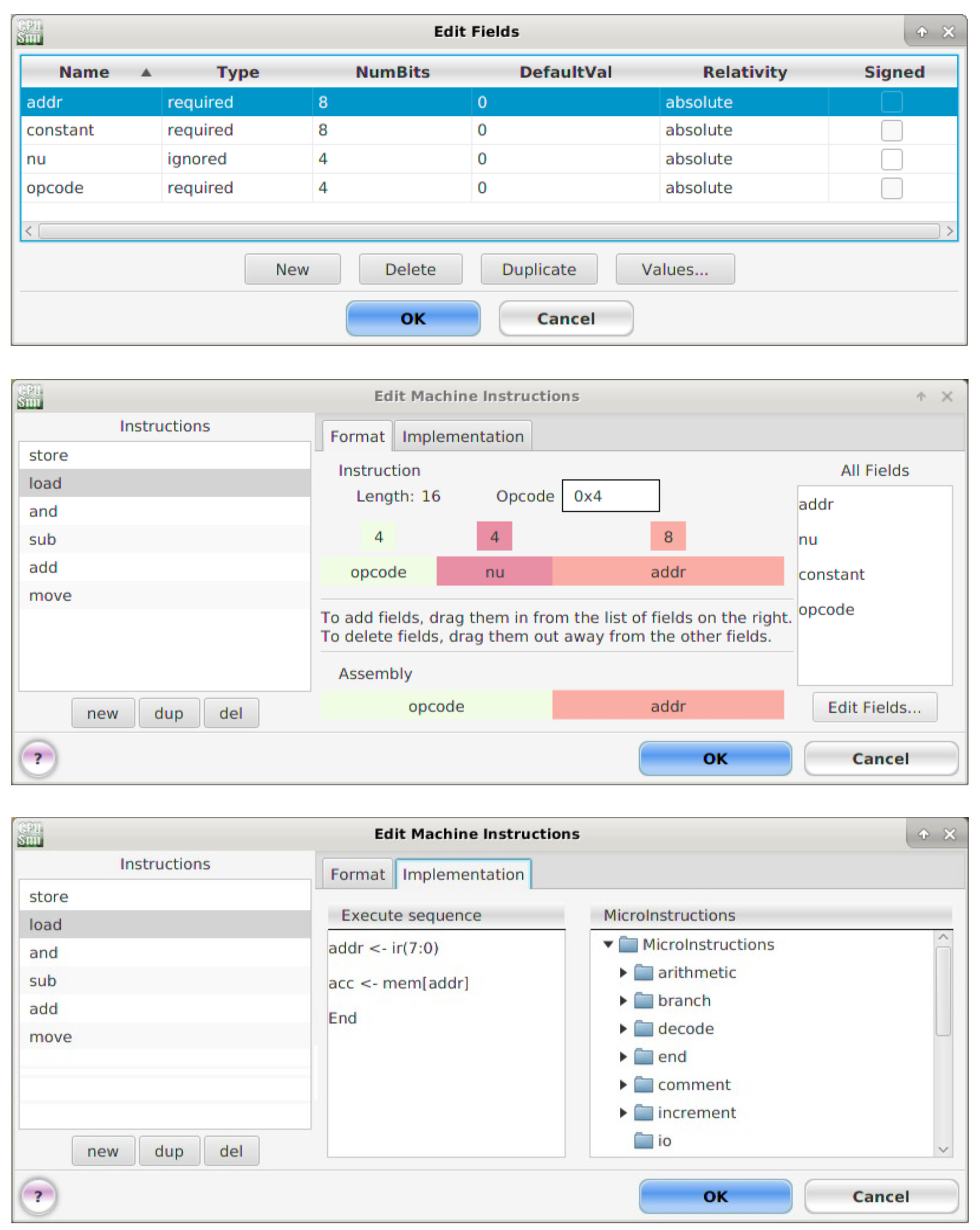
Figure 23 : LOAD machine and micro instructions.
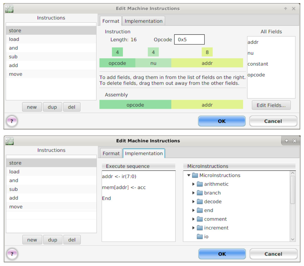
Figure 24 : STORE machine and micro instructions.
The full set of absolute addressing mode instructions supported by the SimpleCPU processor are shown in figure 25. Note, to help machine-code "readability" the top two bits of the opcode field for an instruction using this address mode are always "01".
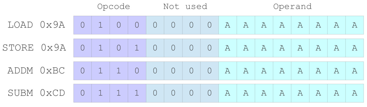
Figure 25 : Absolute addressing mode instructions.
Another small complication when implementing the ADDM and SUBM instructions in the simulator is that you can only perform arithmetic micro-instructions using registers. Therefore, we will need to implement a new MemoryAccess micro-instruction to transfer the value accessed from memory into the data "register", this can then be used as the second operand in the new arithmetic micro-instructions. In the actual hardware this "register" is simply implemented using wires, selecting the data-out bus from memory: MEM(7:0), as no memory functionality is required i.e. again its a simple bit-slice operation. The ADDM and SUBM machine and micro instructions are shown in figures 26 and 27.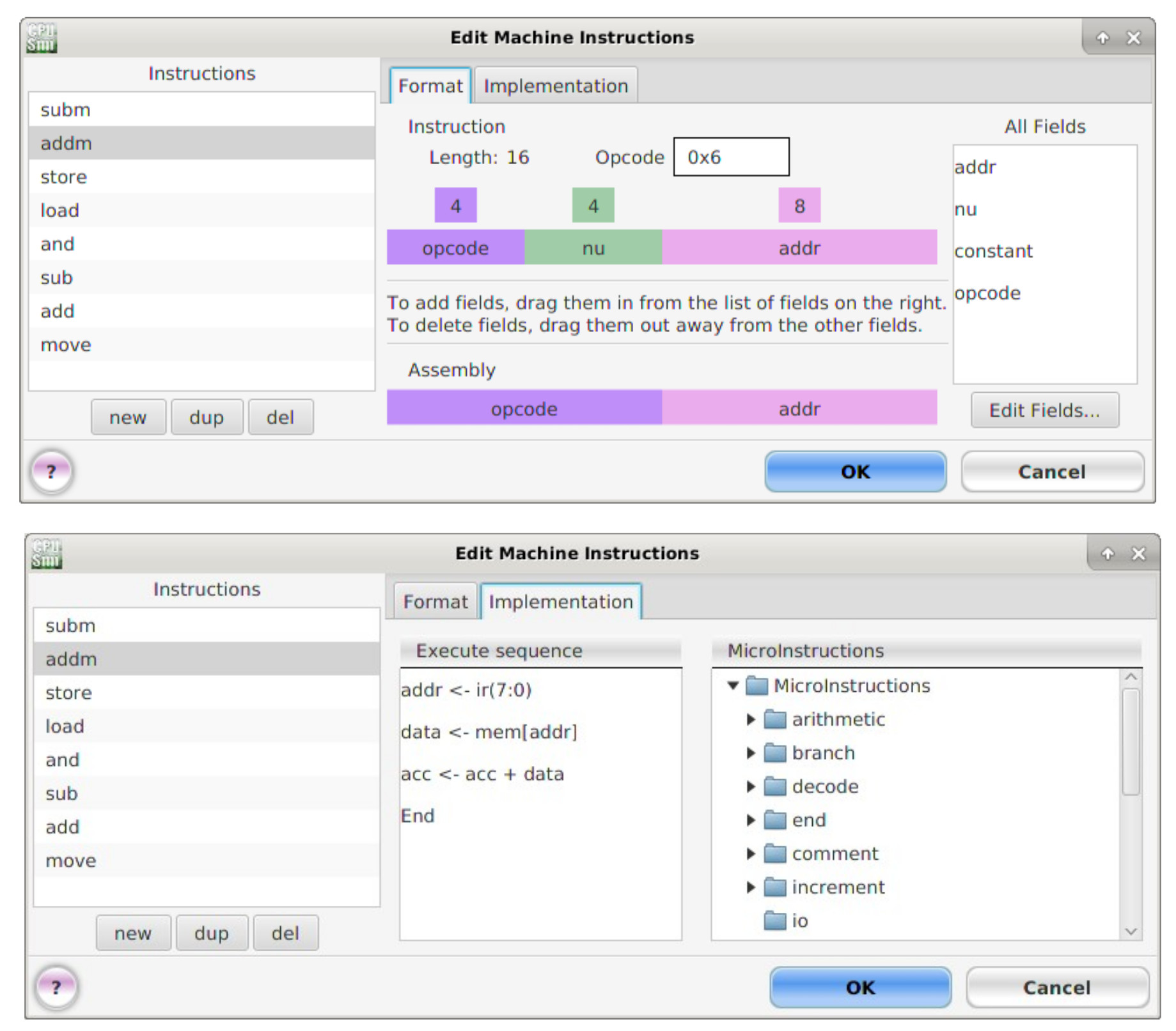
Figure 26 : ADDM machine and micro instructions.
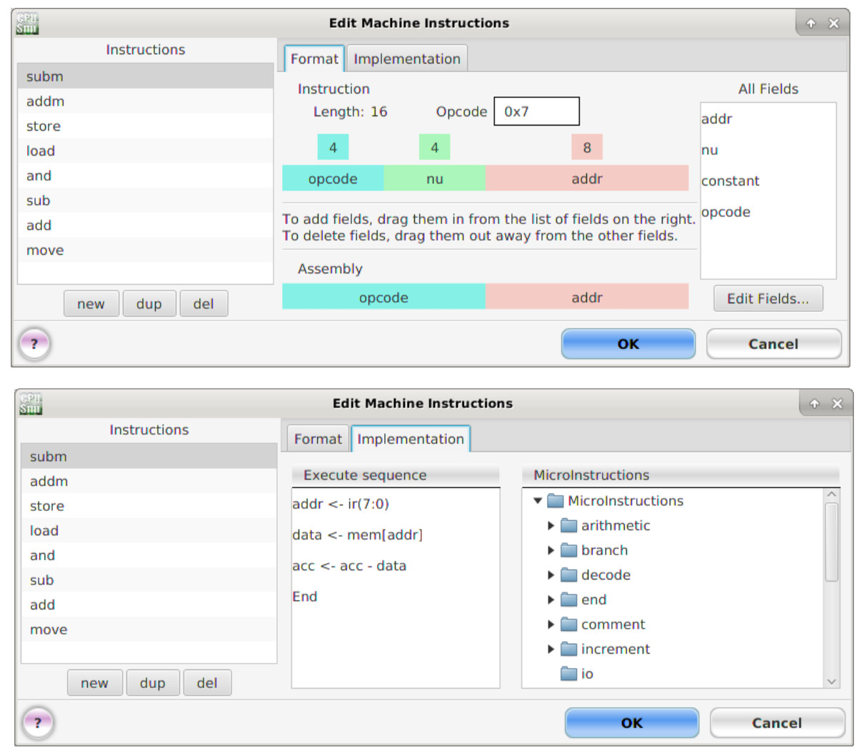
Figure 27 : SUBM machine and micro instructions.
Note, a key point to spot here is that the ADDM and SUBM instructions are essential for an accumulator based architecture to function, as they can only store one variable within the processor i.e. the ACC. Without these types of instructions a program could not perform the general purpose processing tasks show below:
X = Z + Y          LOAD  Z          ACC = Z
                   ADDM  Y          ACC = Z + Y
                   STORE X          X = ACC
The SimpleCPU computer is based on a Von Neumann architecture i.e. a stored program computer, using one memory that contains both instructions and data. This requirement causes a conflict regarding a memory location's width i.e. how many bits are stored in each location, as instructions are 16bits and data is 8bit. The number of addressable memory locations is fixed by the address bus, in this case 8bits (256 location). This gives the designer a few choices:
Software algorithms typically use loops to implement the desired sequence of operations, consider the pseudo code below:
   FOR X IN RANGE 0 TO 10		WHILE A < 123
   LOOP						    LOOP
  	DO SOMETHING				  DO SOMETHING
   END LOOP					    END LOOP
A FOR loop repeats an operations for a specified number of iterations, whilst a WHILE loop will repeat an operation until a specific event occurs. To control the flow of instruction executed, the SimpleCPU processor needs to support jump instructions i.e. instruction that will change the program counter (PC) to a specified address in memory. The flow control instructions supported by the SimpleCPU processor are shown in figure 28 below.
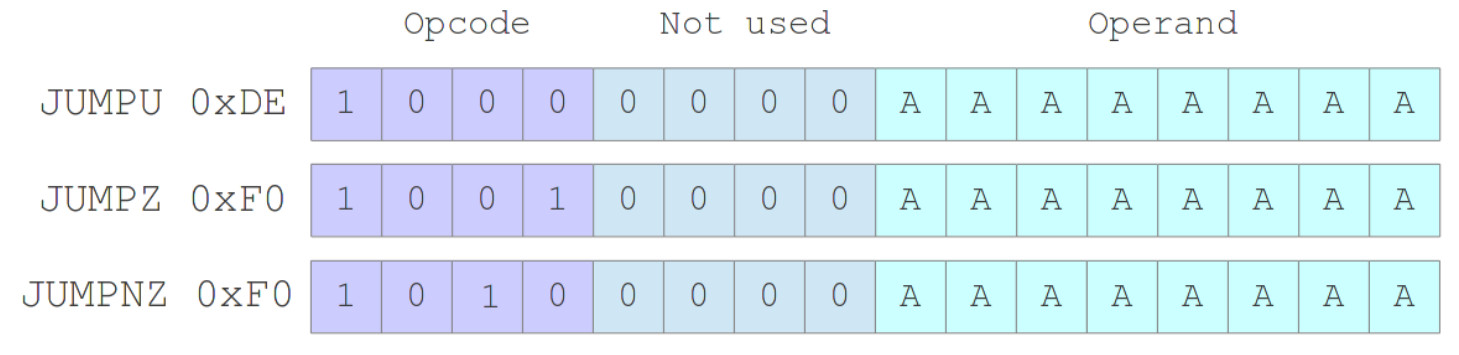
Figure 28 : Conditional and unconditional JUMP instructions.
Note, to help machine-code "readability" the top two bits of the opcode field for a jump instruction is always "10". The PC-relative addressing mode could have been used for the JUMP instructions i.e. the 8bit operand is a signed offset from the current PC, a relative jump, rather than an absolute jump address. Decided to keep the absolute addressing mode, otherwise another ADDER would be reduced.
These instructions use the absolute addressing mode i.e. an 8 bit address (A bits), used to specify the branch target location of the next instruction. There are two types of jump instructions: conditional (JUMPZ, JUMPNZ) and unconditional (JUMPU). Unconditional jumps always change the address stored in the program counter (PC) to the absolute address specified in the instruction i.e. the address of the next instruction to be executed. Conditional jumps are conditional on the state of the ACC i.e. a jump occurs if it is zero (JUMPZ) or not zero (JUMPNZ). If the jump condition is not true e.g. ACC=1 and JUMPZ instruction is executed, the PC is simply incremented to the next address PC=PC+1. The JUMPU, JUMPZ and JUMPNZ machine and micro instructions are shown in figures 29, 30 and 31.
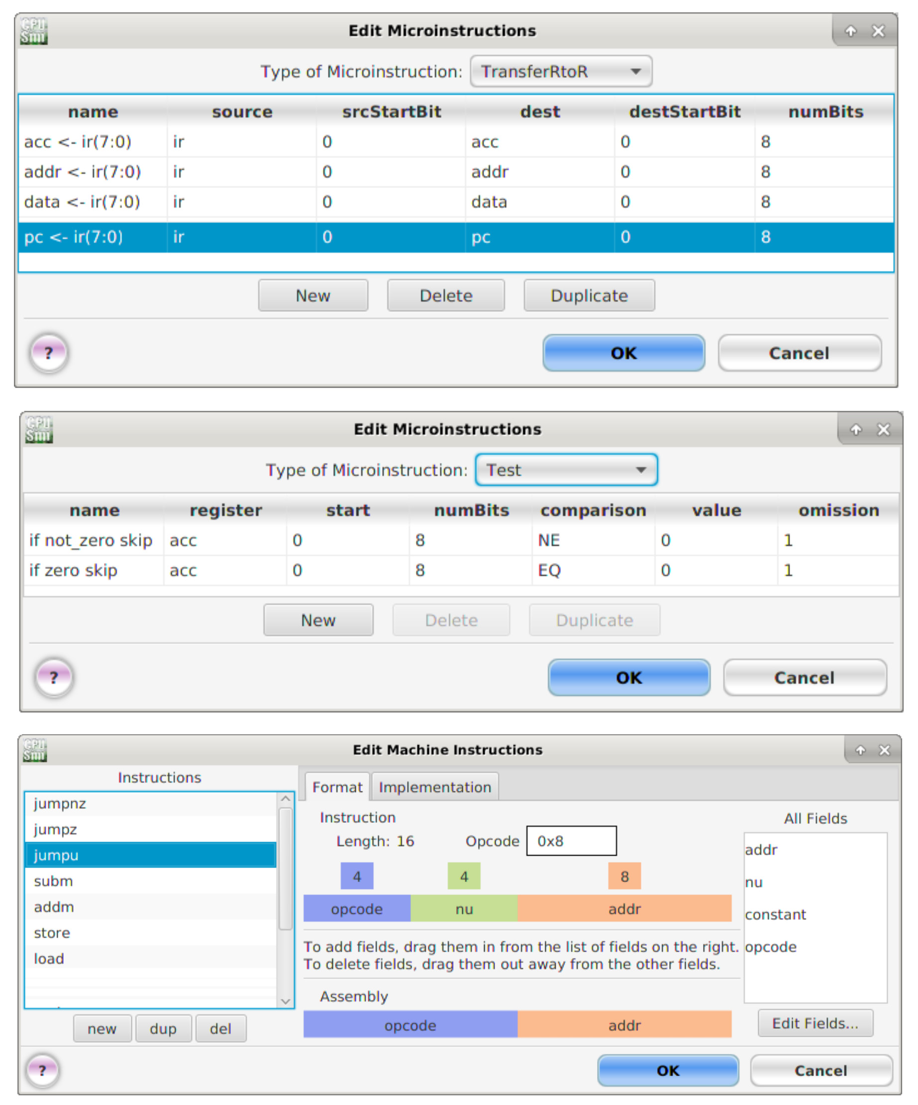
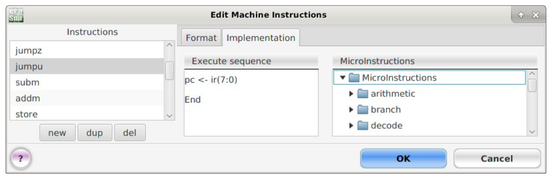
Figure 29 : Unconditional JUMP machine and micro instructions.
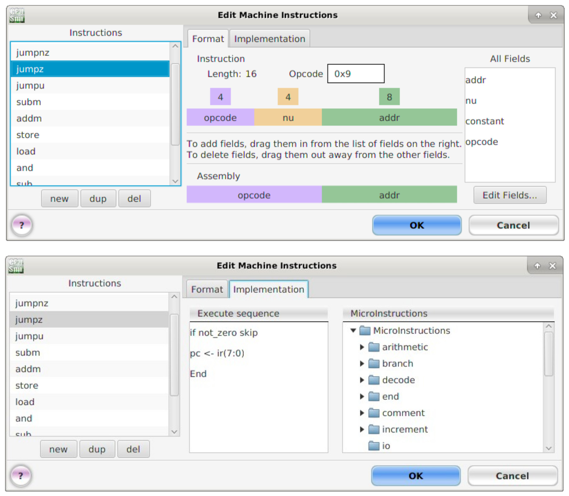
Figure 30 : Unconditional JUMPZ machine and micro instructions.
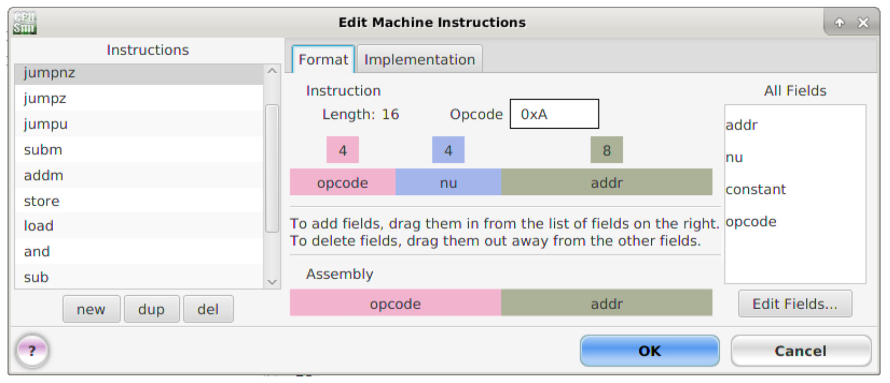
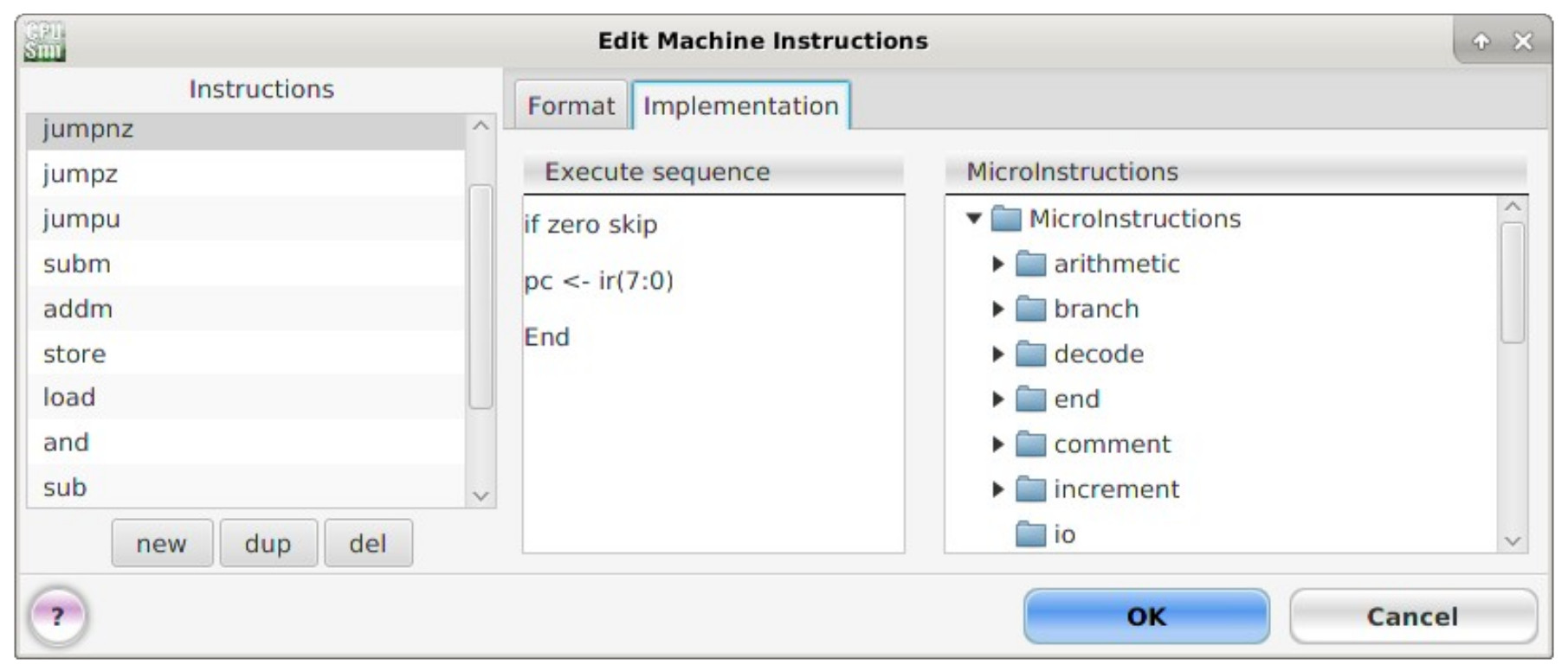
Figure 31 : Unconditional JUMPNZ machine and micro instructions.
The completed CPUSim simulation model is available here: Link. To load this machine model into the CPUSim simulator left click on the pull down menu:
File -> Open machine
selecting the simpleCPU.cpu file. Now that the processor's instructions have been defined we can write, assemble and execute the test program shown below:
start:
    move 0x00
    store 0x0D
    move 0x03
    store 0x0E

loop:
    jumpz end
    sub 0x01
    store 0x0E

    load 0x0D
    add 0x0A
    store 0x0D
    load 0x0E

    jumpu loop

end:
    jump end
Note: this program performs the calculation 10 x 3 = 30, storing the final result in address 0x0D. Multiplication using repeated addition is not best idea for large values, however, for small values its relatively efficient. When this test program has finished the processor get stuck in an infinite loop, this is intentional as there is no operating system (OS) to fall back to i.e. there is no other software running on this processor, if we don't "stop" the processor it will execute the data after this program as if they were instructions, then continue to execute unused memory, which would not be a good thing :)
To enter a new program left click on the pull down menu:
File -> New text
This will open a new edit window, enter the test code, then left click on the pull down menu:
File -> Save text
Save this program to your working directory using the file name test.a. Within this editor instruction names are highlighted in GREEN indicating that a matching machine code instruction has been found by the assembler, otherwise there is a syntax error. During a simulation you can set breakpoints i.e. select an instruction at which the simulation will pause. This requires the simulator to know which register is used as the program counter, this is done by left clicking :
Execute -> Options ...
Then click on the breakpoints tab, selecting Breakpoints and update the program counter pull-down menu, as shown in figure 32.
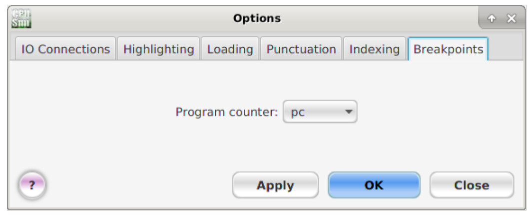
Figure 32 : Breakpoint setup.
To single step through the program at the micro-instruction level, left click on :
Execute -> Debug Mode
To assemble and load this program into memory left click on the pull down menu:
Execute -> Assemble & load
If there are no syntax errors, this will update the memory panel with the machine code values of the instructions. Change the number base of each window to hexadecimal, using the Address and Data pull down menus, as shown in figure 33.
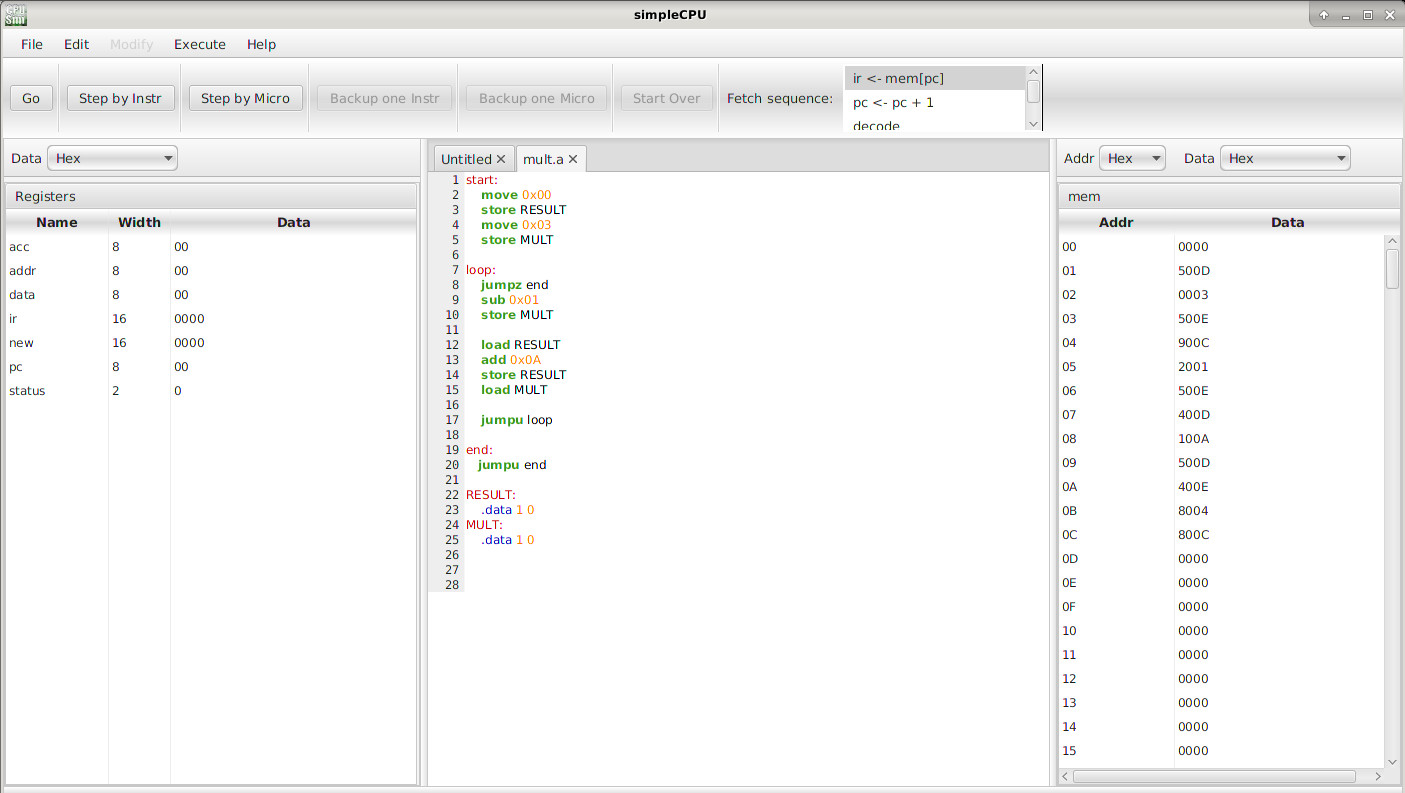
Figure 33 : RAM and register display windows.
Note, the first instruction fetched by the CPU is always from memory location 0 i.e. when the simulation is reset the PC is reset to 0. Single left click on the 'Step by Micro' button to view the different phases of the Fetch - Decode - Execute cycle and the micro-instruction used to implement them. This will highlight the micro-instruction currently being performed in the top right panel and highlight registers that are updated in the left register panel.
To simplify programming labels can be used to avoid having to use hardcoded addresses within the program as shown below and in figure 33.
MULTIPLICAND EQU 10
MULTIPLIER   EQU 3

start:
    move 0x00
    store RESULT
    move MULTIPLIER
    store MULT

loop:
    jumpz end
    sub 0x01
    store MULT

    load RESULT
    add MULTIPLICAND
    store RESULT
    load MULT

    jumpu loop

end:
    jump end

RESULT:
    .data 1 0
MULT:
    .data 1 0
Note: label can be used to identify addresses within a program e.g. the address of an instruction we want to JUMP to. They can also be used to represent variables using the .data assembler directive. This tells the assembler to reserve 1 memory location for each variable, in this case initialising it to the value 0. When assembled these labels will be replaced with the same addresses as the previous example. The advantage of this approach is that as the program grows we do not need to got back and manually update the hard-coded addresses within the program, the assembler with now do this for us. We can also define constants within the program using the EQU command, these make the program more readable, they are not variables :).
WORK IN PROGRESS

This work is licensed under a Creative Commons Attribution-NonCommercial-NoDerivatives 4.0 International License.
Contact email: mike@simplecpudesign.com