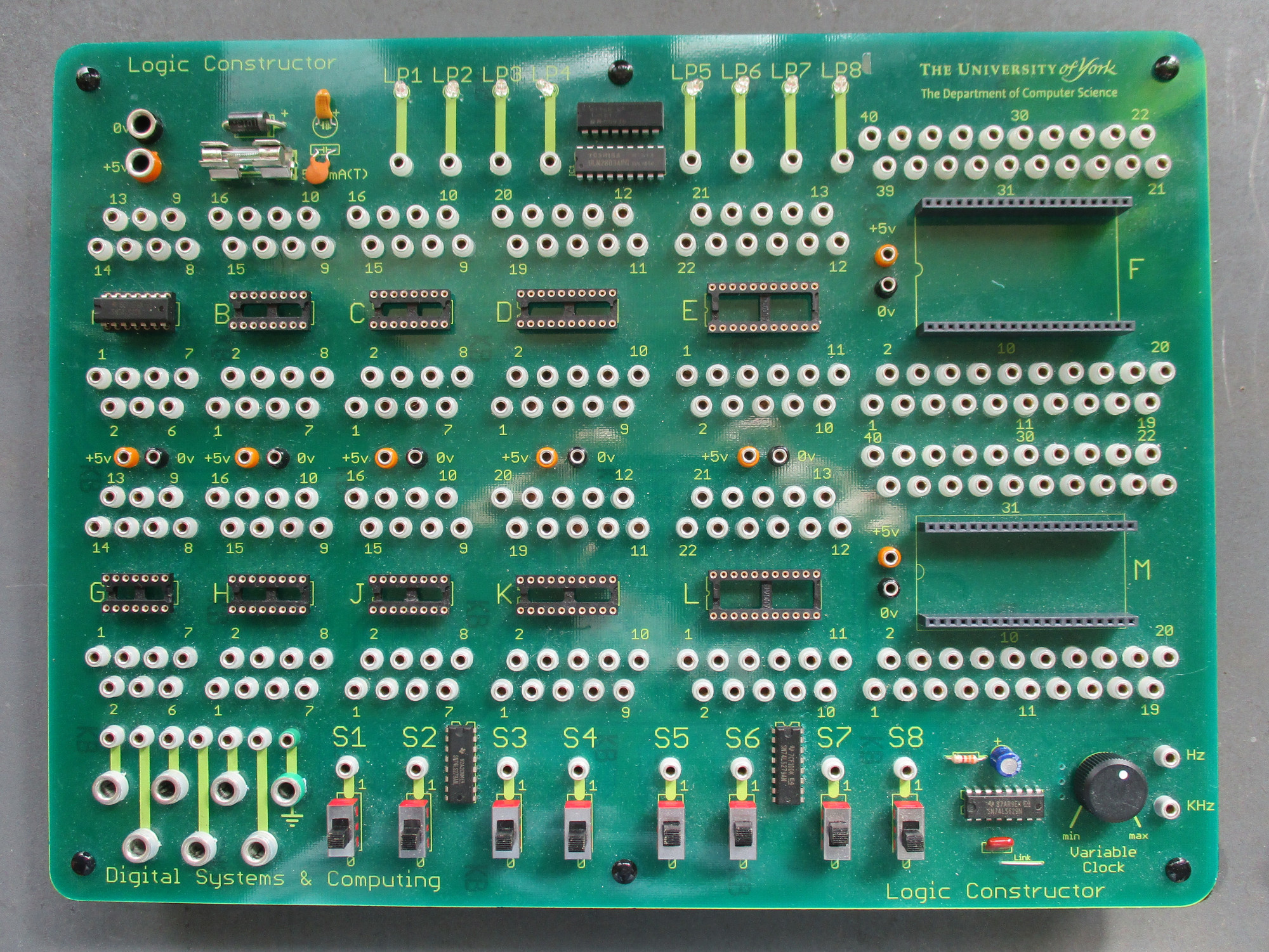
The motivation to build this TTL (Link) version of the SimpleCPU processor came around owing to the need to build a centre piece demo for open-days and a pile of Logic Constructor boards becoming available (were going to be dumped), as shown in figure 1. We used these boards when we taught electronics in our first year, but, those days are gone :(. This board is not very space efficient, but i decided to use them to construct a TTL computer as their size was a positive, allowing the construction of a "tower computer", using the boards to form the sides of the "tower". I thought this would make an interesting eye catching demo that visitor could not ignore i.e. an ice-breaker demo where people would have to stop and ask "what is this". The answer to this question and the aim of this demo is to highlight the hidden complexities within those small lumps of silicon we call a computer. To give visitors a better view of these complexities in their construction. To allow demonstrators / guides to compare and contrast the exact same processor running in a small FGPA board that people would recognise and accept as a "computer" and this towering beast that highlights what actually goes on hidden behind the scenes. Also, this is the first processor architecture students are taught in the SYS1 module i teach (implemented in the lab using an FPGA), so makes it a good choice for an openday demo i.e. links into teaching.
I confess i previously avoided making a TTL version of the SimpleCPU processor, taking the easy route and used CPLDs in the bread board implementation (Link). However, a TTL implementation is a rights of passage and has to be built :).
NOTE, this work had to be stopped owing to new H&S restructions where i work :(.
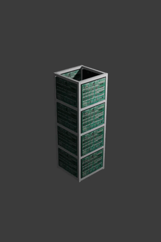
Figure 1 : Logic Constructor board (left), Tower computer (right)
7400 Logic Devices
Architecture \ Instruction-set
ALU : Arithmatic and Logic Unit
PC : Program Counter
ACC : Accumulator
IR : Instruction Register
MUX : Data and Address multiplers
Memory : RAM and ROM
DECODER : Control logic
LED : display board
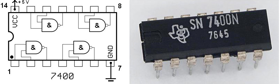
Figure 1 : Logic Constructor board
Come world war 3, or the zombie apocalypse, two things will survive cockroachs and systems built with 7400 logic devices (Link). The 7400 logic series came to power in the 1970s, when third generation computers ruled the earth. Originally these ICs e.g. AND, OR, XOR gates etc, were constructed using Transistor-Transistor Logic (TTL) (Link), but later were "updated" to use Complementary Metal Oxide Semiconductor (CMOS) (Link). Personally, i always found the TTL versions almost indestructible, surviving many a mistake. The CMOS version are also very forgiving when compared to modern silicon. However, with big transistors comes "big" costs, and these devices are becoming harder and harder to source. Basic logic gates and buffers are still readily available, pin through board and surface mount versions are easy to obtain. However, the more exotic flavours are now only available on the second-hand market e.g. the 74181 4-bit ALU (Link), shown in figure 2.
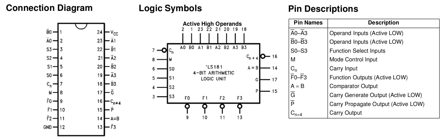
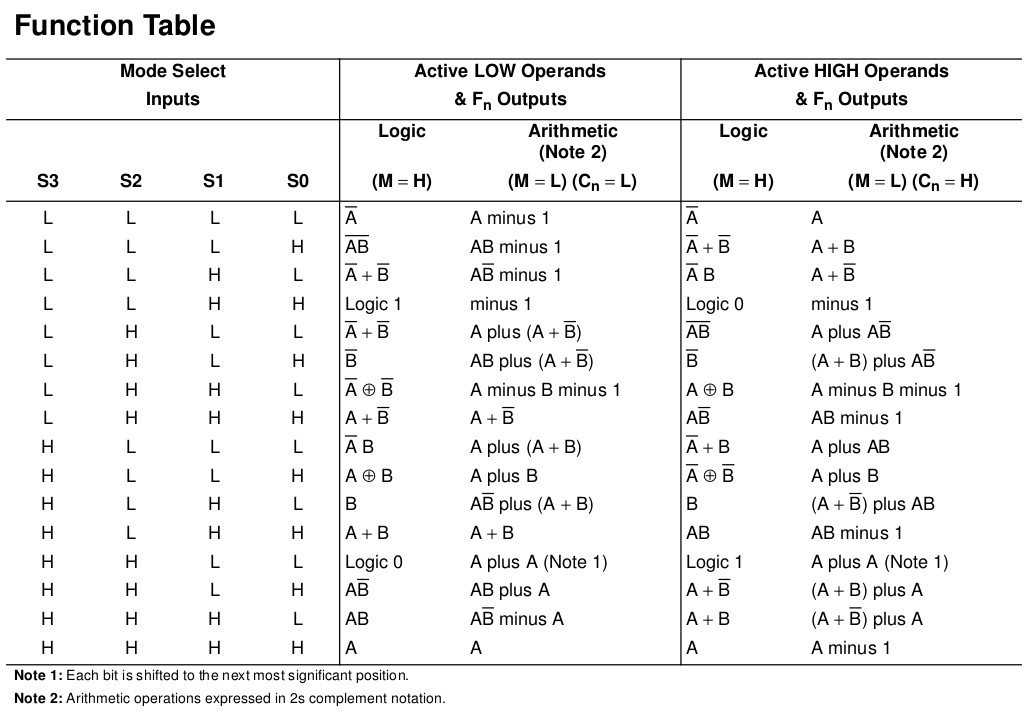
Figure 2: 74181 4-bit ALU
For a typical 7400 device, this ALU version used a lot of silicon and would definitely be an option to implement this processor's ALU. However, owing to their short supply, i decided to only use ICs that are still available from main stream suppliers. Therefore, to implement this computer i will be using the following ICs:
The final two ICs in this list are the memory: EPROM for instruction memory and RAM for data memory. These are also getting harder to source, but i have a big box of these from modules long past :).
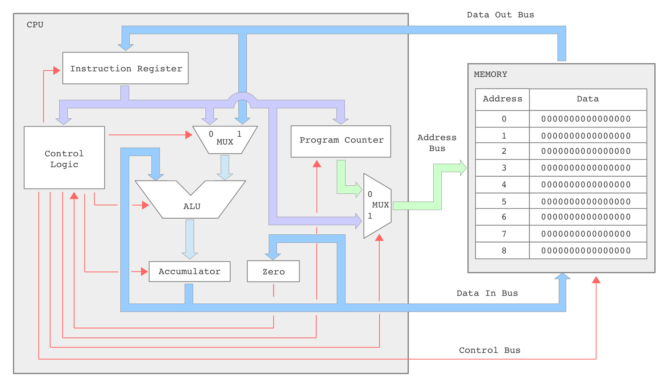
Figure 3 : simpleCPU v1a architecture
This is the first processor students are taught in the SYS1 module i teach, so makes it a good choice for an openday demo i.e. links into teaching. To simplify hardware construction this version of the processor has a very limited instruction-set, supporting 9 different instructions, shown below (assembly-code : machine-code).
In this instruction syntax X=Not-used, K=Constant and A=Address. The complexity of an instruction is also defined by its addressing mode i.e. not just how much number crunching it does, but how it fetches its operands (data). Again, to simplify the required hardware these instructions are limited to simple addressing modes:
The ALU's implementation is basically the same as the FPGA's version (Link), shown in figure 4. However, to save some space i decided to implement the MUX using tri-state buffers, as building these MUXs from logic would need a significant number of ICs. This tri-state implementation is not strictly speaking "good" design practice as i'm not allowing a "turn-around" time when enabling \ disabling the 74245 buffers i.e. there is a possibility that two drivers could drive different logic values onto the same wire at the same time. However, for the purposes of this demo its good enough (fingers crossed) i.e. the illegal drive state will only be true for a short period of time. The final TTL implementation is shown in figure 4. The eagle schematic file is available here: (Link).
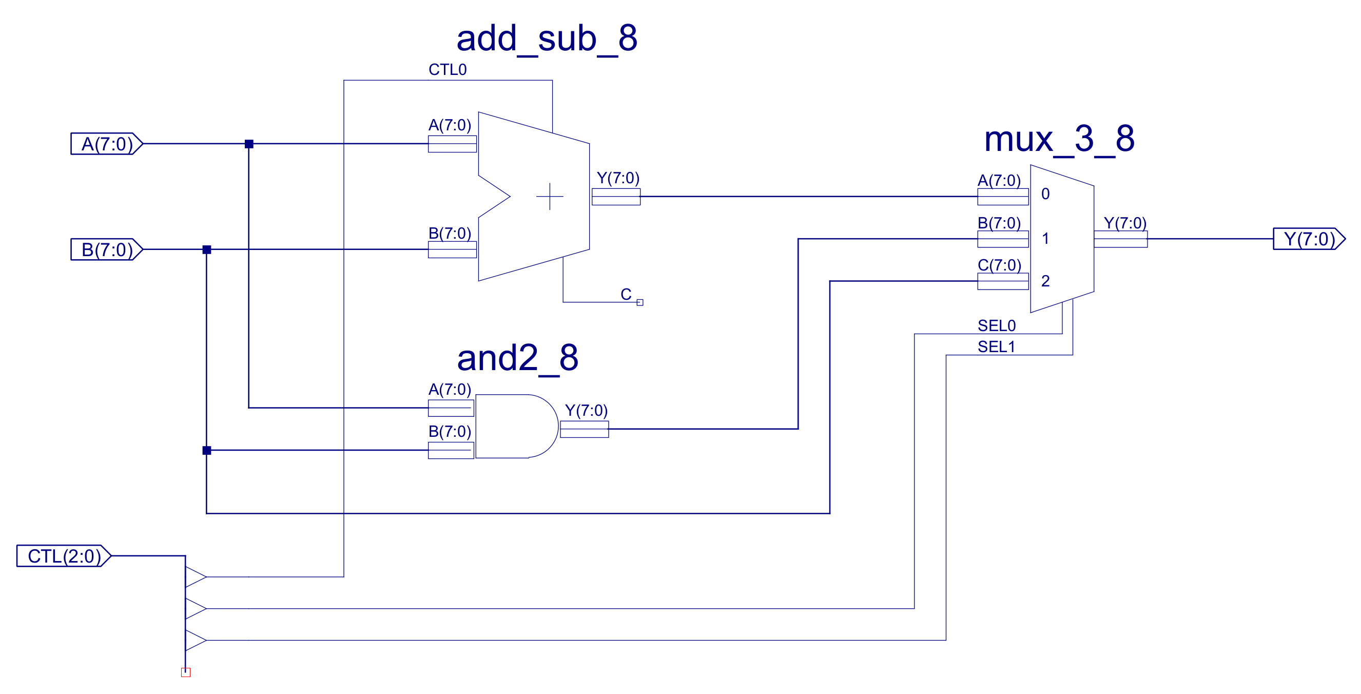
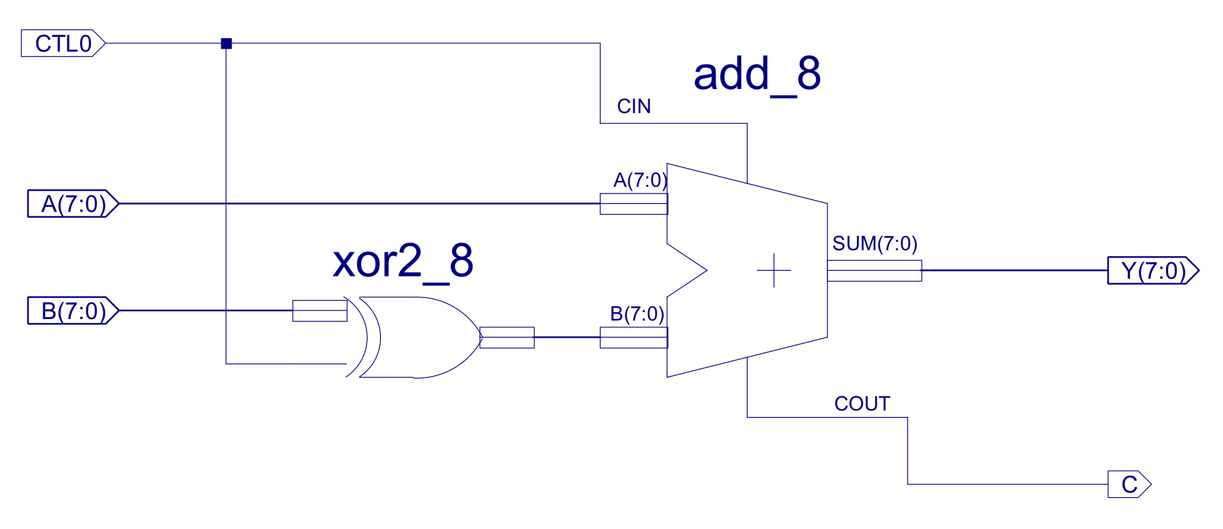
Figure 3 : FPGA ALU (top), ADD_SUB (bottom)
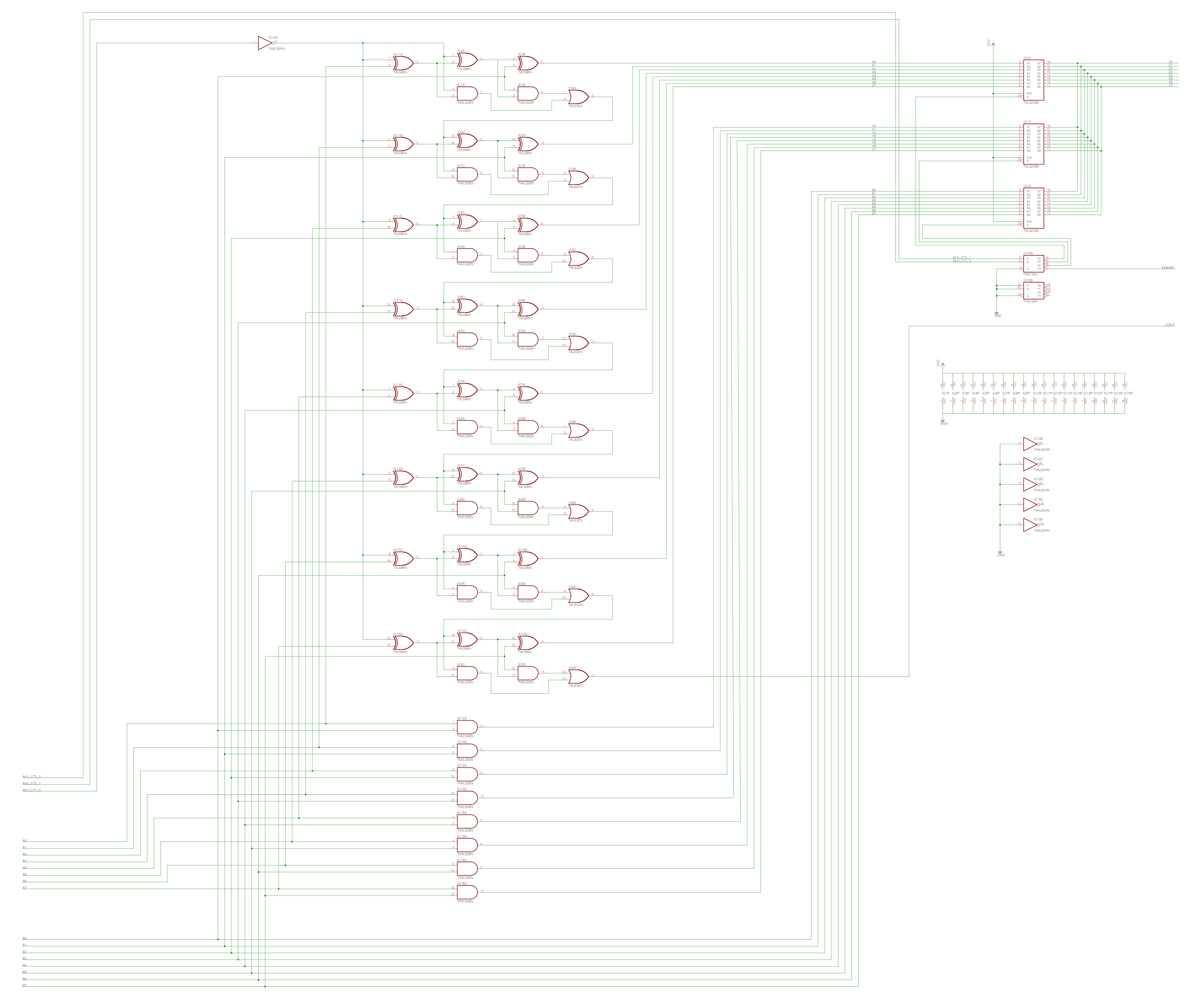
Figure 4 : ALU schematic
Looking at the block diagram in figure 3 we can see that multiplexers are used throughout the processor. A small issue with that is that these 8bit multiplexers use 20pin ICs and we only have two of these sockets per Logic Constructor. Therefore, as the multiplexer function is a fundamental building block i decided to create a daughter board. The schematic and PCB layout of this module is shown in figure 5. Note, another advantage of this approach is it helps reduce the amount of wiring, making this implementation a little more compact.
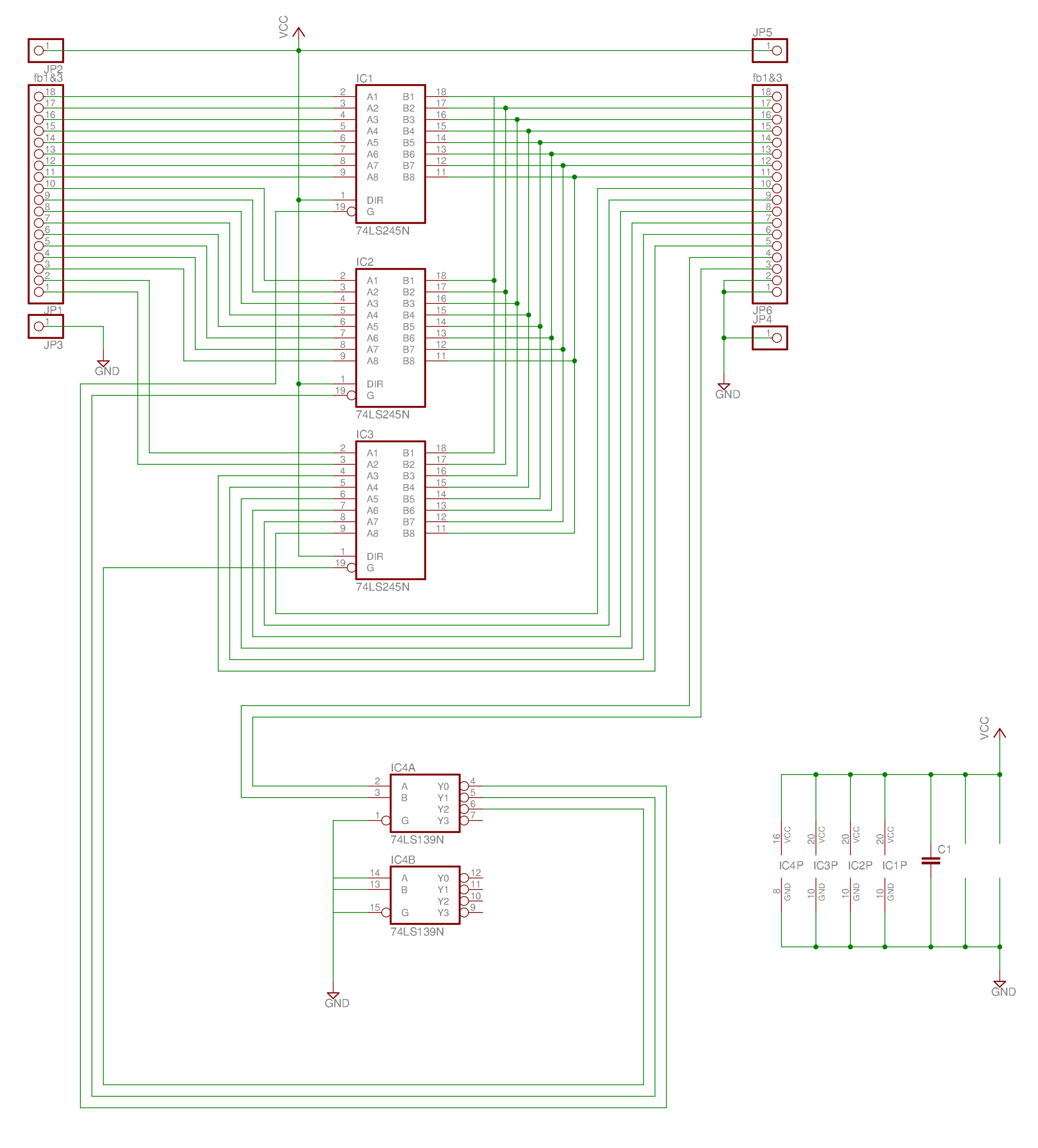
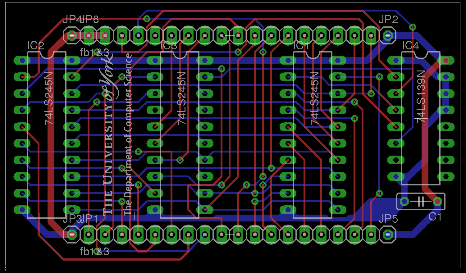
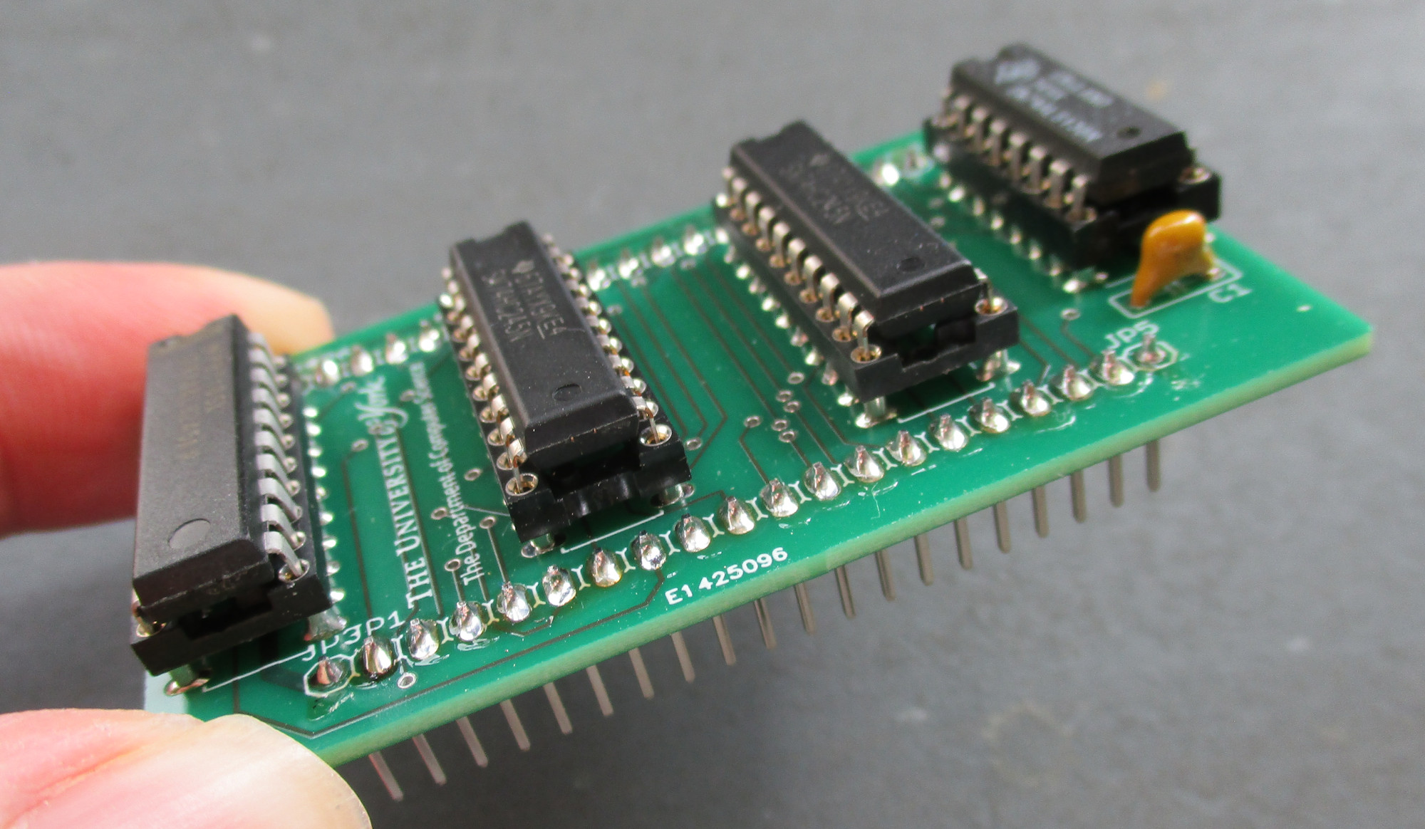
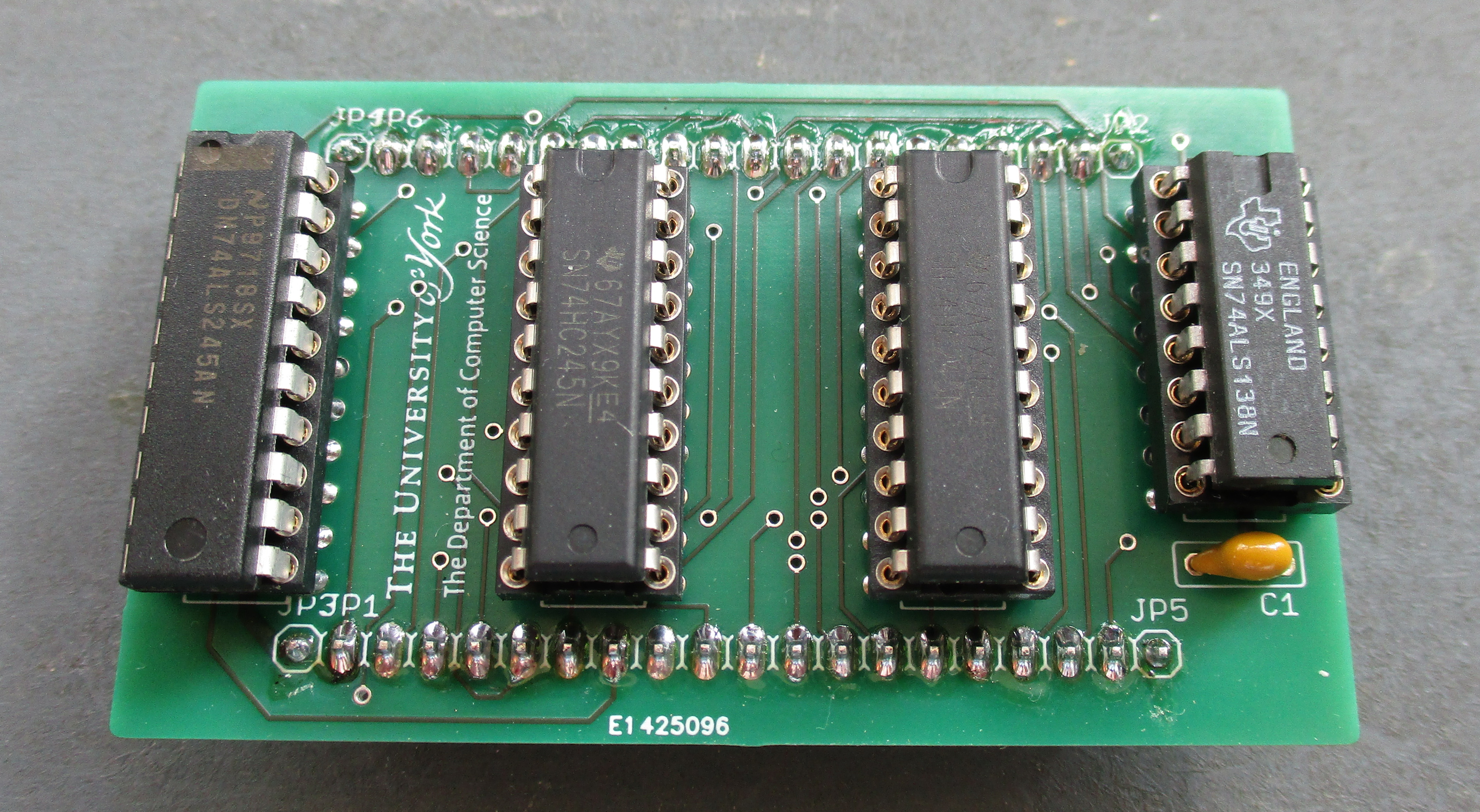
Figure 5 : Multiplexer module
This board fits into the general purpose 40 pin header located in the top left of the Logic Constructor (originally used for a CPLD board). The inputs and outputs of this board are listed below and shown in figure 6.
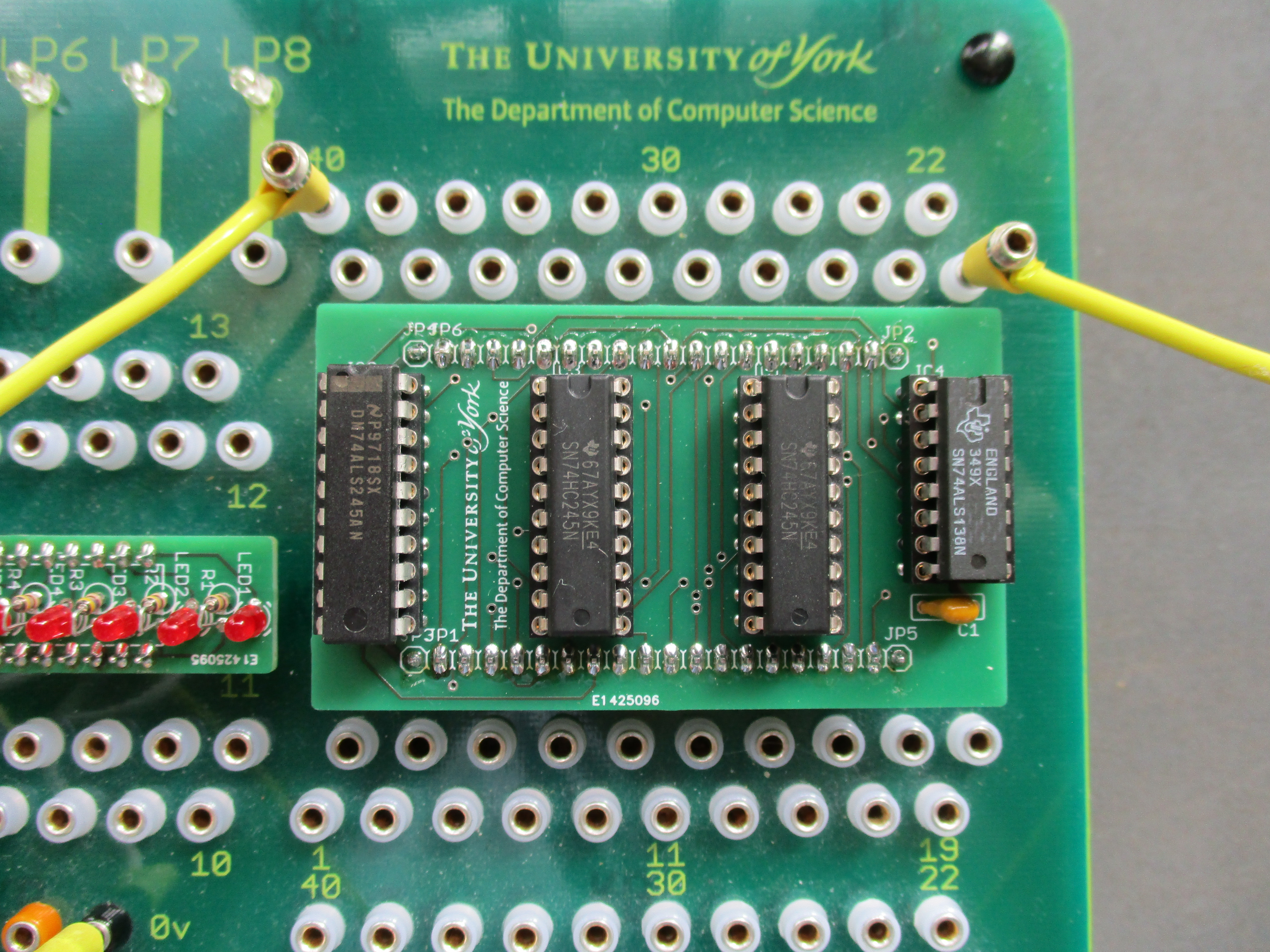
Figure 6 : Multiplexer module pins
The program counter is made from the same basic building blocks as the ALU i.e. an adder and a multiplexer, but also some memory. As one of the inputs to the adder has a fixed value i.e. 1, this simplifies this hardware down to an incrementer i.e. AND and XOR gates. Like the previous addition hardware this is a ripple adder, therefore, the critical path delay is a little longer than some designs. However, speed was never a design consideration for this machine :). The FPGA and TTL implementations are shown below:
Figure 7 : FPGA PC
Figure 8 : PC schematic
Note, the schematic implementation is the program counter (PC) and the Address MUX shown in the block diagram in figure 3. Again, the selection of the PC's input and output data are constructed using tri-state MUXs to save space. To further save space the two tri-state buffers ICs 5 and 6 in the schematic shown in figure 7 are implemented using the MUX module board shown in figure 5. This allows the PC to be implemented on one Logic Constructor board i.e. limited to two 20 pin ICs per board. Therefore, the control signals to this board will be a little different than the FGPA design.
A very simple board, an 8bit register and a 8bit NOR to implement the zero detect.
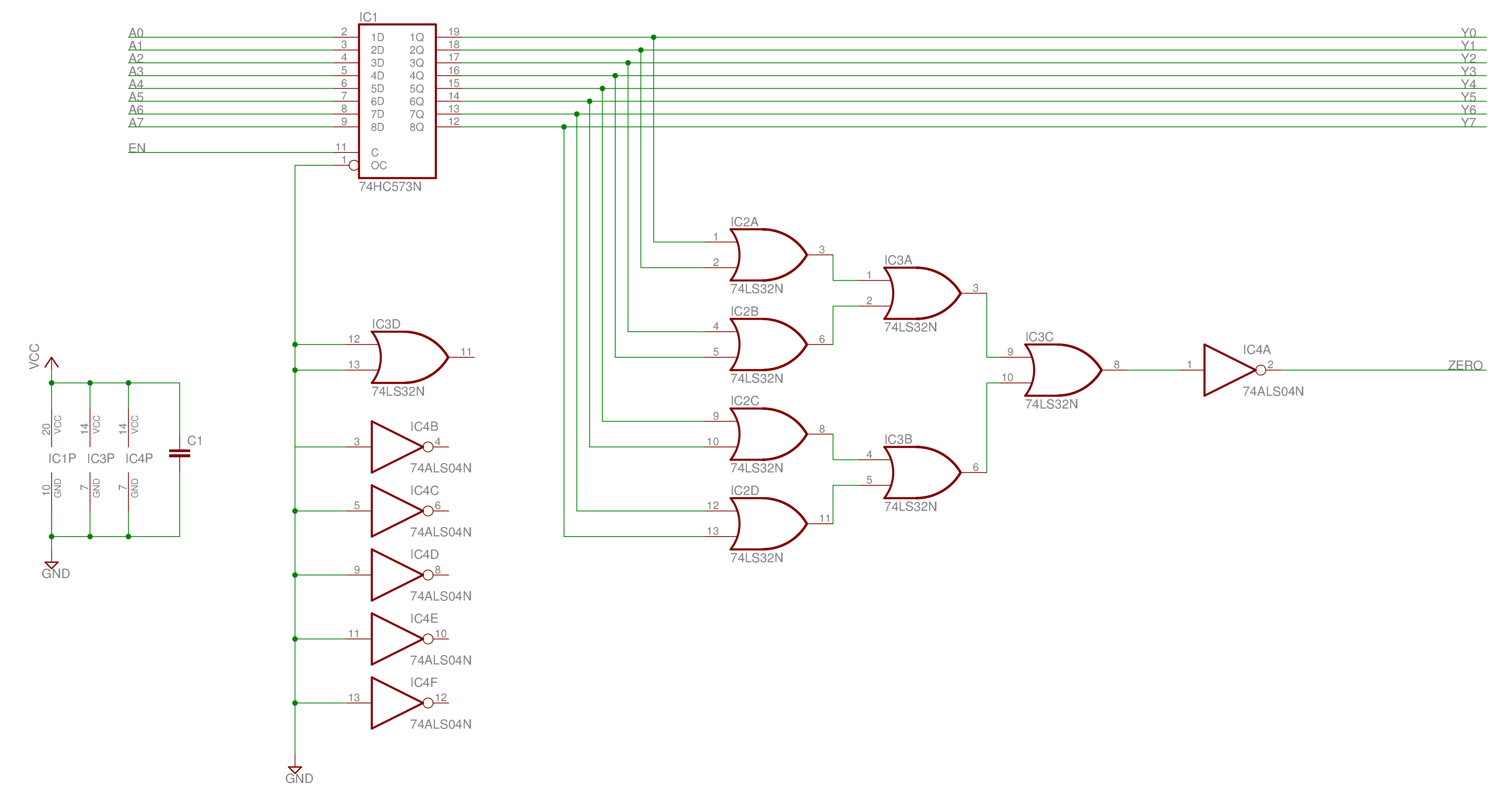
Figure 9 : ACC schematic
Like the ACC another very simple board, basically two 74573s (Octal D-Type Flip-flop) ICs, forming the 16 bit instruction register (IR). Also included on this board is the DATA MUX that selects operand data for the ALU i.e. 8bit immediate stored in IR or 8bit data from extermal RAM. Again, to save space these tri-state buffers will be implemented using the MUX daughter board.
The DATA MUX is incorporated into the instruction register (IR) board. The ADDR MUX is incorporated into the program counter (PC) board. These will be implemented using the MUX daughter board shown in figure 5.
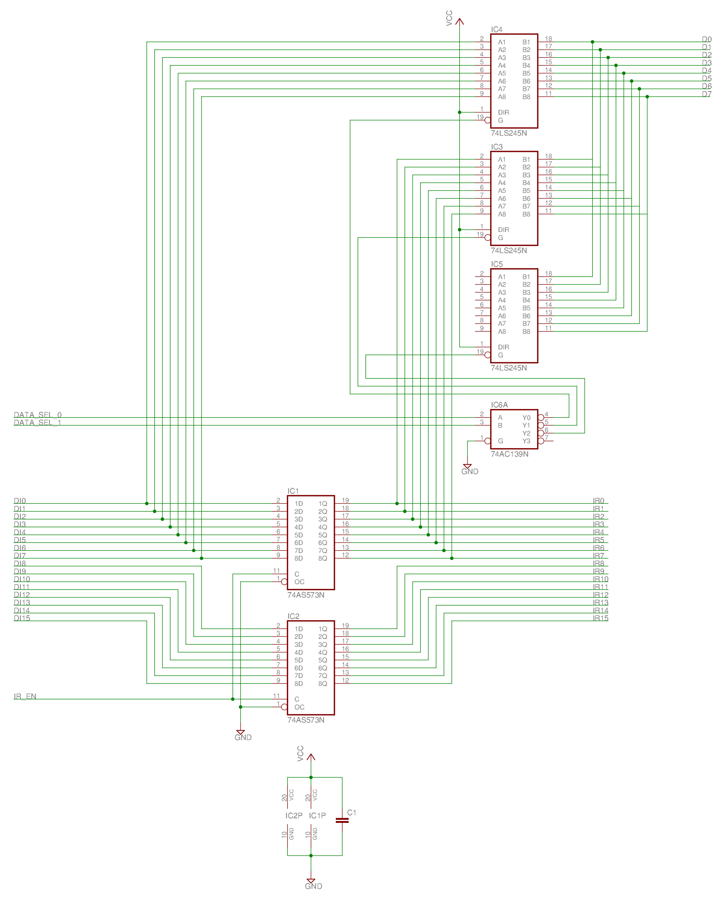
Like the previous bread board version of this computer instruction memory is implemented using 2764 EPROMs i.e. each 16bit instruction is stored across two ICs. Data memory using a 6264 SRAM. These ICs both use a 28pin socket, unfortunately the Logic Constructor boards do not have 28pin sockets :(. Therefore, i designed a second daughter board as shown in figure 11.
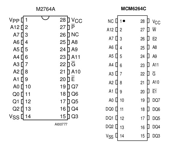
Figure 10 : 2764 (EPROM) and 6264 (SRAM)
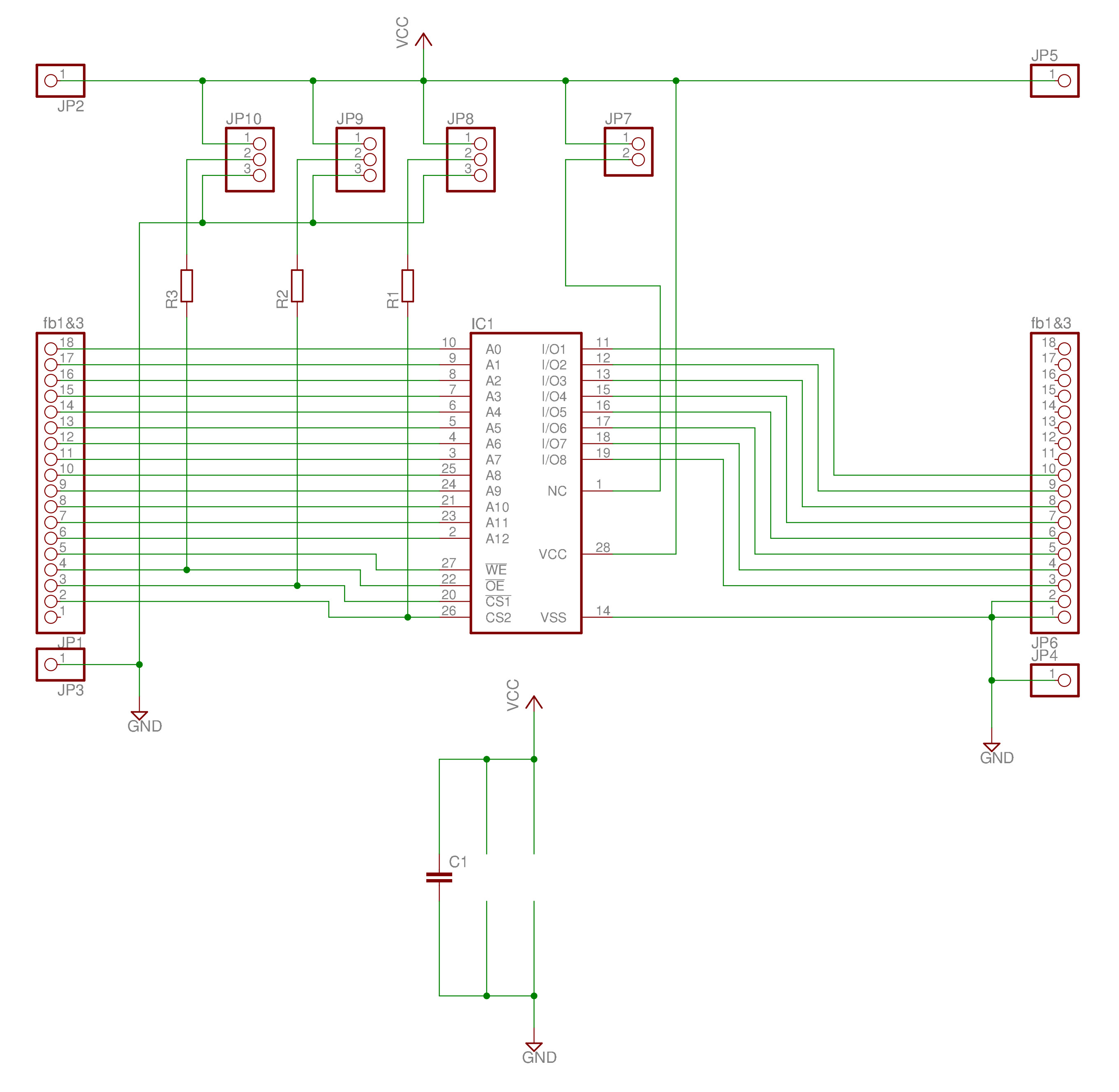
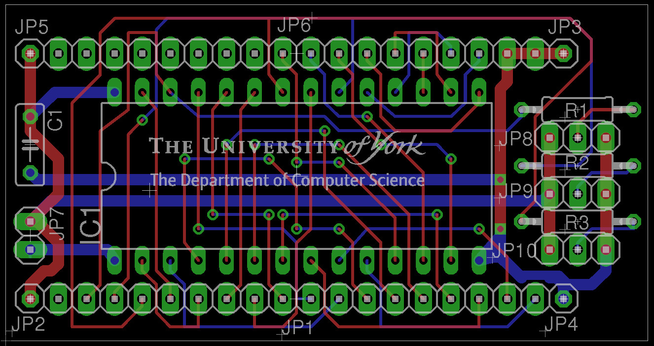
Figure 11 : Memory module
As the two memory ICs have basically the same pin-out, this module can be used by both ICs, where needed jumpers are used to disconnect, or tie high / low specific pins.
The inputs and outputs of this board are listed below :
The complete memory implementation is shown in figure 12.
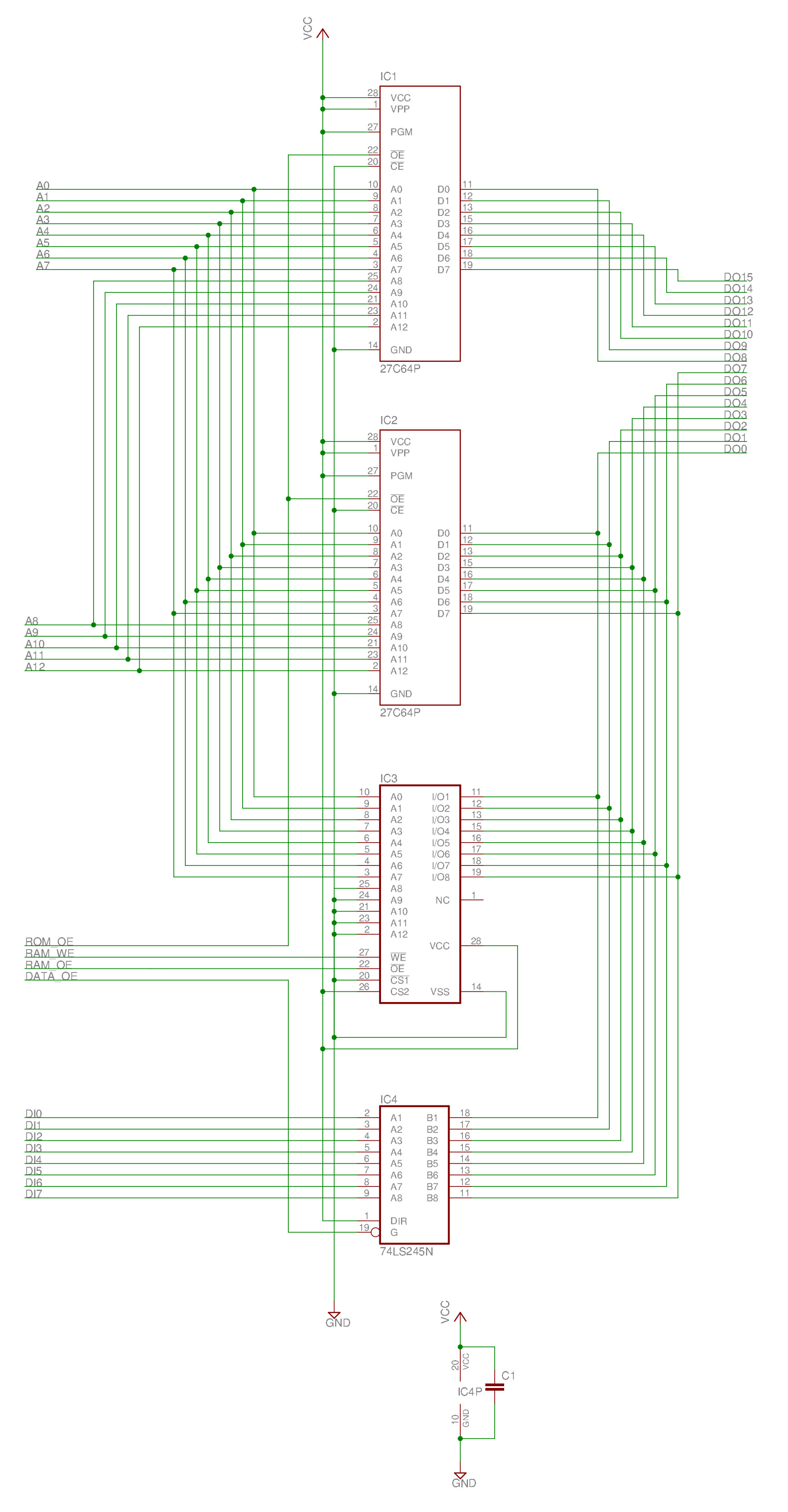
Figure 12: Memory
The control logic / instruction decoder is made up of a a number of different elements. Like the FPGA implementation the instruction state is represented in the processor using a ring counter, as shown in figure 13.
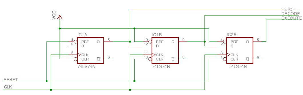
Figure 13: ring counter
The instructions decoder's binary to one-hot decoder is implemented using two 74138 decoders, as shown in figure 14.
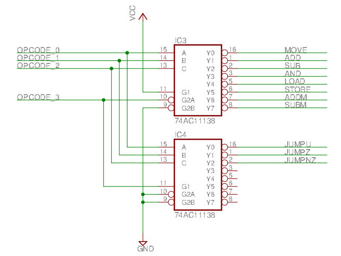
Figure 14: binary to one-hot decoder
The control logic combines the instruction decoder's one-hot output with the ring counter state to implement the micro-instructions needed to implement each machine level instruction. This logic is basically the same as FGPA version, but with a couple of small modifications owing to the different multiplexers used.
74139 DECODER
G B A Y0 Y1 Y2 Y3
1 X X 1  1  1  1
0 0 0 0  1  1  1
0 0 1 1  0  1  1
0 1 0 1  1  0  1
0 1 1 1  1  1  0

ALU_CTL_0 : ADD=0, SUB=1
ALU_CTL_1 : 74139 A INPUT
ALU_CTL_2 : 74139 B INPUT

ALU_CTL_2  ALU_CTL_1  OUPUT
0          0          ADD / SUB
0          1          AND
1          0          PASS THROUGH
1          1          DISCONNECTED - HIGH IMPEDANCE

ADDR_SEL_0 : IR BUFFER OE
ADDR_SEL_1 : PC REG OE

PC_SEL_0 : 74139 A INPUT
PC_SEL_1 : 74139 B INPUT
PC_EN    : PC REG CLK

PC_SEL_1  PC_SEL_0  OUTPUT
0         0         IR
0         1         PC+1
1         0         DISCONNECTED - HIGH IMPEDANCE
1         1         DISCONNECTED - HIGH IMPEDANCE

DATA_SEL_0 : RAM
DATA_SEL_1 : IR

DATA_SEL_1  DATA_SEL_0  OUTPUT
0           0           RAM
0           1           IR
1           0           DISCONNECTED - HIGH IMPEDANCE
1           1           DISCONNECTED - HIGH IMPEDANCE
The "complete" control logic schematic is shown in figure 15. However, at this time its not tested :).
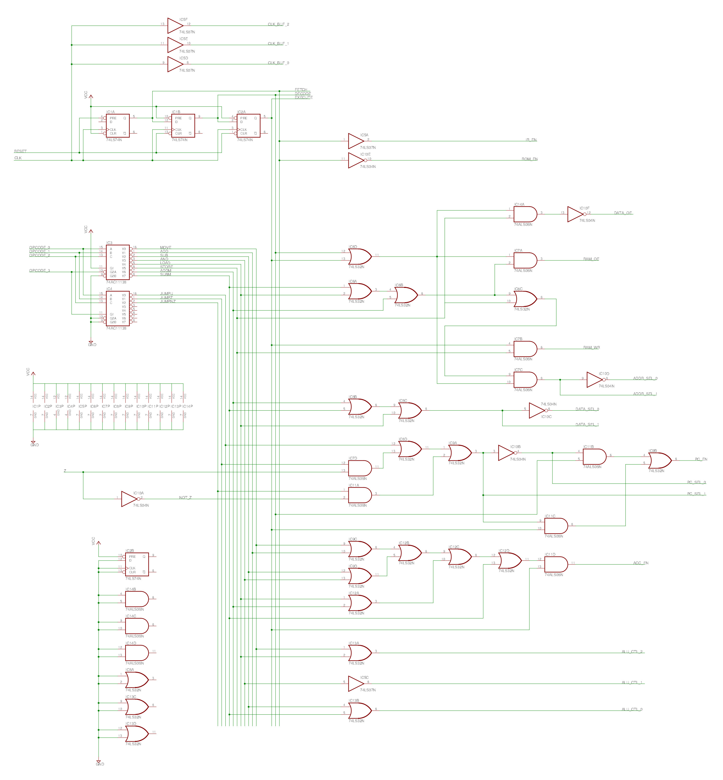
Figure 15: Decode
To help will debugging and to maximise the visual impact of the demo you need lots of LEDs. The logic constructor board does come with 8 LEDs, but to increase this LED count and make use of the 22 pin IC holder (not many chips use this foot print) i made a simple non-buffered LED boars as shown in figure
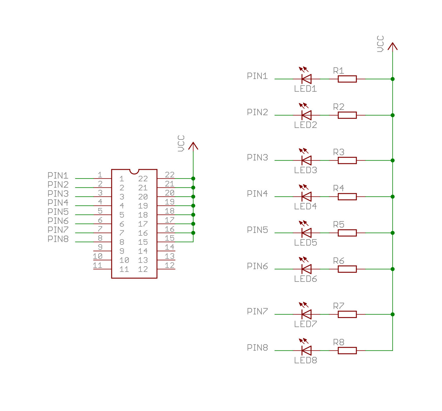
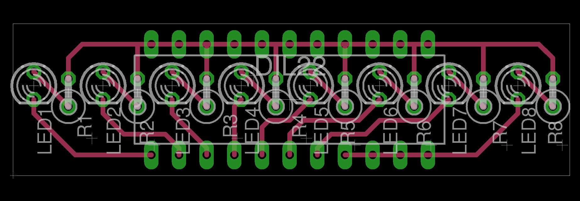
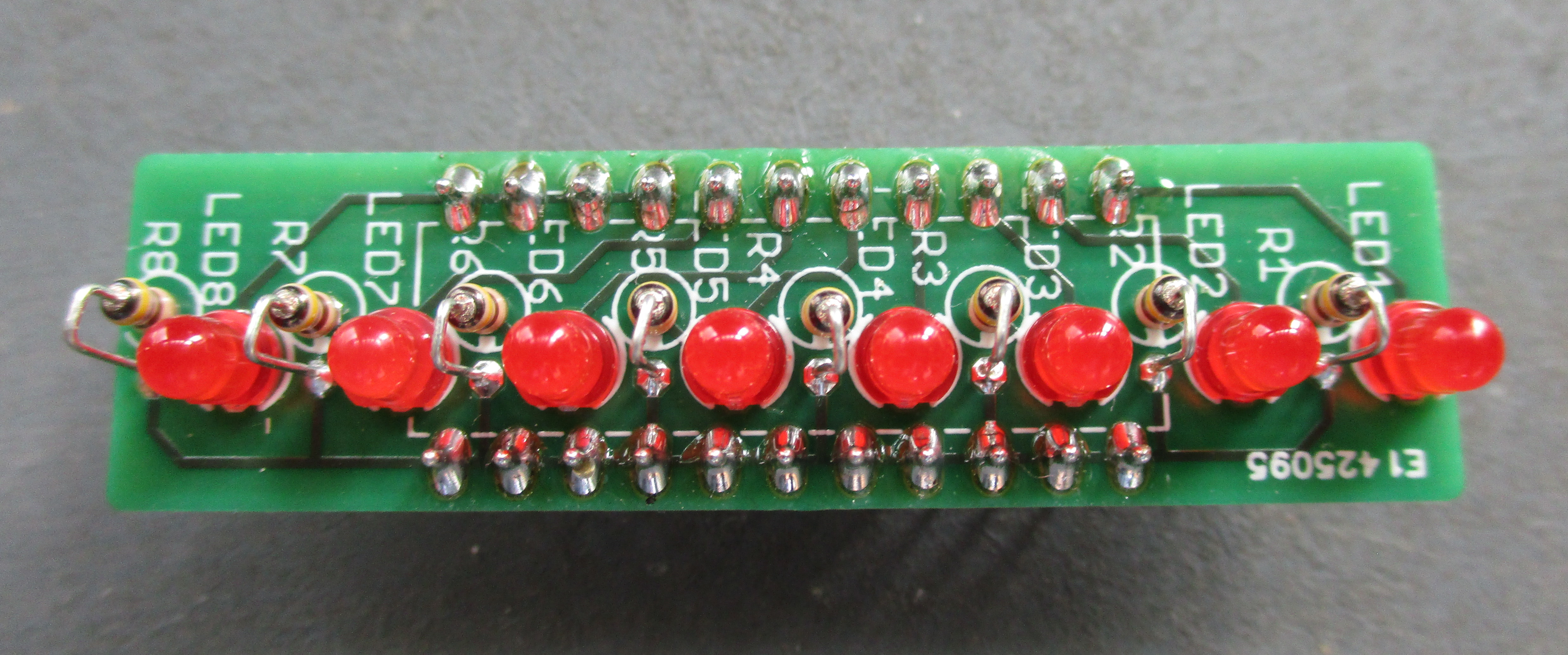
Figure : LED board

WORK "IN PROGRESS", welllll, not quite true work is paused whilst the department tries to sort out the H&S issues, to be honest its been 2 years now, so i'm not expecting this work to be completed any time soon :(.
This work is licensed under a Creative Commons Attribution-NonCommercial-NoDerivatives 4.0 International License.
Contact email: mike@simplecpudesign.com