
Figure 1 : simpleCPU_v1d block diagram
We are almost there, the SimpleCPU version 1d (Link) has almost made the jump from teaching example to a processor that can be use to do useful work. To put the processor to the test i decided to do some image processing, as the algorithms used are reasonable complex, both in terms of software structures and data types used. Another, advantage of using these test cases is that you can start to see how the pseudo code used to describe these algorithms is converted from an abstract, high level representation into its low level, assembly language implementation. Highlighting the typical problems faced by any processor designer i.e. matching the hardware to the software's requirements. Also, you get visual feedback of any errors, that helps debug and could also produce the next master piece for Tate Modern :).
The new and improved ISE project files for this processor can be downloaded here: (Link), basically the same structure, but with a few tweaks and improvements needed for the image processing. An updated python based assembler is also available here: (Link).
What is an image?
Memory
Data processing
Hardware
Software
Before we can start we need to decide how we are going to represent images in the computer? There are actually quite a few way of representing the different colours we see in an image, each with its own advantages and disadvantages. I'm definitely not an image processing guy so can not comment on these too much, but you can find out more here:(Link). Perhaps one of the most common models used is the RGB colour model (Link), where each colour is defined as a mixture of the three primary colours RED, GREEN and BLUE, as shown in figure 2.
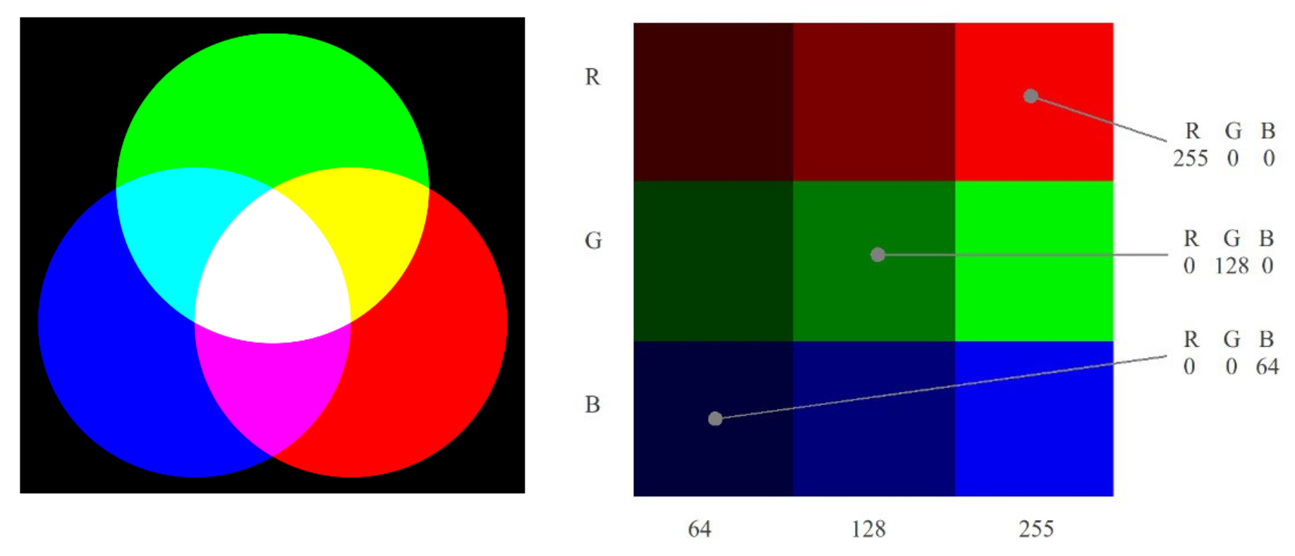
Figure 2 : RGB colour model
In this example we have the three primary colours: red, green and blue, the overlap of these colours produce the secondary colours: yellow, cyan and magenta. The addition of all three colours produces white, the absence of all three colours produces black, varying the intensities of these primary colours will produce all the colours of the rainbow :). To represent the colour of each picture element, or pixel, we need to store its R, G and B values. The intensity of these colours are typically represented by an 8-bit value i.e. 0=none, 255=full. Therefore, to store this data in memory we will need 8+8+8 = 24 bits for each pixel. The nine pixel image (3×3) is shown in figure 2, would require 9 x 24 = 216 bits, or 27 bytes. Note, in this example each row is a different primary colour, varying in intensity: 64, 128 to 255.
The other colour model ive used in the past is YCbCr (Link), typically used in CMOS image sensors (Link), as show in figure 3. Here we represent each pixel's colour as its "brightness", luminance (Y) and two chroma components (CB and CR). Note, cheap USB web cameras are not really an option for the simpleCPU i.e. toooo much work to implement the USB stack. However, the type of image sensor shown in figure 3 typically use a serial I2C bus (Link) for config/control data and a parallel data bus to transfer image data. This is relatively easy to implement in hardware and will be a later addition to the simpleCPU product line :).
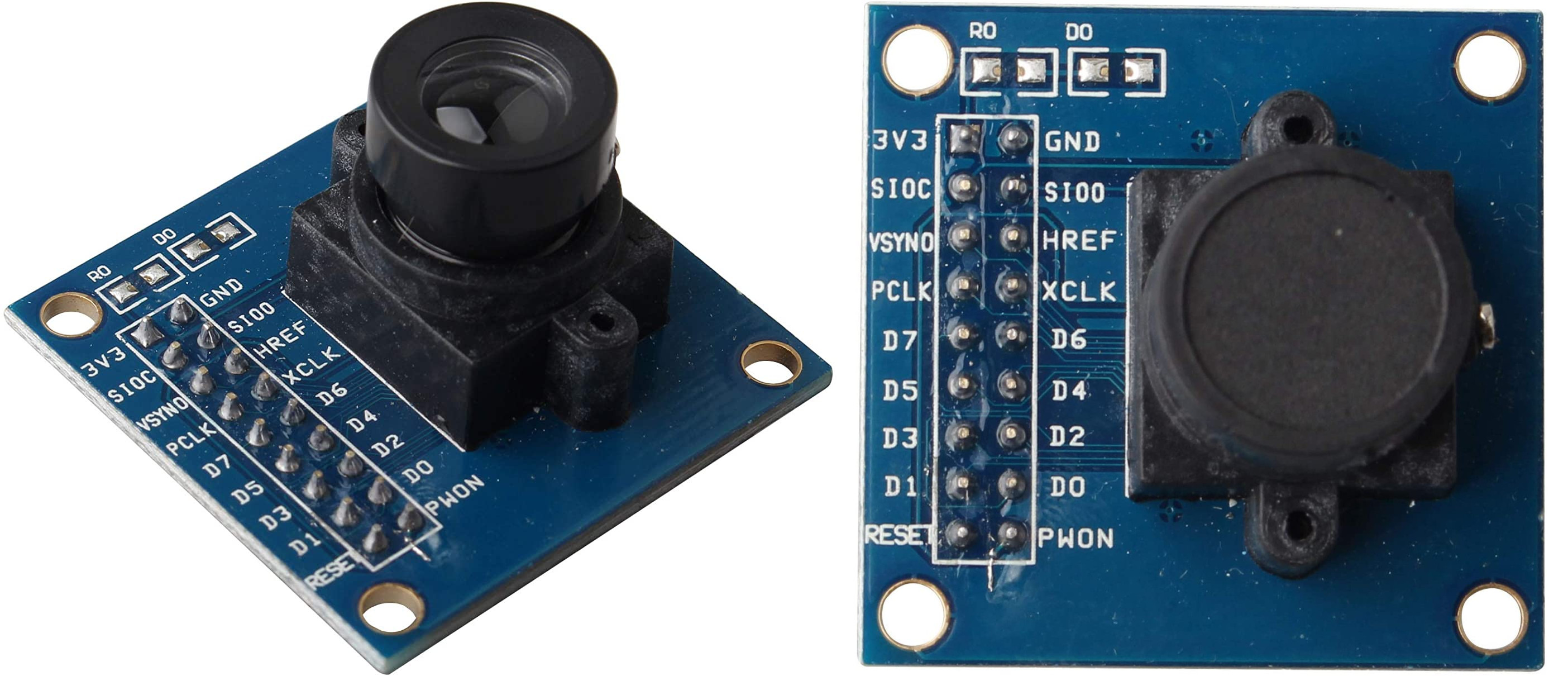
Figure 3 : CMOS image sensor
For the present test system ive assumed that we have already captured an image and stored it in memory. Note, i need to port the existing camera controller i made for a different project, but ive not had time :(. However, one thing you soon realise when processing images is that you need a lot of memory to store this type of data. Only having 4096 x 16-bits of memory space does put some limitations on what we can do, consider the examples shown in figure 4.
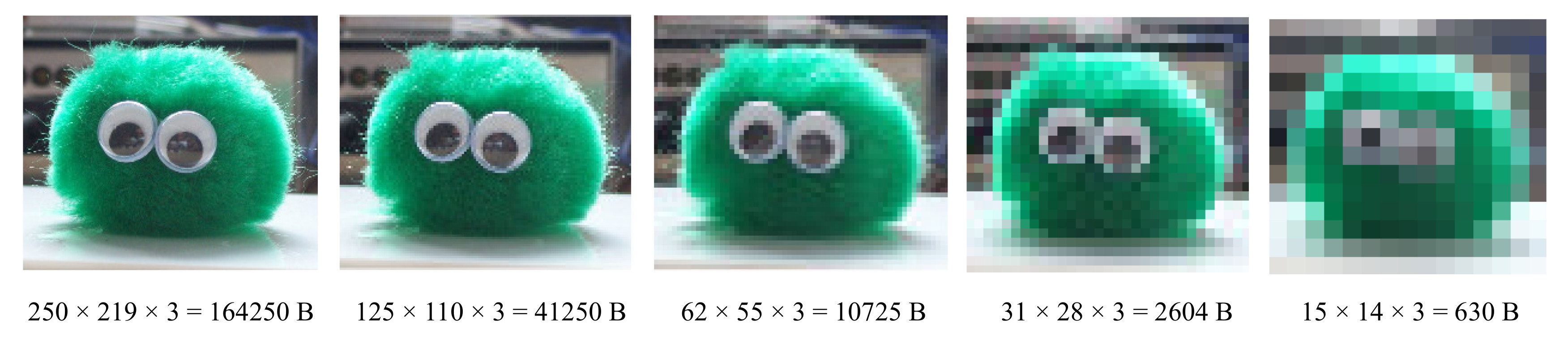
Figure 4 : Image resolution
As you can see if we were to use a 250 x 219 pixel image, which in the land of images is extremely small, we would need to increase the computer's memory size by a factor of 20-ish. Therefore, in the test cases we will be processing, images will tend towards the "lower" end of the resolution spectrum e.g. 30 x 30 pixels. This does still allow you to see a simple images, but more importantly for labs work these smaller images reduces simulation times i.e. processing less data, helping reduce debugging times etc. Note, remember the simpleCPU is a von Neumann architecture so we do also need some space to store program code, variables etc.
For these initial test cases the image data will be stored on the host PC and then loaded into the VHDL memory model used by the simpleCPU so that it can be processed. Therefore, the next problems to be solved are : How do we store images on the PC, and how do we store images in memory?
The image file format selected to store images on the PC is the Portable PixMap (PPM) image format, originally designed to send images within plain text emails. An example 3 x 3 pixel image using this format is shown in figure 5. The reason for selecting this format is that pixel data can be stored using a simple text format i.e. ASCII characters, and can therefore, be editted/viewed using a text editor e.g. Notepad. Storing data in this format is not very efficient from a file size point of view i.e. would take less space if a binary format was used, or data compression techniques were used. However, as the images are only 30 x 30 pixels, this inefficiency is not a significant disadvantage.
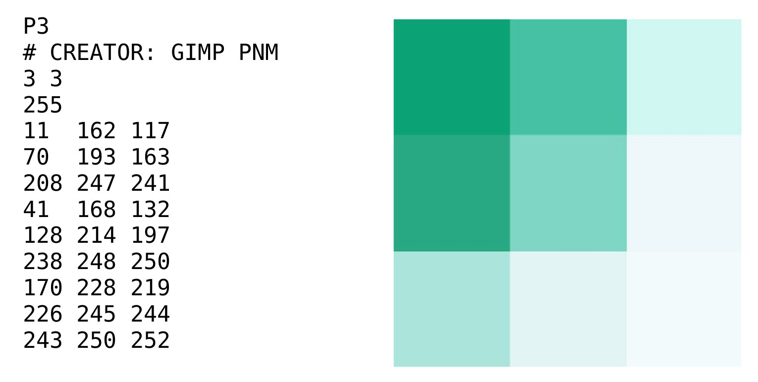
Figure 5 : PPM imge file (left), displayed image (right)
The first line of the PPM image file identifies the image format to the viewer by its "magic" number P3. This is then followed by a comment/description of the file, indicated by the leading # symbol. The next line defines the image size: columns (width) and rows (height). Lastly, the maximum value of each pixel (255). The remainder of the file defines the RGB value of each pixel, starting at the top left position within the image, a row at a time. Note, these RGB values are listed sequentially in the file, they do not need to be on the same line.
When interpreting RGB values i.e. what colour it represents, it is the relative size of each term, rather than their absolute values that counts e.g. the last pixel in the above image has a very large G term (250), from this you could assume that it would be green, however, as the the R & B terms are of a similar level it actually looks white. For a pixel to appear green the R & B terms will need to be smaller than the G term e.g. the first pixel in the image where G=162, R=11 and B=117, giving a green/blue colour.
The PPM image is automatically loaded into memory using the VHDL memory model ram_4Kx16_sim_v1a.vhd (Link). As the simpleCPU's memory can only store 16bit values, the 24bit RGB data has to be reduced in size, as shown in figure 6. The lower three bits of the RED and BLUE pixel values, and the lower two bits of the GREEN pixel value are removed, to produce a 16bit packed data type. This is done automatically by the VHDL memory component when the PPM image is loaded at the start of each simulation i.e. each pixel within the image is loaded into a separate memory location.
Note, the reason why the GREEN pixel data is 6-bits, rather than 5-bits used for the RED and BLUE values, is that the human eye is more sensitive to the GREEN component of light, therefore, we can detect a wider range of colours in this part of the spectrum, therefore, more bits.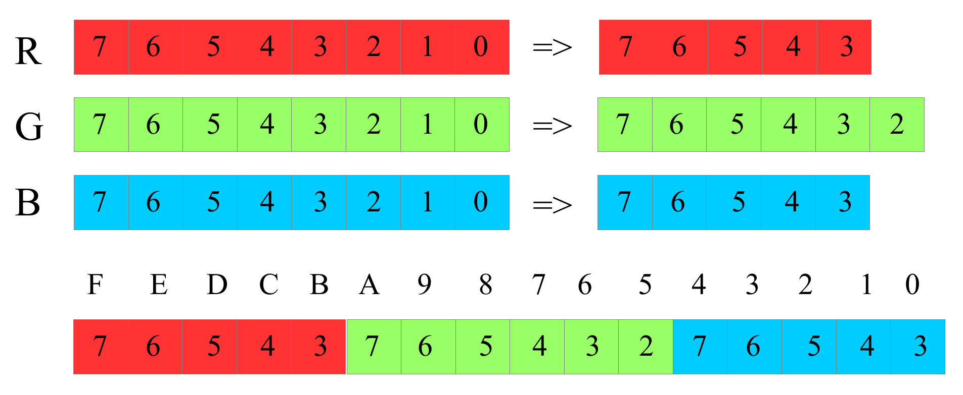
Figure 6 : packed RGB data format
To process this RGB packets data the simpleCPU processor will need to extract the original R, G and B values, then left shift these to regenerate the original 8-bit values, as shown in figure 7. Note, the lower bits will of these values will be lost but should not significantly affect the displayed colour.
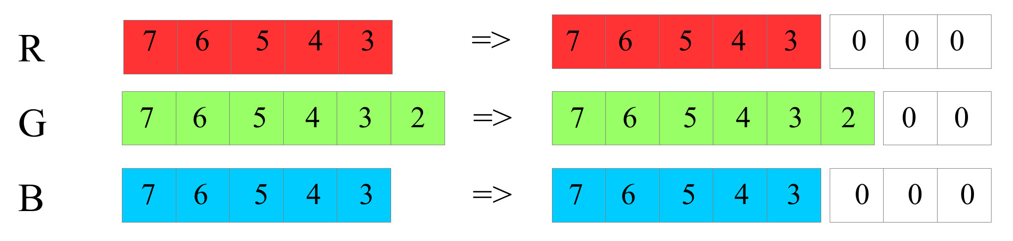
Figure 7 : packed RGB data format
To understand the types of operations that the processor needs to perform i.e. the required instruction set architecture, consider how you would convert the colour image shown in figure 5 into a grayscale image (Link), replacing each pixel's RGB value with its equivalent brightness. In the land of image processing the "brightness" (Y) can mean different things e.g. mean brightness, perceived brightness, luminance etc. Two commonly used equations used to calculate "brightness" (Y) from RGB values are:
Y = (R + G + B) / 3
Y = 0.33 R + 0.5 G + 0.16 B
The current instruction set does not support multiplication or division instructions, this is for a couple of reasons. Firstly the algorithms used to implement these functions are typically performed over a number of steps (Link)(Link) i.e. clock cycles. Therefore, the simpleCPU's execute phase would need to be modified as shown in figure 8. In this example the multiple (MUL) instruction needs 8 clock cycles to complete i.e. assumes that the algorithm used has 8 steps. This would require modifications to the processor's control logic e.g. replacing the 3 stage ring counter with a loadable 11 stage ring counter. This move to a variable execution length is possible, but less efficient from a hardware point of view i.e. this new control hardware is only used by one instruction. The second reason for not supporting these instructions is the size of the hardware used to implement these functions e.g. an n-bit array multiplier will have n-1 adders. That's a lot of hardware, increasing costs, but can also increase the critical path delay (CPD) i.e. the time it takes for a signal to pass through these logic gates and reach a final stable value. Therefore, we may need to increase the clock period, reducing the system's clock speed i.e. allow extra time for these more complex circuits to process their data. This is significant, as this effectively reduces the performance of the other instructions used in a program e.g. the ADD instruction will require less time to process its data, but as the clock speed is fixed it has to wait. Therefore, when assessing system performance we need to consider if its better to implement the algorithms in software running on simple hardware running at a higher clock speed, or on a system with more specialised hardware running at a slightly slower clock speed. The answer to this question normally boils down to how often an algorithm uses this specialised hardware e.g. digital filters use a lot of multiply and accumulate (MAC) instructions, so these would favour systems with hardware support.
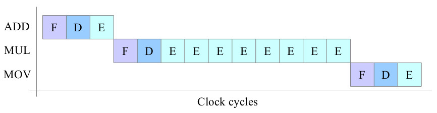
Figure 8 : possible multiply instruction timing
The second brightness equation (above) may look a bit more of an issue as we are dealing with fractional values, however, again with a little bit of sideways thinking we can get an approximate solution. Multiplication can be implemented using repeated addition e.g. R+R+R = 3 x R. For small values this isn't a big overhead, however, for larger values e.g. 1000 x R, it starts to become impractical. Division can be implemented using shift right instructions, each shift to the right divides by 2. Therefore, the second equation can be rewritten as:
Y = (0.375 R)    + (0.5 G)   + (0.125 B)
Y = (3/8 x R)    + (1/2 x G) + (1/8 x B)
Y = (R+R+R)>>3   + (G)>>1    + (B)>>3
Y = (R+R+R+B)>>3 + (G)>>1
Note "X >> N" reads as variable X is shifted right N bit positions. As we are limited by a fixed divide by 2, we can not get exactly the same weighting e.g. 0.375 rather than 0.33, however, for some algorithms this is close enough. Remember, fixed shifts to the left or right costs no hardware, we just need to rewire the connecting buses.
To prototype this algorithm i implemented a simple solution in python: (Link). The main loops are shown in figure 9, the input image is on the left and the resulting output image on the right.
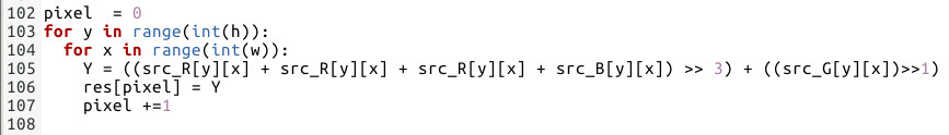


Figure 9 : Grayscale conversion
The image pixel values are contained in three, two dimensional arrays: src_R[][], src_G[][] and src_B[][], their resulting brightness value is stored in array res[]. This value is then written to the output file, being used as the new R,G and B value i.e. when R, G and B are equal the colour displayed is a shade of grey (brightness), ranging from 0,0,0=Black to 255,255,255=White.
To allow the simpleCPU processor to process the pixel data stored in memory it will need to regenerate the original RGB values from the packed data packet i.e. we will need to shift these bit values to the left. Therefore, to implement this operation we will need a shift instruction.
Note, we could implement the shift to the left via multiplication, using repeated addition, and shift to the right via division, using repeated subtraction, but this would incur a significant processing overhead. Also, as the brightness calculation will be shifting this data to the right anyway this cancels out some of these shifts.
Another point to consider is how a program accesses this data. In the original simpleCPU_v1a the ALU data width and MEM address width were both 8bits, therefore we could hardcode data (KK) or an address (AA) within an instruction i.e. immediate or absolute addressing modes, as shown in figure 10.
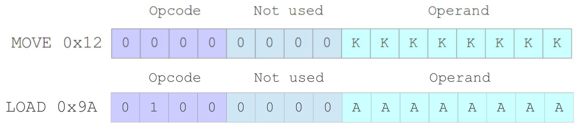
Figure 10 : SimpleCPU_v1a instruction formats
Working with the same fixed length 16-bit instruction format the simpleCPU_v1d runs into some problems i.e. we are now using 16-bit data and 12-bit addresses, but the instruction bit fields are the same size, as shown in figure 11. To get around this issue the LOAD instruction sacrifices flexibility to free up space within the instruction, allowing an 12-bit address to be defined i.e. the destination register for LOAD and STORE is hardcoded to register RA, you can not use RB,RC or RD. However, this technique will not work for the MOVE instruction i.e. how do we load a 16-bit data value into a register, as this would require a 24 bit instruction (8bit opcode + 16bit operand)?
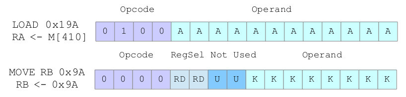
Figure 11 : SimpleCPU_v1d instruction formats
For small values e.g. signed 8-bit values, +127 to -128, we can get around this problem by automatically generating the high bits i.e. replicating the sign bit, as shown in figure 12. However, for larger values we still have a problem :(.
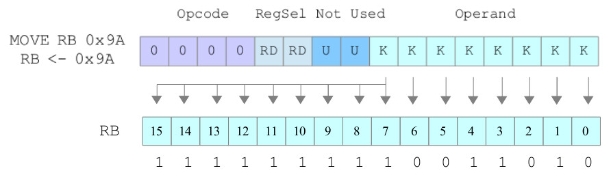
Figure 12 : sign extension
This may seem like a fundamental limitation, and from one point of view it is. This issue is common for most fixed length instruction format machines i.e. computers in which all instructions are the same length. To highlight this consider the MIPS processor (Link), your classic RISC processor. To simplify the instruction fetch and decode phases it uses a fixed length 32-bit instruction format, as shown in figure 13, supporting three basic types of instructions: register (R), immediate (I) and jump (J). Therefore, as each instruction is limited to 32-bits you can only define a 16bit immediate or a 26bit address, so it also runs into the same problems as it uses 32bit registers and a 32bit address bus.
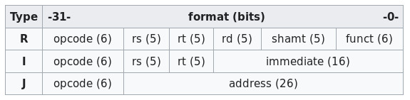
Figure 13 : MIPS instruction formats
To overcomes this problem the approach taken by most RISC type machines is rather than trying to define a single instruction that can load a register with a 32-bit value they make the assumption that most of the time we will be using smaller values, therefore, for the majority of the time these instructions will work just fine. For the odd occasion where we do need to specify larger values we can use multiple simple instructions to achieve the same result i.e. load a 32-bit value as two 16-bit chunks. For the MIPS :
"The Load Immediate Upper instruction copies the 16-bit immediate into the high-order 16 bits of a general purpose register (GPR). It is used in conjunction with the OR Immediate instruction to load a 32-bit immediate into a register."
The alternative solution is to move to a variable length instruction format. Here instructions can be defined over multiple memory locations, depending on the size of the data types used by its operands. To highlight this consider the 68000 family of processors (Link), your classic CISC processor. This processor again uses 32-bit data registers and a 32-bit address, however, a small twist to reduce costs the original design only had a 16-bit external data bus (more pins= more money). Now, if an instruction needs to use the absolute addressing mode i.e. define a 32-bit address, this instruction (bit-fields) can be stored in three memory locations. The first memory location defines the instruction's opcode, registers used and other parameters, the next two "extension" memory locations store the 32-bit address, as shown in figure 14. This address is automatically read into the processor as two 16-bit chunks to form the complete 32-bit address (16 bit memory locations). Moving to a variable length instruction format remove the limitations on what data types an instruction can use, increasing flexibility. The down side is that is adds complexity to the fetch phase e.g. what do we increment the PC to, what address is the next instruction stored in? Again, we run into the same issues as the previous multiply example, we can add addition hardware to overcome these issues, but if this is only used by a small number of instructions, hardware efficiency is reduced and costs increased.
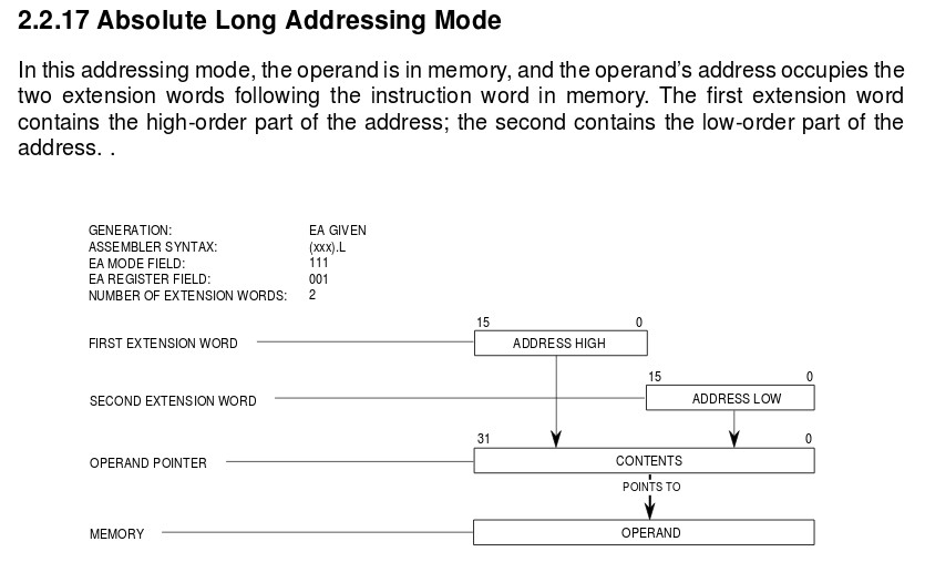
Figure 14 : variable length instruction formats
For the simpleCPU we are going to take the RISC approach and use multiple simple instruction to solve our problem, but rather than define a new type of MOVE instruction to load the high 8bits into a register, we will reuse the rotate instruction that we already need to implement.
To allow the simpleCPU to process the packed RGB image data ive added two new instructions to the simpleCPU_v1d's instruction set:
You may of noticed the lack of shift right instructions needed to implement the divide functions used in the brightness calculations. Decided to implement this function using the existing rotate left instruction i.e. one shift to the right is the same as fifteen shifts to the left, not very efficient but it saves adding new hardware to the ALU. The ASL can be implemented with a small modification to the rotate left (ROL) hardware block, as shown in figure 15. Now, rather than setting the LSB to the MSB it is simply set to 0 by ANDing it with the control signal CTL. The bitwise OR uses the same basic configuration as the existing bitwise AND, as shown in figure 16. The new instruction formats are shown in figure 17.
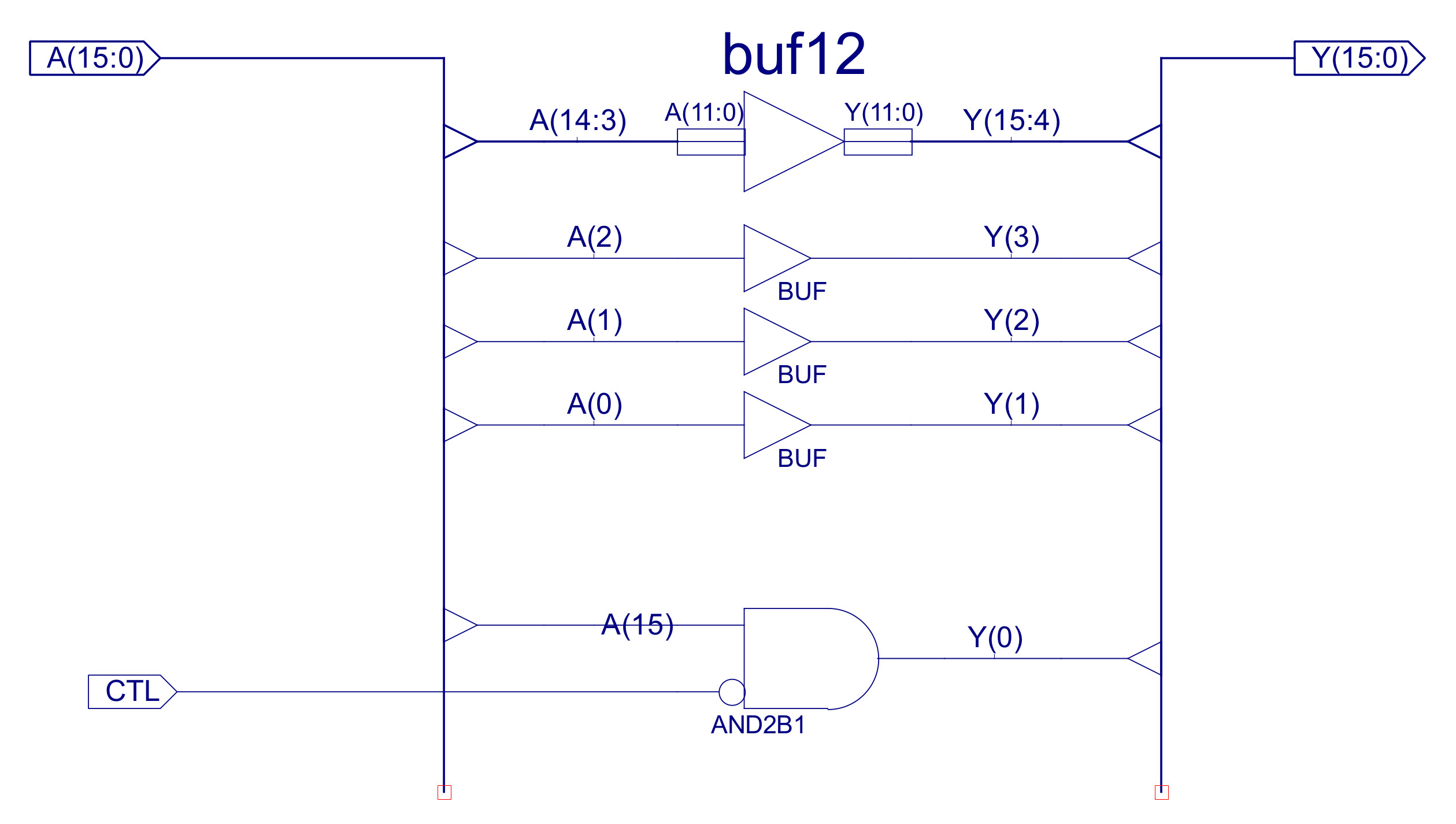
Figure 15 : variable length instruction formats
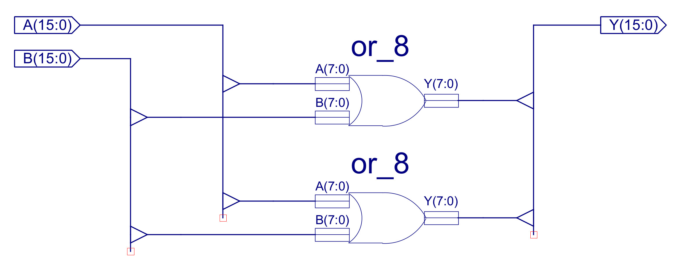
Figure 16 : variable length instruction formats

Figure 17 : ASL and OR instruction formats
Using these new instructions we can now load a 12-bit value (an address) into a register e.g. to load the value 703 into register RA :
move RA 32
asl RA
asl RA
asl RA
asl RA
or RA 191
To simplify coding these instructions can be replaced with the movea macro (move address):
#usage
movea( RA, address )

#simpleCPUv1d_p1.m4
define( movea, `AOP1( $1, $2 )
 AOP2( $1 )
 AOP2( $1 )
 AOP2( $1 )
 AOP2( $1 )
 AOP3( $1, $2 )')

#simpleCPUv1d_p2.m4
define( AOP1,`move $1 eval( ($2 & 0xF00) >> 4)' )
define( AOP2,`asl $1' )
define( AOP3,`or $1 eval( $2 & 0xFF)' )
However, a small complication is that the macro needs the address of the symbolic label i.e. the value 703. This is generated during the first pass of the assembler. Fortunately the two pass assembler can be manual configured to perform either the first or second pass. The updated batch file to run the assembler is shown in figure 18.
m4 simpleCPUv1d_p1.m4 $1 > code.asm
simpleCPUv1d_as.py -i code -p 1

m4 simpleCPUv1d_p2.m4 tmp.asm > code.asm
simpleCPUv1d_as.py -i code -o code -p 2

simpleCPUv1d_ld.py -i code
Figure 18 : new batch file go.bat (go.sh)
Note, in a two pass assembler, Pass-1 generates the symbol table i.e. calculates the address of each instruction and data values, allowing symbolic labels to be converted into actual addresses. Pass-2 then converts instruction mnemonics i.e. opcodes and operands, into machine code, generating the final machine code.
Again, to simplify coding the rotate functions can be replaced with the rotate_right and rotate_left macros:
#usage
rotate_right( RA, data )

#simpleCPUv1d_p1.m4
define( rotate_right, `
ifelse(eval($2==1), 1, `
  rol $1
  rol $1
  rol $1
  rol $1
  rol $1
  rol $1
  rol $1
  rol $1
  rol $1
  rol $1
  rol $1
  rol $1
  rol $1
  rol $1
  rol $1',)

...

ifelse(eval($2==12), 1, `
  rol $1
  rol $1
  rol $1
  rol $1',)
ifelse(eval($2==13), 1, `
  rol $1
  rol $1
  rol $1',)
ifelse(eval($2==14), 1, `
  rol $1
  rol $1',)
ifelse(eval($2==15), 1, `
  rol $1',)

#simpleCPUv1d_p1.m4
define( rotate_left, `
ifelse(eval($2==15), 1, `
  rol $1
  rol $1
  rol $1
  rol $1
  rol $1
  rol $1
  rol $1
  rol $1
  rol $1
  rol $1
  rol $1
  rol $1
  rol $1
  rol $1
  rol $1',)

...

ifelse(eval($2==4), 1, `
  rol $1
  rol $1
  rol $1
  rol $1',)
ifelse(eval($2==3), 1, `
  rol $1
  rol $1
  rol $1',)
ifelse(eval($2==2), 1, `
  rol $1
  rol $1',)
ifelse(eval($2==1), 1, `
  rol $1',)
')
This is implemented with a simple if-then-else tree, should of implemented using a loop, but went for the cut-and-paste solution :). Note, missed out some of the branches e.g. 2 - 11 for rotate right to save space, but you get the idea. The complete macro file can be downloaded with the assembler using the link at the top.
The final software element needed is s divide macro/subroutine i.e. needed for the calculation (R+G+B)/3. There are a range of divide algorithms that could be used, but to keep things simple i'm just going to use one based on repeated subtraction, as shown in figure 19.
#usage A=B/C
div( A, B, C )

#simpleCPUv1d_p2.m4
define( divide, `
  move RA 0
  store RA div_tmp
div_loop:
  load RA $2
  sub RA $3
  store RA $2
  rol RA
  and RA 0x01
  jumpnz div_exit
  load RA div_tmp
  add RA 1
  store RA div_tmp
  jump div_loop
div_exit:
  load RA $2
  add RA $3
  store RA $2
  load RA div_tmp
  store RA $1
div_tmp:
  .data 0'
)
Figure 19 : divide macro
Using these macros we can now implement a the grayscale code on the simpleCPU, as shown below:
start:
  movea( RC, 0x584 )
  movea( RD, 0x200 )

loop:
  load RA (RD)
  rotate_left( RA, 3 )
  and RA 0xF8
  store RA acc

  load RA (RD)
  rotate_right( RA, 3)
  and RA 0xFC
  addm RA acc
  store RA acc

  load RA (RD)
  rotate_right( RA, 8)
  and RA 0xF8
  addm RA acc
  store RA acc

  add RD 1

  divide( brightness, acc, 3 )

  load RA brightness
  rotate_right( RA, 3)
  and RA 0x1F
  store RA acc

  load RA brightness
  and RA 0xFC
  rotate_left( RA, 3)
  addm RA acc
  store RA acc

  load RA brightness
  and RA 0xF8
  rotate_left( RA, 8 )
  addm RA acc

  store RA (RC)
  add RC 1

  move RA RC
  subm RA end
  jumpz trap
  jump loop

trap:
  move RA 0
  store RA 0xFFF
  jump trap

brightness:
  .data 0
acc:
  .data 0
end:
  .data 0x908
In this example the image is loaded into memory using the packed RGB data type shown in figure 6, with a base address of 0x200, finishing at address 0x583. The resulting grayscale image is stored in memory at address 0x584, finishing at address 0x907. This information is passed to the VHDL memory model using its generic parameters, as shown in figure 20. The instruction memory region is also initialised using the file: code.dat, generated by the assembler from the above assembly code. The input image file: bug30x30.ppm must be stored in the top level project directory. The output image file: output.ppm is written to this directory when the memory's DUMP pin is pulsed. This pin has been memory mapped to address 0xFFF and is pulsed by the program when it enters the trap loop at the end of the program.
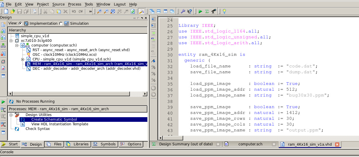
Figure 20 : ram_4Kx16_sim configuration parameters
The input and resulting output images are shown in figure 21. Running at 10MHz this takes the simple CPU approximately 365 ms to complete. Tip debugging your code can be tricky, to help in this process a simple VHDL based disassembler has been added to the test bench so that you can see what instructions are being executed. Another complexity when working at this level is how to figure out where you are in the program's execution. Typically this is done in high level programs by printing to the screen "got here" messages. The equivalent technique at this level is to use the test pin "TP". This output is memory mapped to address 0xFFE. Therefore, when you need to identify if a section of code has been executed you can execute the instruction STORE RA, 0xFFE and look for the TP pin to pulse high in the waveform diagram. Finally, start small. For initial testing use the 3x3 image in figure 5 as you input image, as simulations always take longer than you would like :).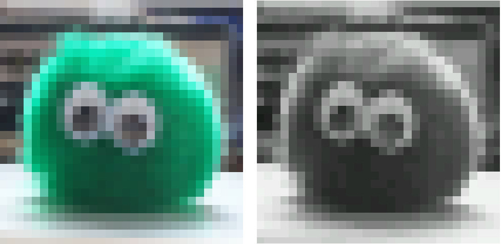
Figure 21 : input (left) and output (right) images
WORK IN PROGRESS

This work is licensed under a Creative Commons Attribution-NonCommercial-NoDerivatives 4.0 International License.
Contact email: mike@simplecpudesign.com