Figure 1 : simpleCPU with interrupts
Adding interrupts
Multiple sequential interrupts
Multiple parallel interrupts sources
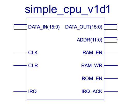
The continued development of the SimpleCPU, the version 1d1 :). This is your basic simpleCPU_v1d with a few extra ALU control lines to allow some flexibility in the instruction-set + interrupt support. Most people encounter interrupts when considering IO, however, i would argue that this is only one side of the coin. Interrupts are an architectural modification / improvement, not just an new type of "input". To place this discussion in context we need to define what an interrupt is, to me an interrupt is basically a hardware triggered subroutine call i.e. rather than the program using a CALL instruction to trigger the execution of a block of code, this "subroutine" is triggered by hardware within the processor. One of the first examples of interrupts being using in a computer is back in 1951 with UNIVAC (Link). This computer used interrupts to handle arithmetic overflows:
"The computer reacts to an "overflow" situation automatically. The sequence of instructions is interrupted, and the pair of instructions in memory location 000 is inserted. This insertion is effected after both instructions of the original pair have been executed even though overflow may have been caused by the first instruction of the pair."Not the easiest quotes (Link) to read, but if i'm reading this correctly, if an overflow occurred the main program's execution would be paused and two new instructions executed to handle this event, then normal execution is resumed. The key point to note here is that the main program is unaffected by the interrupt i.e. in terms of its execution. The main program is automatically paused to allow additional functionality to be performed that will handle this event, before its continues its execution. Note, these instructions do change the state of the program i.e. resulting from the overflow, but these actions are transparent to the main program. These types of internal events or "traps" are similar to the external interrupt requests we see when looking at IO. Again, the first examples of IO based interrupts date back to the later 1950's and were used to help reduce processing overheads associated with reading or writing data e.g. rather than a program having to wait for input data, an interrupt can be generated when it is available, allowing the computer to continue processing other tasks. One of the first examples of IO interrupts being using in a computer is back in 1956 with DYSEAC (Link) :
"The DYSEAC computer ... introduced the idea of input-output devices communicating directly with memory while a program is running, then interrupting the program upon completion."Again reading the original quotes (Link) are slightly confusing, but basically this computer supported Direct Memory Access (DMA) (Link), allowing IO devices to write their data directly to memory i.e. these transfers are not under the control of the processor. When complete these IO devices generate an interrupt, causing the main program to be suspended, allowing additional functionality to be performed to process this data. When complete the main program was again resumed. This type of external IO based interrupts are triggered using an Interrupt Request (IRQ) pin, an external "interface" pin e.g. consider a UART (serial port). When data is received by the UART it sets the interrupt pin on the processor, triggering the execution of the code associated with processing this input data, rather than the main program having to specifically read (poll) the UART's status register to see if data is available. The block of code used to handle this interrupt is typically called the Interrupt Service Routine (ISR).
Therefore, the architectural modifications needed within the processor to process internal or external events (interrupts) are:
A key point to remember is that to the main program an ISR is transparent i.e. the execution of this additional program should not corrupt the main program's state: flags, registers etc.
From the above list we can see that a new instruction is required: RTI. This is very similar to the existing RET instruction used to return control back to the main program from a subroutine CALL, however, this new instruction also restores the processor's hardware state that was automatically check-pointed (in hardware) when the interrupt was performed. Other considerations not highlighted in this list are how an interrupt is signalled and if an interrupt can be interrupted?
Typically, external IO interrupts are viewed as either level or edge sensitive, as shown in figure 2.
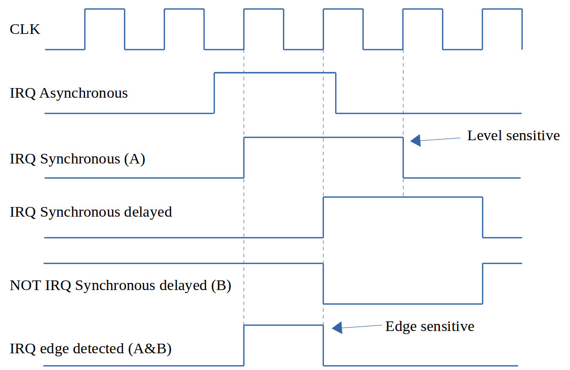
Figure 2 : interrupt signal
External signals to the processor will not necessarily be synchronised to the system clock i.e. they can change at any time, therefore, the first step for any IRQ representation is to synchronise this signal to the system clock by passing it through a D-type flip-flop. If the interrupt is level sensitive i.e. active when this signal is a logic '1', the signal "IRQ synchronised" in figure 2 is used to trigger the interrupt process. Therefore, the duration of this signal needs to be long enough to be detected by the processor. Depending when this signal is sampled within the simpleCPU it could take 3 clock cycles to process i.e. the time it takes to execute an instruction. In the example shown in figure 2 the "IRQ synchronised" signal is only 2 clock cycles long, therefore, it may be missed if this signal is only sampled/tested at the end of each instruction. Alternatively, an interrupt may edge sensitive. Rather than the value/level of the signal being significant, its the transition from a 0 to a 1 that triggers the interrupt. To detect this transition the inverted version of the delayed "IRQ synchronised" can be ANDed with the original version using the circuit shown in figure 3.
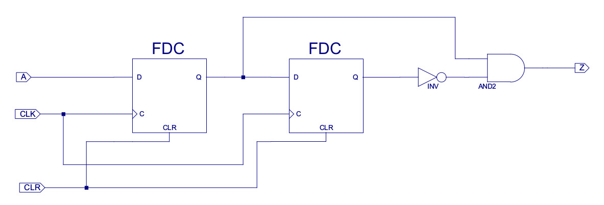
Figure 3 : edge detector
Using the D-type flip-flop outputs from these two flip-flops the logic AND of the inverted old (default/initial) logic 0 and the new (interrupt) logic 1 is performed i.e. this output will only go to a logic 1 on the initial edge. When the D-type flip-flops both contain 0s or 1s the output will be a logic 0. Again, this pulse may be missed by the processor e.g. if it is in the middle of processing a main program instruction. Therefore, these signals can be passed into a SR flip-flop i.e. used to drive the SET input, implementing an interrupt flag. Note, SR flip-flops can be implemented in a number of different ways e.g. using the classic crossed couple NOR/NAND gates, or a synchronous version shown in figure 4, in the simpleCPU this circuit is used to implement the interrupt-triggered flag and the interrupt-active flag.
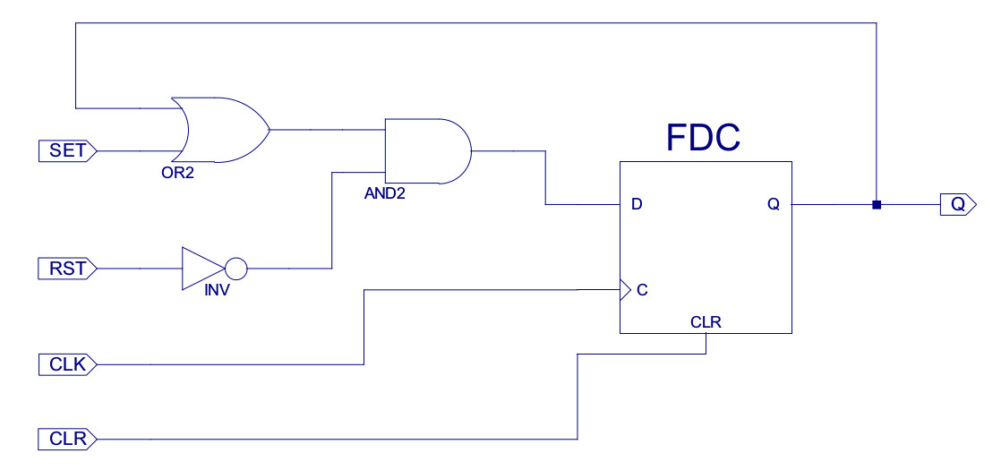
Figure 4 : synchronous SR flip-flop
The next new hardware component needed to implement interrupts on the simpleCPU is the hardware needed to checkpoint the processor's state i.e. the status register. A simple method commonly used to implement this functionality are shadow registers i.e. a replicated status register. When an interrupt occurs rather than making a copy of this register's data, the main program's status register is disabled i.e. locked, and the interrupt's shadow status register is switched in. The circuit used to implement this is shown in figure 5.
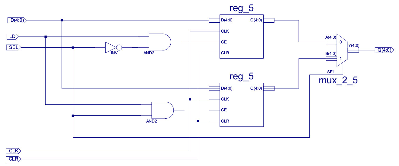
Figure 5 : shadow register file
Another key step in the implementation of an interrupt is the saving and updating of the program counter (PC). This can be implemented using the existing PC component with a couple of small modifications. For this simpleCPU the address of the ISR will be fixed. For some processors this is hard-coded into the processor e.g. for the first version of the Xilinx PicoBlaze processor this address (vector) was fixed to address 0xFF. However, to allow a little more flexibility this address or Interrupt Vector (shown in figure 6) is defined as a constant within the PC and selected using a multiplexer (MUX_3_12). This value can be altered to match the software implementation used e.g. for the initial test program this was set to the value 0x009. As with the existing CALL/RET instructions the return address used after the interrupt is finished is store on the LIFO stack, however, as the PC has already been incremented when this value is pushed onto the stack (as part of the previous instruction's FDE), the CIN input and the MUX_3_12 select line are controlled by a new control line PC_ISR, selecting the Interrupt Vector as the next PC value and disabling the increment function when the return address is pushed onto the stack.
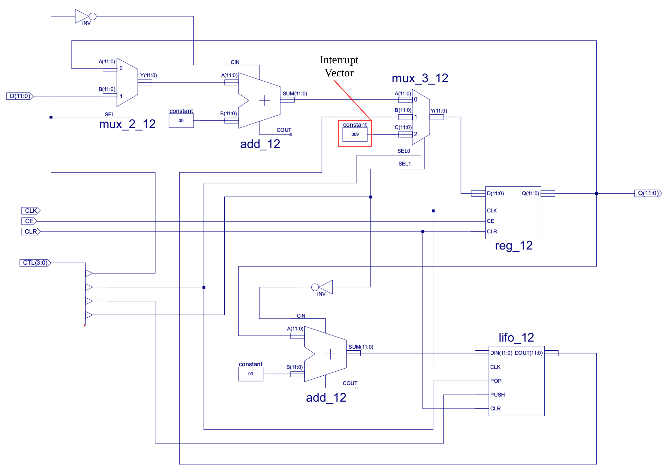
Figure 6 : program counter modifications
To restore the check-pointed processor state and to pop off the return address a new instruction is defined: Return from Interrupt (RTI) as shown in figure 7.
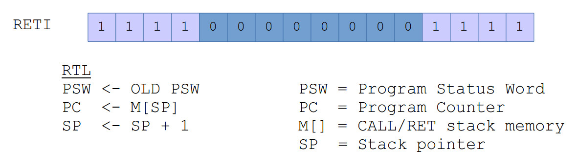
Figure 7 : return from interrupt instruction
This instruction is basically the same as the RET instruction, but it also clears the interrupt-triggered and interrupt-active flags. The final element needed to implement interrupts on the simpleCPU is to update the decode logic as shown in figure 8.
library IEEE;
use IEEE.STD_LOGIC_1164.ALL;

entity decoder is
Port (
   fetch          : in  STD_LOGIC;
   decode         : in  STD_LOGIC;
   execute        : in  STD_LOGIC;

   state          : in  STD_LOGIC_VECTOR(4 DOWNTO 0);
   reg_sel         : in  STD_LOGIC_VECTOR(3 DOWNTO 0);

   move           : in  STD_LOGIC;
   add            : in  STD_LOGIC;
   sub            : in  STD_LOGIC;
   bitWiseAnd     : in  STD_LOGIC;

   load           : in  STD_LOGIC;
   store          : in  STD_LOGIC;
   addm           : in  STD_LOGIC;
   subm           : in  STD_LOGIC;

   jumpu          : in  STD_LOGIC;
   jumpz          : in  STD_LOGIC;
   jumpnz         : in  STD_LOGIC;
   jumpc          : in  STD_LOGIC;
   call           : in  STD_LOGIC;

   type_d         : in  STD_LOGIC;
   type_e         : in  STD_LOGIC;
   type_f         : in  STD_LOGIC;

   y0             : in  STD_LOGIC;
   y1             : in  STD_LOGIC;
   y2             : in  STD_LOGIC;
   y3             : in  STD_LOGIC;
   y4             : in  STD_LOGIC;
   y5             : in  STD_LOGIC;
   y6             : in  STD_LOGIC;
   y7             : in  STD_LOGIC;
   y8             : in  STD_LOGIC;
   y9             : in  STD_LOGIC;
   yA             : in  STD_LOGIC;
   yB             : in  STD_LOGIC;
   yC             : in  STD_LOGIC;
   yD             : in  STD_LOGIC;
   yE             : in  STD_LOGIC;
   yF             : in  STD_LOGIC;

   irq_trig        : in  STD_LOGIC;
   irq_active      : in  STD_LOGIC;
   irq_set         : out STD_LOGIC;
   irq_rst         : out STD_LOGIC;

   ir_en          : out STD_LOGIC;

   pc_en          : out STD_LOGIC;
   pc_ld          : out STD_LOGIC;
   pc_push        : out STD_LOGIC;
   pc_pop         : out STD_LOGIC;
   pc_irq         : out STD_LOGIC;

   reg_X1         : out STD_LOGIC;
   reg_X0         : out STD_LOGIC;
   reg_Y1         : out STD_LOGIC;
   reg_Y0         : out STD_LOGIC;
   reg_en         : out STD_LOGIC;

   alu_ctl4       : out STD_LOGIC;
   alu_ctl3       : out STD_LOGIC;
   alu_ctl2       : out STD_LOGIC;
   alu_ctl1       : out STD_LOGIC;
   alu_ctl0       : out STD_LOGIC;

   addr_sel1      : out STD_LOGIC;
   addr_sel0      : out STD_LOGIC;

   data_sel2      : out STD_LOGIC;
   data_sel1      : out STD_LOGIC;
   data_sel0      : out STD_LOGIC;

   ram_en         : out STD_LOGIC;
   ram_wr         : out STD_LOGIC;
   rom_en         : out STD_LOGIC;

   update_state   : out STD_LOGIC;
   sel_state      : out STD_LOGIC );

end decoder;

architecture decoder_arch of decoder is

   signal zero           : STD_LOGIC;
   signal carry          : STD_LOGIC;
   signal overflow       : STD_LOGIC;
   signal pos            : STD_LOGIC;
   signal neg            : STD_LOGIC;

   signal jump           : STD_LOGIC;
   signal write_mem      : STD_LOGIC;
   signal irq_enable     : STD_LOGIC;
   signal irq_disable    : STD_LOGIC;

   signal ret            : STD_LOGIC;
   signal move_reg       : STD_LOGIC;
   signal load_indirect  : STD_LOGIC;
   signal store_indirect : STD_LOGIC;

   signal rotate_left    : STD_LOGIC;
   signal xor_reg        : STD_LOGIC;

   signal reti           : STD_LOGIC;

begin

   -- map state input bus to status bits

   zero     <= state(0);
   carry    <= state(1);
   overflow <= state(2);
   pos      <= state(3);
   neg      <= state(4);

   -- generate zero operand / register / indirect instruction ctl lines

   ret            <= type_f and y0;
   move_reg       <= type_f and y1;
   load_indirect  <= type_f and y2;
   store_indirect <= type_f and y3;

   rotate_left    <= type_f and y4;
   xor_reg        <= type_f and yA;

   reti           <= type_f and yF;

   -- interal logic

   jump           <= ( jumpu or (jumpz and zero) or (jumpnz and not zero) or (jumpc and neg) or call or ret );

   write_mem      <= store or store_indirect;

   irq_enable     <= (execute and (not jump) and irq_trig and (not irq_active));
   irq_disable    <= reti;

   -- external logic

   ir_en          <= fetch;

   pc_en          <= (decode and (not jump)) or (execute and jump) or (irq_enable) or (execute and irq_disable) ;
   pc_ld          <= (execute and jump) or (irq_enable) or (execute and irq_disable);

   pc_push        <= (decode and call) or (irq_enable);
   pc_pop         <= (execute and ret) or (execute and irq_disable);

   pc_irq         <= (irq_enable);

   reg_X1         <= (reg_sel(3) and not(load or store or addm or subm));
   reg_X0         <= (reg_sel(2) and not(load or store or addm or subm));

   reg_Y1         <= reg_sel(1);
   reg_Y0         <= reg_sel(0);

   reg_en         <= (execute and (move or load or add or sub or bitWiseAND or
                                   addm or subm or
                                   move_reg or load_indirect or
                                   rotate_left or xor_reg )) ;

   -- CTL4  CTL3 CTL2 CTL1 CTL0
   -- X     0    0    0    0     ADD
   -- X	    0    0    0    1     SUB
   -- X	    0    0    1    0     BITWISE AND / XOR
   -- X	    0    0    1    1     -
   -- X	    0    1    0    0     PASS B
   -- X	    0    1    0    1     -
   -- X	    0    1    1    0     ROTATE LEFT
   -- X	    0    1    1    1     -
   -- X	    1    0    0    0
   -- X	    1    0    0    1
   -- X	    1    0    1    0
   -- X	    1    0    1    1
   -- X	    1    1    0    0
   -- X	    1    1    0    1
   -- X	    1    1    1    0
   -- X	    1    1    1    1

   alu_ctl4       <= '0';
   alu_ctl3       <= '0';
   alu_ctl2       <= move or load or move_reg or load_indirect or rotate_left;
   alu_ctl1       <= bitWiseAND or rotate_left or xor_reg;
   alu_ctl0       <= sub or subm or xor_reg;

   -- SEL1 SEL0
   -- 0    0    PC
   -- 0    1    IR
   -- 1    0    REG
   -- 1    1    NU

   addr_sel1      <= (decode or execute) and (load_indirect or store_indirect);
   addr_sel0      <= (decode or execute) and (load or store or addm or subm);

   -- SEL2 SEL1 SEL0
   --  0   0    0     IR 8bit unsigned
   --  1   0    0     IR 8bit sign extended
   --  X   0    1     IR 12bit unsigned
   --  X   1    0     DATA-BUS-IN 16bit
   --  X   1    1     RY 16bit

   data_sel2      <= not(bitWiseAND);
   data_sel1      <= load or addm or subm or load_indirect or move_reg or xor_reg;
   data_sel0      <= move_reg or xor_reg;

   ram_en         <= (decode or execute) and (load or store or addm or subm or load_indirect or store_indirect);
   ram_wr         <= execute and (store or store_indirect);
   rom_en         <= fetch;

   update_state   <= (execute and (add or sub or bitWiseAND or addm or subm or rotate_left or xor_reg));
   sel_state      <= irq_active;

   irq_set        <= irq_enable;
   irq_rst        <= reti;

end decoder_arch;
Figure 8 : decode logic
When designing this logic i decided to not allow CALL and RET instructions to be interrupted, to simplify this further i decided to make this all JUMP instructions. I may have been over thinking this, but i thought there may be some issues in pushing / popping two addresses onto or off the stack at the same time e.g. interrupting a CALL/RET instruction. This means that there are two interrupt flags: interrupt-triggered and interrupt-active. If an interrupt occurs during one of these instructions the interrupt will not be performed, but the interrupt-triggered flag is set so that the processor knows an interrupt request has occurred. When the main program reaches an instruction that can be interrupted the interrupt is performed and the interrupt-active flag is set. The final updated decode logic schematic is shown in figure 9.
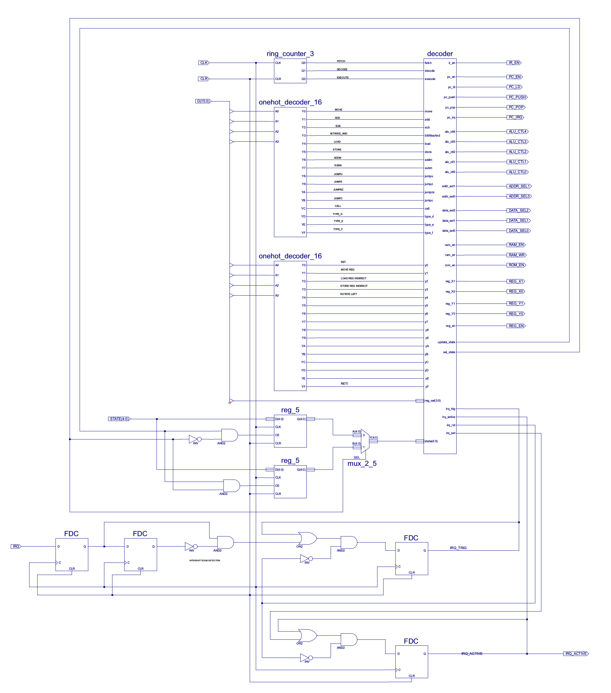
Figure 9 : decode logic schematic
To test the operation of the interrupt the following test program was used:
start:
    move ra 1
    move ra 2
    move ra 3
    move ra 4
    move ra 5
    move ra 6
    move ra 7
    move ra 8
    jump start

isr:
    call checkpoint
    move ra 9
    add ra 1
    call restore
    reti

checkpoint:
    store ra mem_ra
    move ra rb
    store ra mem_rb
    move ra rc
    store ra mem_rc
    move ra rd
    store ra mem_rd
    ret

restore:
    load ra mem_rd
    move rd ra
    load ra mem_rc
    move rc ra
    load ra mem_rb
    move ra rb
    load ra mem_ra
    ret

mem_ra:
    .data 0
mem_rb:
    .data 0
mem_rc:
    .data 0
mem_rd:
    .data 0
The address of the first instruction in the ISR is address 0x009, therefore, the constant in the PC component is set to this value. The main program repeatedly sets register RA to the values 1,2,3,4,5,6,7,8. On entry to the ISR the checkpoint subroutine is called this copies the values contained in registers RA,RB,RC and RD out to memory, so that they are free to be modified by the interrupt service routine. The ISR loads RA with the value 9 and adds 1. Note, changed these values later to set different status bits i.e. to check that the status register was working correctly. When complete the restore subroutine is called to restore the old values of registers RA,RB,RC and RD i.e. back to the values used in the main program, slight over kill as some of these registers were not changed, but went for a worst case / general case solution. Then finally the RETI instruction is performed to return back to the main program. The waveform simulation of this program + external interrupt is shown in figure 10.
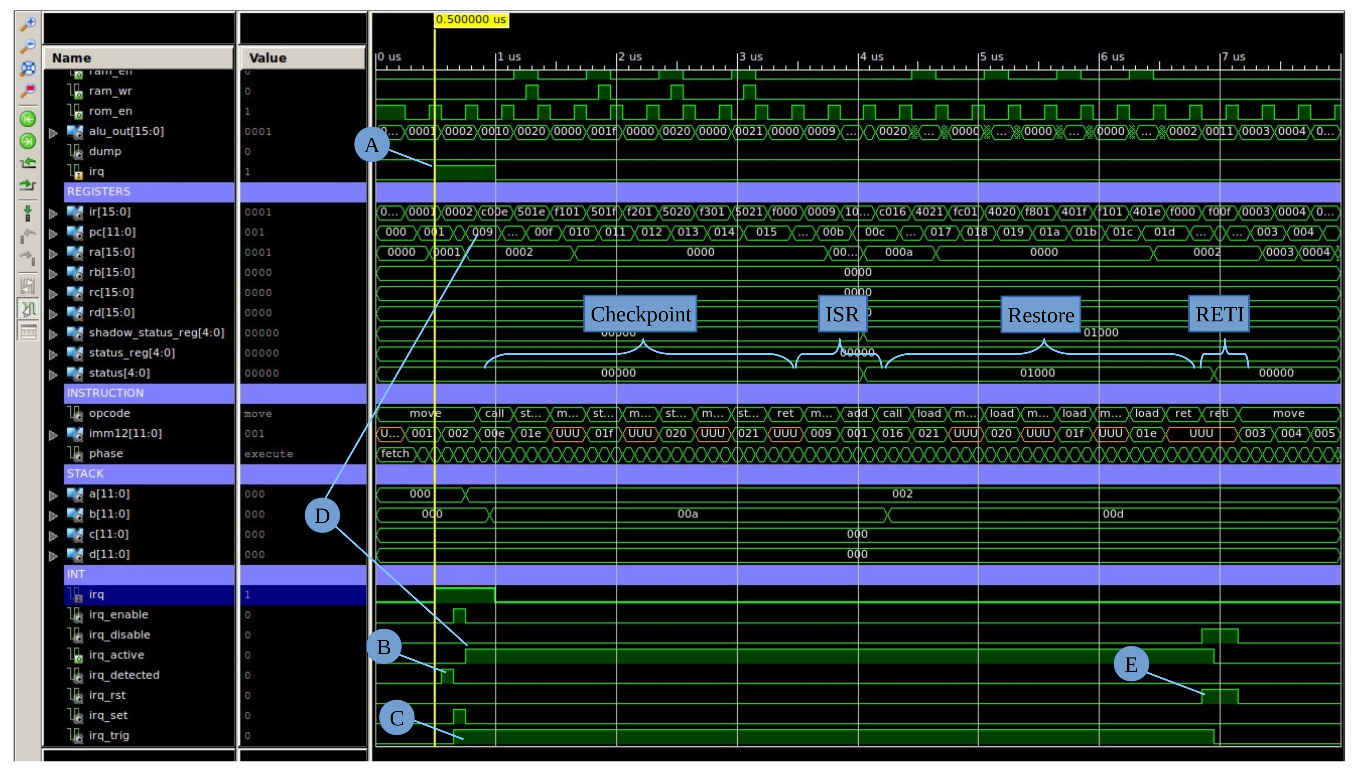
Figure 10 : interrupt simulation
To try and step through this waveform. At point "A" the IRQ line goes high. This is part way through a clock cycle, therefore, it is not detected in hardware until point "B" i.e. when it is registered in a D-type flip-flop and the rising edge is detected. This signal is then used to set the interrupt-triggered flag at point "C". When the current main program instruction is completed the processor will perform the interrupt (point D), pushing the current PC value onto the stack and jumping to the interrupt vector i.e. address 0x009, the first address of the ISR. The checkpoint subroutine is then performed, then the ISR's function, then the restore subroutine and finally the RETI at point "E". The interrupt is then complete, the return address is popped off the stack and the main program continues its execution i.e. the interrupt occurred as the value 2 was stored in RA, therefore, the next value stored in RA is 3, then 4 ...
The ISE project and assembler used in this simulation is available here: (Link), (Link)
To show interrupts in context consider the schematic shown in figure 11. This system has an 8bit input port and an 8bit output port. Connected to the input port are eight switches and to the output port eight LEDs. Without interrupts the processor would need to explicitly read the input port to see if a button is being pressed, then update its associated LED. However, using interrupts we can move this functionality into the interrupt service routine. Assuming each switch outputs a logic 1 when pressed we can logically OR these signals together using the OR_8 component, such that when any switch is pressed the processor's interrupt pin is set high, triggering the ISR. Note, we still need to test each input port bit to see what switch is pressed, however, this functionality is only called when it is needed, rather than the main program having to explicitly test each input port bit to see if it have been pressed.
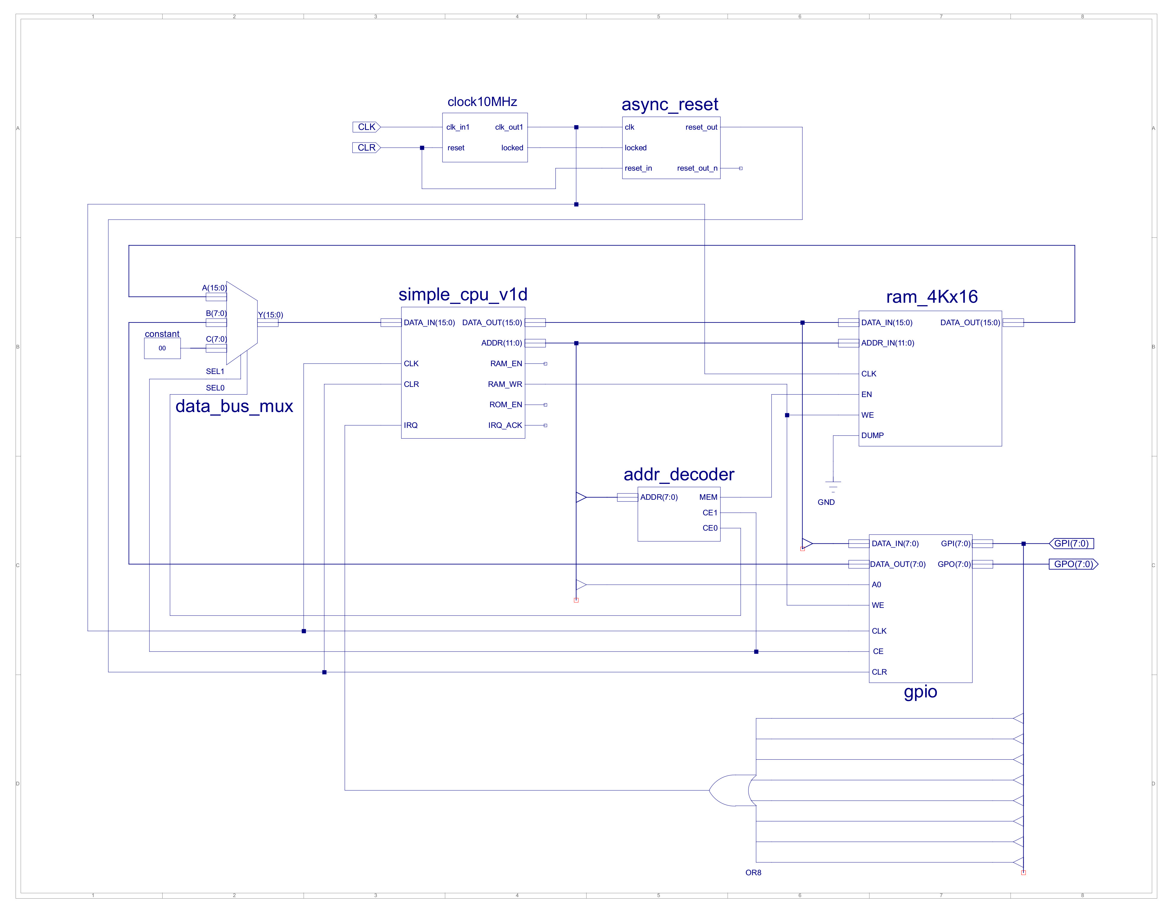
Figure 11 : interrupts using switches
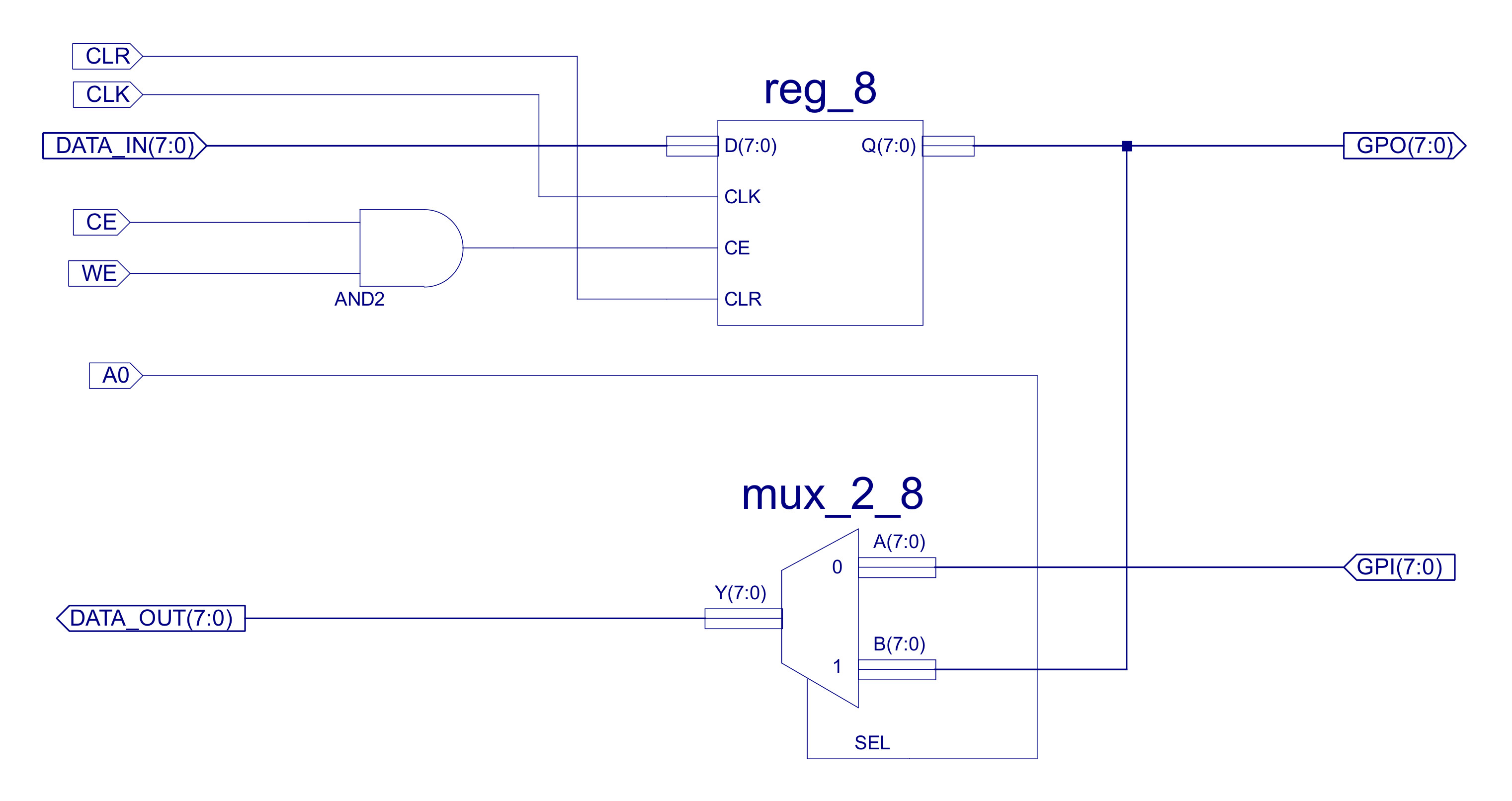
Figure 12 : GPIO port hardware
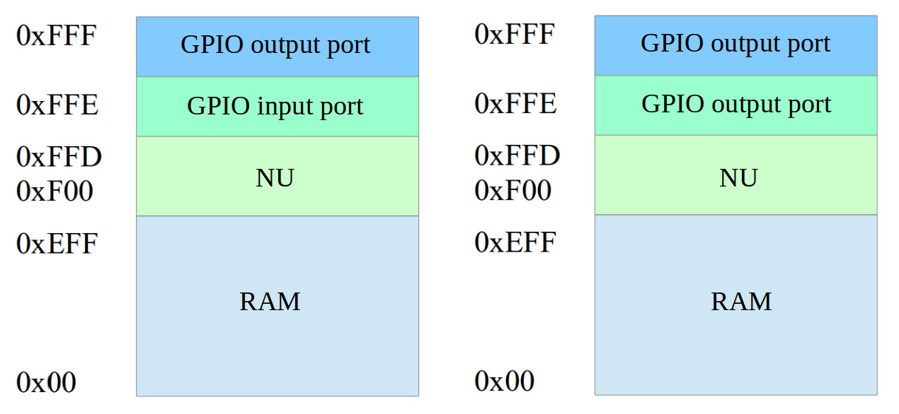
Figure 13 : GPIO memory map
Without interrupts we would need to Poll the input port i.e. repeatedly read address 0xFFE as shown in the program below. The program initially reads the input port, performs a bitwise AND to see if any of the bits are non-zero i.e. a button is pressed. If there are, it then tests each bit to see which button is pressed, generating the correct output LED bit value in register RB, before writing this to the output port. At first consideration this program may seem quite inefficient i.e. repeatedly checking to see if the switches connected to the input port have been pressed, however, if the processor has nothing else to do, this solution is as good as any, as we shall see when we consider the one based on interrupts
start:
    load ra 0xFFE
    and ra 0xFF
    jumpz start
    called update
    jump start

update:
    move ra 0
    move rb 0
    store ra 0xFFF

bit1:
    load ra 0xFFE
    and ra 1
    jumpz test bit2
    add rb 1

bit2:
    load ra 0xFFE
    and ra 2
    jumpz test bit4
    add rb 2

bit4:
    load ra 0xFFE
    and ra 4
    jumpz test bit8
    add rb 4

bit8:
    load ra 0xFFE
    and ra 8
    jumpz test bit16
    add rb 8

bit16:
    load ra 0xFFE
    and ra 16
    jumpz test bit32
    add rb 16

bit32:
    load ra 0xFFE
    and ra 32
    jumpz test bit64
    add rb 32

bit64:
    load ra 0xFFE
    and ra 64
    jumpz test bit128
    add rb 64

bit128:
    load ra 0xFFE
    and ra 128
    jumpz test finish
    add rb 128

finish:
    move ra rb
    and ra 0xFF
    store ra 0xFFF
    ret
In this example code we will use the eight input OR gate to trigger the processor's interrupt, as shown in the program below. The Interrupt Vector within the PC would be set to address 0x001 i.e. the address of the CALL checkpoint instruction. The main program is an infinite loop which "waits" for an interrupt. When an interrupt occurs the processor will jump to the ISR and call the same update subroutine. Note, the MOVE instruction in the main program loop is only there as the jump instruction is not interruptable :).
start:
    move ra 0
    jump start

isr:
    call checkpoint
    call update
    call restore
    reti

update:
    move ra 0
    move rb 0
    store ra 0xFFF

bit1:
    load ra 0xFFE
    and ra 1
    jumpz test bit2
    add rb 1

bit2:
    load ra 0xFFE
    and ra 2
    jumpz test bit4
    add rb 2

bit4:
    load ra 0xFFE
    and ra 4
    jumpz test bit8
    add rb 4

bit8:
    load ra 0xFFE
    and ra 8
    jumpz test bit16
    add rb 8

bit16:
    load ra 0xFFE
    and ra 16
    jumpz test bit32
    add rb 16

bit32:
    load ra 0xFFE
    and ra 32
    jumpz test bit64
    add rb 32

bit64:
    load ra 0xFFE
    and ra 64
    jumpz test bit128
    add rb 64

bit128:
    load ra 0xFFE
    and ra 128
    jumpz test finish
    add rb 128

finish:
    move ra rb
    and ra 0xFF
    store ra 0xFFF
    ret
As the previous examples shows interrupts are only really useful if the processor has something else that it needs to do i.e. multiple tasks sharing the processor's time. With this type of bare metal system if your program is not running there is nothing else for the system to do i.e. the main program is an infinite loop. Note, this also shows that there are significant overheads in using interrupts e.g. the checkpoint and restore subroutines. These could be skipped in this example as the main program does not have a state i.e. it does not matter if RA or RB are altered, however, in general you would need to use these subroutines, therefore, incur their processing delays. The question of whether to using interrupts or polling boils down to the time between samples i.e. how busy the processor is, how long does it take to perform its tasks and therefore, the time between it looking at (sampling) the input port, and how quickly the tasks associated with the interrupt need to be performed e.g. if the processor does not read a UART (serial port) quickly enough a received CHAR will be overwritten by the next received CHAR (if no hardware FIFO or buffering used).
Figure 14 shows the waveform simulation of the interrupt based solution on the OR gate based system shown in figure 11. In this simulation the GPI input is set to different values i.e. 1,2,4,8,16,32,64 and 128, simulating each switch being pressed in turn i.e. setting and clearing each bit. The input port values must be held for approximately 10us to ensure that the ISR has a chance to read the input port's value i.e. identify the button pressed. If the input port state is not held stable for this time the button state may be missed i.e. the switch must be held stable for the execution time of the ISR, otherwise the input port may have returned back to its default value before it is read i.e. the interrupt will be triggered but the wrong value read. Note, this interrupt based solution also finctions differently to the polling implementation in the event that switches are not released i.e. the OR gate's output will not return to zero, therefore, an interrupt will not be generated.
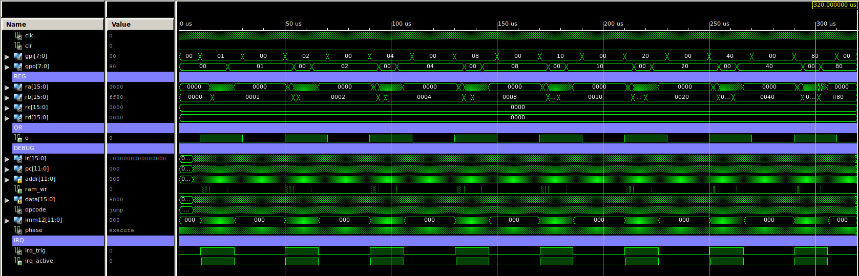
Figure 14 : GPIO OR gate based interrupt simulation
Hmmmm, an opps in the first design i did not consider what would happen when an interrupt occurs during an interrupt, not in terms of interrupting an interrupt, but rather recording that a second interrupt has occurred. Note, it would not be practical for the simpleCPU to support the interruption of interrupts i.e. starting a second instance of the ISR, as the return-address stack (LIFO) is only four elements deep. Therefore, multiple interrupts will soon burn through this stack making subroutines impossible, possibly crashing the main program. To allow a new interrupt to be registered during an interrupt only small modifications to the control logic are needed i.e. the control_logic.sch shown in figure 15 and decode.vhd, such that the interrupt_triggered and interrupt_active flags are updated correctly. The new and updated ISE project used in this simulation is available here: (Link).
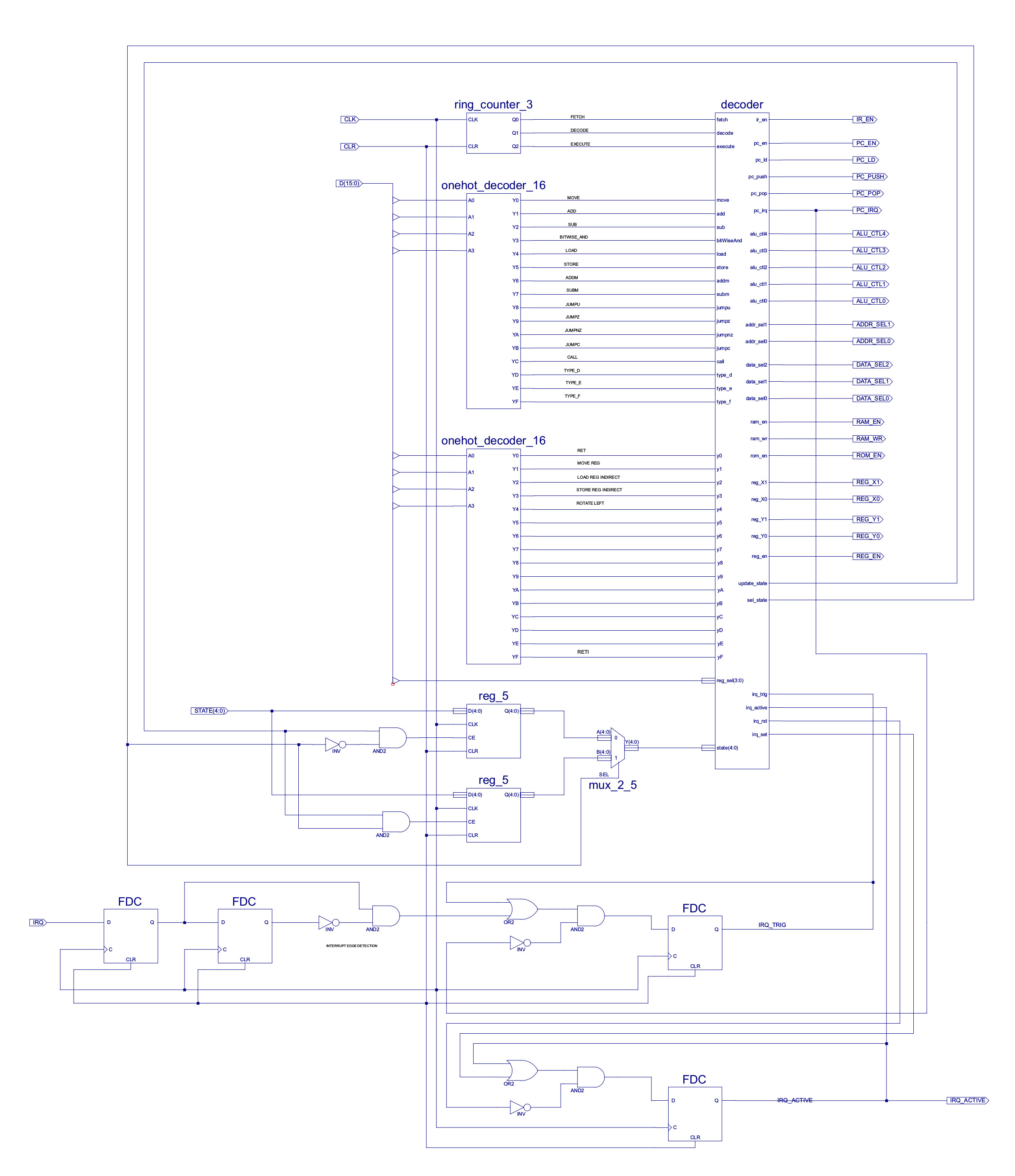
Figure 15 : modification to decode logic
To test this new design the original test code is modified with a second interrupt pulse i.e. an interrupt is generated when an interrupt is being processed, as shown in figure 16. The original interrupt is processed as normal, however the interrupt_triggered flag is now reset at the start of the interrupt service routine, so that it can be set by the second interrupt pulse. When the first interrupt is complete the RETI instruction is executed, returning control back to the main program. One main program instruction is then executed before the second interrupt is processed.
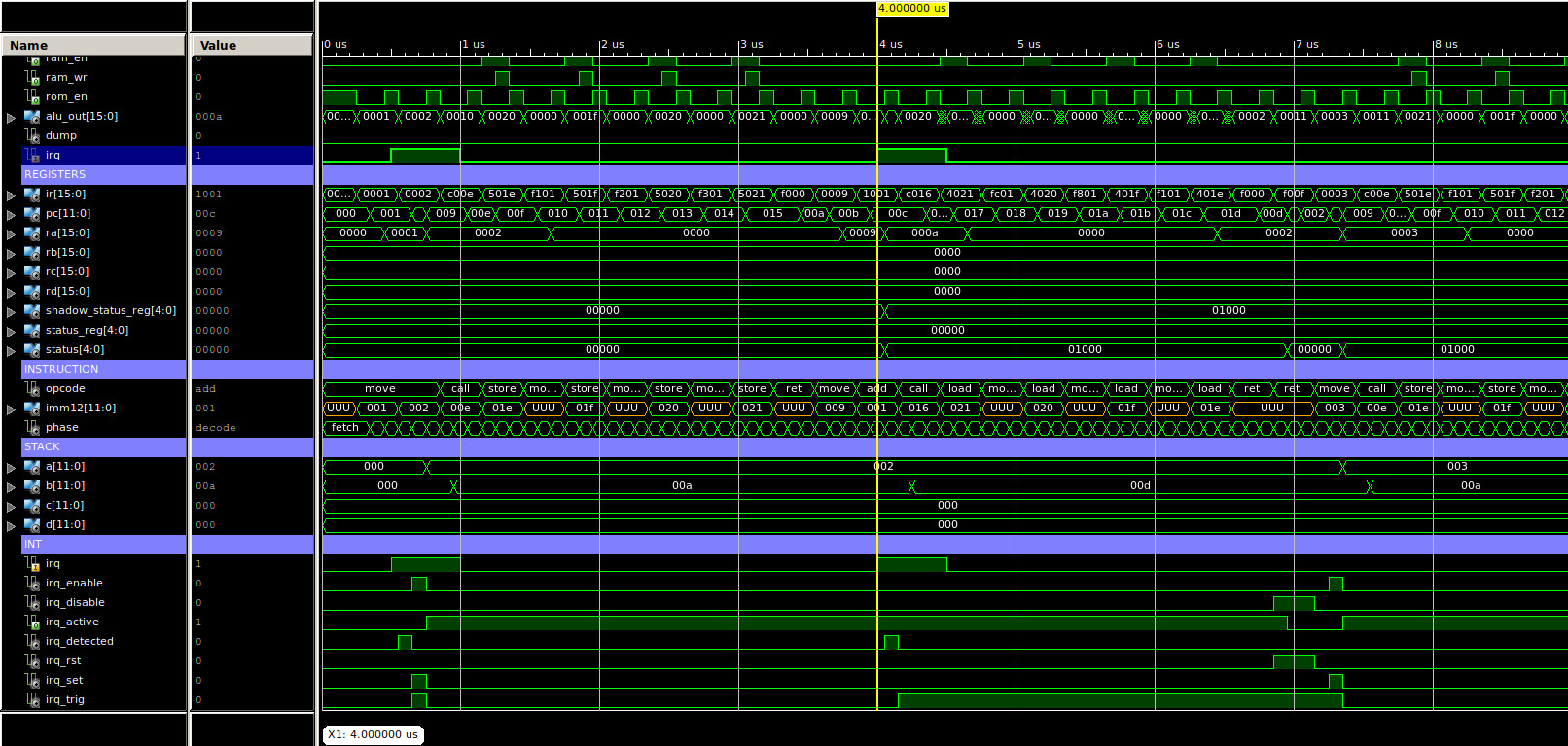
Figure 16 : multiple interrupt simulation
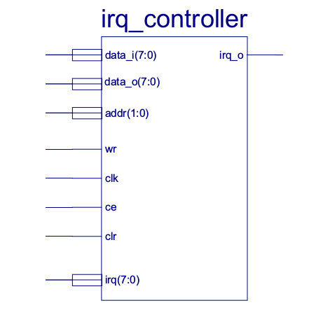
Figure 17 : simpleCPU interrupt controller
If a processor has one FDE engine there can only be one interrupt i.e. there is only one program to interrupt. However, typically we have multiple peripheral devices (GPIO, UART, TIMER, DMA etc) wanting to get the processor's attention i.e. we have multiple interrupt sources. A simple solution to this problem is to logically OR these signals together, however, in the case of multiple interrupts being generated at the same time, each peripheral device would need to maintain a status registers and detect if the processor had accessed this information i.e. when an interrupt is generated the processor would need to poll each of these status registers and peripheral devices would need to wait until its ISR had been processed. Therefore, to support multiple interrupts and simplify there implementation on the processor you typically use an interrupt controller i.e. a new hardware component, to record what interrupts have occurred, assign priorities to each of these interrupts and interrupt processor accordingly i.e. the interrupt controller is placed in between the peripheral devices and the processor. The hardware used by the interrupt controller can be defined using schematics, but to save time the simpleCPU's is written in VHDL as shown below:
-- =============================================================================================================
-- * File Name: simpleCPU_irq_controller.vhd
-- *
-- * Version: V1.0
-- *
-- * Release Date:
-- *
-- * Author(s): M.Freeman
-- *
-- * Description: A simple irq handler/controller
-- *
-- * Conditions of Use: THIS CODE IS COPYRIGHT AND IS SUPPLIED "AS IS" WITHOUT WARRANTY OF ANY KIND, INCLUDING,
-- *                    BUT NOT LIMITED TO, ANY IMPLIED WARRANTY OF MERCHANTABILITY AND FITNESS FOR A
-- *                    PARTICULAR PURPOSE.
-- *
-- * Notes:
-- *
-- =============================================================================================================

LIBRARY IEEE;
USE IEEE.STD_LOGIC_1164.ALL;
USE IEEE.STD_LOGIC_UNSIGNED.ALL;

LIBRARY UNISIM;
USE UNISIM.vcomponents.ALL;

ENTITY irq_controller IS
PORT (
  clk    : IN  STD_LOGIC;
  clr    : IN  STD_LOGIC;
  addr   : IN  STD_LOGIC_VECTOR(1 DOWNTO 0);
  data_i : IN  STD_LOGIC_VECTOR(7 DOWNTO 0);
  data_o : OUT STD_LOGIC_VECTOR(7 DOWNTO 0);
  ce     : IN  STD_LOGIC;
  wr     : IN  STD_LOGIC;
  irq    : IN  STD_LOGIC_VECTOR(7 DOWNTO 0);
  irq_o  : OUT STD_LOGIC );
END irq_controller;

ARCHITECTURE irq_controller_arch OF irq_controller IS

  --
  -- components
  --

  COMPONENT sr_ff
  PORT (
    clk   : IN STD_LOGIC;
    clr   : IN STD_LOGIC;
    set   : IN STD_LOGIC;
    reset : IN STD_LOGIC;
    d     : OUT STD_LOGIC );
  END COMPONENT;

  --
  -- signals
  --

  TYPE state IS ( S0, S1, S2, S3, S4, S5, S6, S7, S8, S9 );
  SIGNAL present_state, next_state : state;

  SIGNAL en : STD_LOGIC_VECTOR(1 DOWNTO 0);
  SIGNAL write : STD_LOGIC;
  SIGNAL read : STD_LOGIC;
  SIGNAL idle : STD_LOGIC;

  SIGNAL irq_0 : STD_LOGIC;
  SIGNAL irq_1 : STD_LOGIC;
  SIGNAL irq_2 : STD_LOGIC;
  SIGNAL irq_3 : STD_LOGIC;
  SIGNAL irq_4 : STD_LOGIC;
  SIGNAL irq_5 : STD_LOGIC;
  SIGNAL irq_6 : STD_LOGIC;
  SIGNAL irq_7 : STD_LOGIC;

  SIGNAL irq_0_rst : STD_LOGIC;
  SIGNAL irq_1_rst : STD_LOGIC;
  SIGNAL irq_2_rst : STD_LOGIC;
  SIGNAL irq_3_rst : STD_LOGIC;
  SIGNAL irq_4_rst : STD_LOGIC;
  SIGNAL irq_5_rst : STD_LOGIC;
  SIGNAL irq_6_rst : STD_LOGIC;
  SIGNAL irq_7_rst : STD_LOGIC;

  SIGNAL irq_0_rst_int : STD_LOGIC;
  SIGNAL irq_1_rst_int : STD_LOGIC;
  SIGNAL irq_2_rst_int : STD_LOGIC;
  SIGNAL irq_3_rst_int : STD_LOGIC;
  SIGNAL irq_4_rst_int : STD_LOGIC;
  SIGNAL irq_5_rst_int : STD_LOGIC;
  SIGNAL irq_6_rst_int : STD_LOGIC;
  SIGNAL irq_7_rst_int : STD_LOGIC;

  SIGNAL irq_0_flag : STD_LOGIC;
  SIGNAL irq_1_flag : STD_LOGIC;
  SIGNAL irq_2_flag : STD_LOGIC;
  SIGNAL irq_3_flag : STD_LOGIC;
  SIGNAL irq_4_flag : STD_LOGIC;
  SIGNAL irq_5_flag : STD_LOGIC;
  SIGNAL irq_6_flag : STD_LOGIC;
  SIGNAL irq_7_flag : STD_LOGIC;

  SIGNAL status : STD_LOGIC_VECTOR(7 DOWNTO 0);
  SIGNAL command : STD_LOGIC_VECTOR(7 DOWNTO 0);
  SIGNAL trigger : STD_LOGIC_VECTOR(7 DOWNTO 0);

BEGIN

  --
  -- signal buffers
  --

  idle <= not ce;

  status <= irq_7_flag & irq_6_flag & irq_5_flag & irq_4_flag &
            irq_3_flag & irq_2_flag & irq_1_flag & irq_0_flag;

  irq_0 <= irq(0);
  irq_1 <= irq(1);
  irq_2 <= irq(2);
  irq_3 <= irq(3);
  irq_4 <= irq(4);
  irq_5 <= irq(5);
  irq_6 <= irq(6);
  irq_7 <= irq(7);

  irq_0_rst <= en(1) or irq_0_rst_int;
  irq_1_rst <= en(1) or irq_1_rst_int;
  irq_2_rst <= en(1) or irq_2_rst_int;
  irq_3_rst <= en(1) or irq_3_rst_int;
  irq_4_rst <= en(1) or irq_4_rst_int;
  irq_5_rst <= en(1) or irq_5_rst_int;
  irq_6_rst <= en(1) or irq_6_rst_int;
  irq_7_rst <= en(1) or irq_7_rst_int;

  --
  -- processes
  --

  bus_ctl : PROCESS( clk, clr )
  BEGIN
    IF clr='1'
	 THEN
      write <= '0';
      read <= '0';
    ELSIF clk='1' and clk'event
    THEN
      write <= wr and ce;
      read <= (not wr) and ce;
    END IF;
  END PROCESS;

  -- 0xFFF = Irq handler : write command register / read command register
  -- 0xFFE = Irq handler : read trigger source (clears trigger source)
  -- 0xFFD = Irq handler : write clear global status / read global status

  input_data_decoder : PROCESS( addr, wr )
  BEGIN
    IF wr='1'
    THEN
      CASE addr IS
        WHEN "11" =>   en <= "01";  -- command reg
        WHEN "01" =>   en <= "10";  -- clear status
        WHEN OTHERS => en <= "00";  -- null
      END CASE;
    ELSE
      en <= "00";
    END IF;
  END PROCESS;

  --
  -- Address
  -- -------
  --
  -- 0xFFF = Irq handler : write command register / read command register
  -- 0xFFE = Irq handler : read trigger source (clears trigger source)
  -- 0xFFD = Irq handler : write clear global status / read global status
  --
  output_data_decoder : PROCESS( addr, command, trigger, status )
  BEGIN
    CASE addr IS
      WHEN "11" =>
        data_o <= command;
      WHEN "00" =>
        data_o <= trigger;
      WHEN "01" =>
        data_o <= status;
      WHEN OTHERS =>
        data_o <= (OTHERS=>'0');
    END CASE;
  END PROCESS;

  --
  -- command register
  --
  -- Bit 7 : irq_7 enable (1=enable, 0=disable)
  -- Bit 6 : irq_6 enable (1=enable, 0=disable)
  -- Bit 5 : irq_5 enable (1=enable, 0=disable)
  -- Bit 4 : irq_4 enable (1=enable, 0=disable)
  -- Bit 3 : irq_3 enable (1=enable, 0=disable)
  -- Bit 2 : irq_2 enable (1=enable, 0=disable)
  -- Bit 1 : irq_1 enable (1=enable, 0=disable)
  -- Bit 0 : irq_0 enable (1=enable, 0=disable)
  --
  command_register : PROCESS(clk, clr)
  BEGIN
    IF clr='1'
    THEN
      command <= "00000000";
    ELSIF clk='1' and clk'event
    THEN
      IF en(0)='1'
      THEN
        command <= data_i;
      END IF;
    END IF;
  END PROCESS;

  --
  -- components
  --

  irq_0_latch : sr_ff PORT MAP(
    clk => clk,
    clr => clr,
    set => irq_0,
    reset => irq_0_rst,
    d => irq_0_flag );

  irq_1_latch : sr_ff PORT MAP(
    clk => clk,
    clr => clr,
    set => irq_1,
    reset => irq_1_rst,
    d => irq_1_flag );

  irq_2_latch : sr_ff PORT MAP(
    clk => clk,
    clr => clr,
    set => irq_2,
    reset => irq_2_rst,
    d => irq_2_flag );

  irq_3_latch : sr_ff PORT MAP(
    clk => clk,
    clr => clr,
    set => irq_3,
    reset => irq_3_rst,
    d => irq_3_flag );

  irq_4_latch : sr_ff PORT MAP(
    clk => clk,
    clr => clr,
    set => irq_4,
    reset => irq_4_rst,
    d => irq_4_flag );

  irq_5_latch : sr_ff PORT MAP(
    clk => clk,
    clr => clr,
    set => irq_5,
    reset => irq_5_rst,
    d => irq_5_flag );

  irq_6_latch : sr_ff PORT MAP(
    clk => clk,
    clr => clr,
    set => irq_6,
    reset => irq_6_rst,
    d => irq_6_flag );

  irq_7_latch : sr_ff PORT MAP(
    clk => clk,
    clr => clr,
    set => irq_7,
    reset => irq_7_rst,
    d => irq_7_flag );

  --
  -- state machine
  --
  sync : PROCESS(clk, clr)
  BEGIN
    IF clr='1'
    THEN
      present_state <= S0;
    ELSIF clk'event and clk='1'
    THEN
      present_state <= next_state;
    END IF;
  END PROCESS;

  comb: PROCESS( present_state,
                 command, read, write, ce,
                 irq_0_flag, irq_1_flag, irq_2_flag, irq_3_flag,
                 irq_4_flag, irq_5_flag, irq_6_flag, irq_7_flag )

  BEGIN
    irq_0_rst_int <= '0';
    irq_1_rst_int <= '0';
    irq_2_rst_int <= '0';
    irq_3_rst_int <= '0';
    irq_4_rst_int <= '0';
    irq_5_rst_int <= '0';
    irq_6_rst_int <= '0';
    irq_7_rst_int <= '0';
    irq_o <= '0';
    trigger <= "00000000";

    CASE present_state IS

      WHEN S0 =>

        IF irq_0_flag='1' and command(0)='1'
        THEN
          next_state <= S1;
        ELSIF irq_1_flag='1' and command(1)='1'
        THEN
          next_state <= S2;
        ELSIF irq_2_flag='1' and command(2)='1'
        THEN
          next_state <= S3;
        ELSIF irq_3_flag='1' and command(3)='1'
        THEN
          next_state <= S4;
        ELSIF irq_4_flag='1' and command(4)='1'
        THEN
          next_state <= S5;
        ELSIF irq_5_flag='1' and command(5)='1'
        THEN
          next_state <= S6;
        ELSIF irq_6_flag='1' and command(6)='1'
        THEN
          next_state <= S7;
        ELSIF irq_7_flag='1' and command(7)='1'
        THEN
          next_state <= S8;
        ELSE
          next_state <= S0;
        END IF;

      WHEN S1 =>
        irq_o <= '1';
        trigger <= "00000001";

        IF read='1' and not ce='1'
        THEN
          irq_0_rst_int <= '1';
          next_state <= S9;
        ELSE
          next_state <= S1;
        END IF;

      WHEN S2 =>
        irq_o <= '1';
        trigger <= "00000010";

        IF read='1' and not ce='1'
        THEN
          irq_1_rst_int <= '1';
          next_state <= S9;
        ELSE
          next_state <= S2;
        END IF;

      WHEN S3 =>
        irq_o <= '1';
        trigger <= "00000100";

        IF read='1' and not ce='1'
        THEN
          irq_2_rst_int <= '1';
          next_state <= S9;
        ELSE
          next_state <= S3;
        END IF;

      WHEN S4 =>
        irq_o <= '1';
        trigger <= "00001000";

        IF read='1' and not ce='1'
        THEN
          irq_3_rst_int <= '1';
          next_state <= S9;
        ELSE
          next_state <= S4;
        END IF;

      WHEN S5 =>
        irq_o <= '1';
        trigger <= "00010000";

        IF read='1' and not ce='1'
        THEN
          irq_4_rst_int <= '1';
          next_state <= S9;
        ELSE
          next_state <= S5;
        END IF;

      WHEN S6 =>
        irq_o <= '1';
        trigger <= "00100000";

        IF read='1' and not ce='1'
        THEN
          irq_5_rst_int <= '1';
          next_state <= S9;
        ELSE
          next_state <= S6;
        END IF;

      WHEN S7 =>
        irq_o <= '1';
        trigger <= "01000000";

        IF read='1' and not ce='1'
        THEN
          irq_6_rst_int <= '1';
          next_state <= S9;
        ELSE
          next_state <= S7;
        END IF;

      WHEN S8 =>
        irq_o <= '1';
        trigger <= "10000000";

        IF read='1' and not ce='1'
        THEN
          irq_7_rst_int <= '1';
          next_state <= S9;
        ELSE
          next_state <= S8;
        END IF;

      WHEN S9 =>
        irq_o <= '0';
        next_state <= S0;

      WHEN OTHERS =>
        next_state <= S0;
    END CASE;
  END PROCESS;


END irq_controller_arch;
This interrupt controller has eight interrupts: irq_0, irq_1, irq_2, irq_3, irq_4, irq_5, irq_6 and irq_7, with irq_0 being the highest priority and irq_7 the lowest i.e. the order that interrupts with be handled if multiple interrupts occur at the same time. Note, if the highest priority interrupt is repeatedly re-triggered, the lower priority ISR will not be processed, also as in the previous system an interrupt can not be interrupted i.e. if a low priority interrupt is being processed it can not be interrupted by a high priority interrupt, an interrupt must be completed (RETI executed) before the interrupt_triggered flag is examined again. In the system using this interrupt controller its internal registers have been memory mapped to the top of memory:
ADDR         WRITE                           READ                REG
0xFFF   command register               command register          3
0xFFD   clear trigger source            global status            1
0xFFC   clear trigger source            trigger source           0
Each interrupt (irq_0-irq_7) can be individually enabled or disabled by writing the appropriate bit pattern to the command register e.g. writing the value 0x82 to this register (addr 0xFFF) will enable interrupts 7 and 1, disabling interrupts 0,2,3,4,5 and 6.
command register
----------------

Bit 7 : irq_7 enable (1=enable, 0=disable)
Bit 6 : irq_6 enable (1=enable, 0=disable)
Bit 5 : irq_5 enable (1=enable, 0=disable)
Bit 4 : irq_4 enable (1=enable, 0=disable)
Bit 3 : irq_3 enable (1=enable, 0=disable)
Bit 2 : irq_2 enable (1=enable, 0=disable)
Bit 1 : irq_1 enable (1=enable, 0=disable)
Bit 0 : irq_0 enable (1=enable, 0=disable)
When an interrupt occurs the processor can determine the interrupt source by reading the trigger source register (address 0xFFE), this will return the one-hot value of the highest priority interrupt source:
trigger source register
-----------------------

IRQ 0 : 00000001
IRQ 1 : 00000010
IRQ 2 : 00000100
IRQ 3 : 00001000
IRQ 4 : 00010000
IRQ 5 : 00100000
IRQ 6 : 01000000
IRQ 7 : 10000000
Note, if two interrupt occur at the same time only the highest IRQ is shown (the lowest IRQ value). If this register is then re-read the next highest IRQ source is returned. Alternatively the processor can read the global status register, this returns the status of all interrupt flags on the interrupt controller, 0=false, 1=true:
global source register
----------------------

Bit :  76543210
IRQ 7 -||||||||
IRQ 6 --|||||||
IRQ 5 ---||||||
IRQ 4 ----|||||
IRQ 3 -----||||
IRQ 2 ------|||
IRQ 1 -------||
IRQ 0 --------|
Writing or reading to either of these registers will reset the current active interrupt flag. In the event that multiple interrupts having occurred at the same time, or different interrupts have occurred during an interrupt, these events are logged in the interrupt controller i.e. each interrupt has its own interrupt flag. Therefore, when the global or trigger source registers are read/written from/to the controller resets the highest priority flag, updating these registers and if required generating a new interrupt pulse on the processor's interrupt pin. Note, this controller will not log/process multiple interrupt pulses from the same interrupt pin i.e. if multiple interrupt pulses occur on interrupt 0 before its ISR has started only one interrupt will be processed. However, as soon as the global or trigger source registers are accessed that interrupt flag is re-enabled, such that if this interrupt was generated again during its ISR it would be the next interrupt processed.
To show this hardware in action consider the system shown in figure 18. This system has an GPIO port, an UART and a TIMER peripheral device i.e. three interrupt sources.
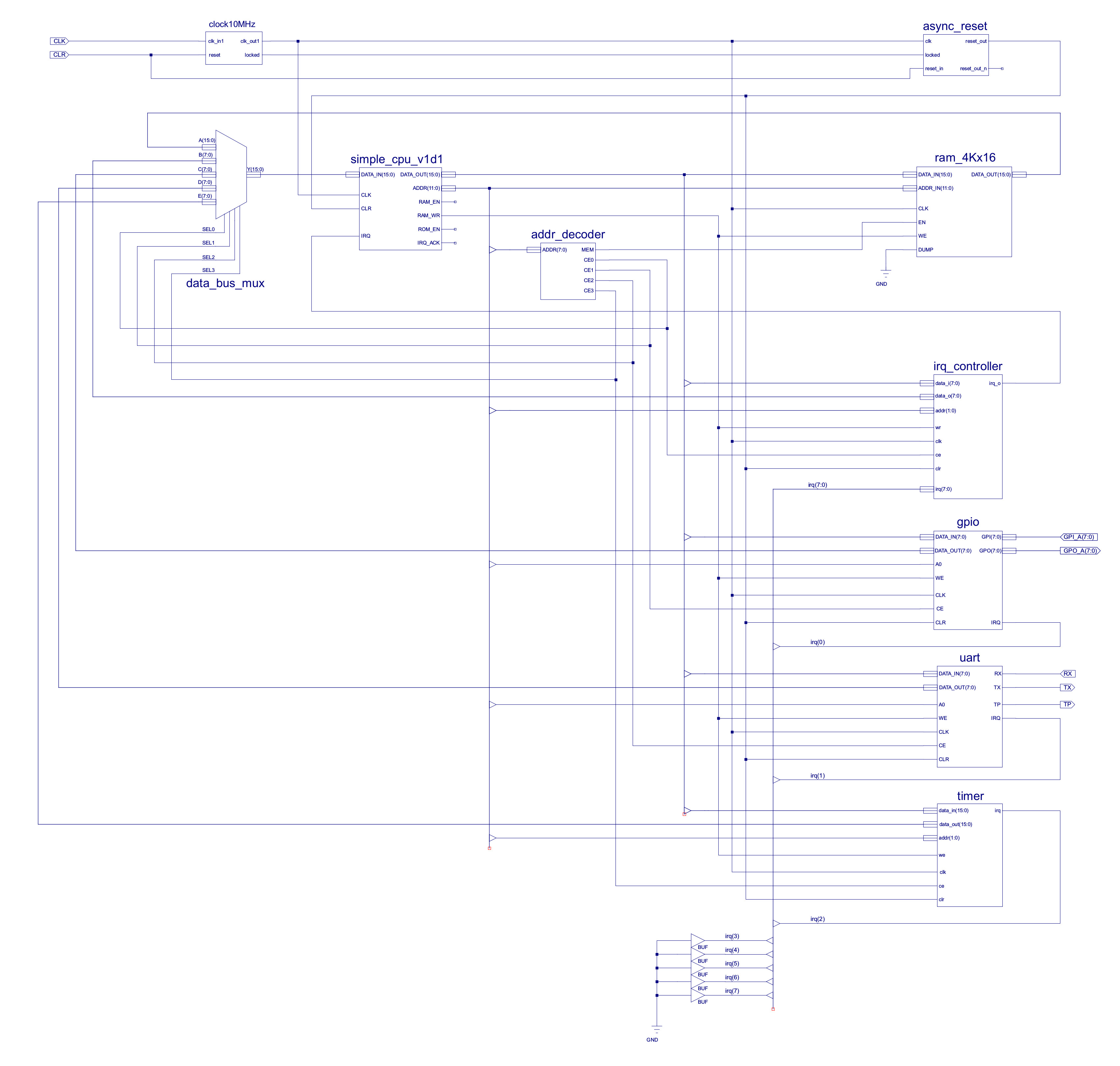
Figure 18 : simpleCPU interrupt controller
Each of these peripheral devices has one or more internal registers, as listed below:
INTERRUPT CONTROLLER
--------------------
ADDR    READ                 WRITE
00      trigger register     clear trigger source register
01      status register      clear status register
10      NU                   NU
11      command register     command register
GENERAL PURPOSE INPUT / OUTPUT PORT (GPIO)
------------------------------------------
ADDR    READ                 WRITE
0       input port           output port
1       output port          output port

IRQ set when input port non-zero
SERIAL PORT (UART)
------------------
ADDR    READ                 WRITE
0       status register      TX data
1       RX data              TX data

UART : status register
----------------------
Bit 7 : nu
Bit 6 : nu
Bit 5 : nu
Bit 4 : nu
Bit 3 : nu
Bit 2 : TX idle (0=False, 1=True)
Bit 1 : RX idle (0=False, 1=True)
Bit 0 : RX data valid (0=False, 1=True)

IRQ set when RX character received, buffer depth 1 char i.e. stores previous CHAR whilst RX the next, then overwritten.
TIMER
-----
ADDR    READ                 WRITE
00      status register      counter register
01      command register     command register
10      status register      NU
11      NU                   NU

TIMER : status register
-----------------------
Bit 7 : nu
Bit 6 : nu
Bit 5 : nu
Bit 4 : nu
Bit 3 : nu
Bit 2 : terminal count
Bit 1 : zero & enabled
Bit 0 : zero

TIMER : command register
------------------------
Bit 7 : clock select msb
Bit 6 : clock select
Bit 5 : clock select
Bit 4 : clock select lsb
Bit 3 : nu
Bit 2 : nu
Bit 1 : single shot (0) or auto reload (1)
Bit 0 : enable count (1=true, 0=false)

TIMER : clock pre-scalar
------------------------
"0000" : clock_div_2
"0001" : clock_div_4
"0010" : clock_div_8
"0011" : clock_div_16
"0100" : clock_div_32
"0101" : clock_div_64
"0110" : clock_div_128
"0111" : clock_div_256
"1000" : clock_div_512
"1XXX" : not used

IRQ set when counter reaches a count of zero i.e. the transition to zero generates the IRQ not a count of zero.
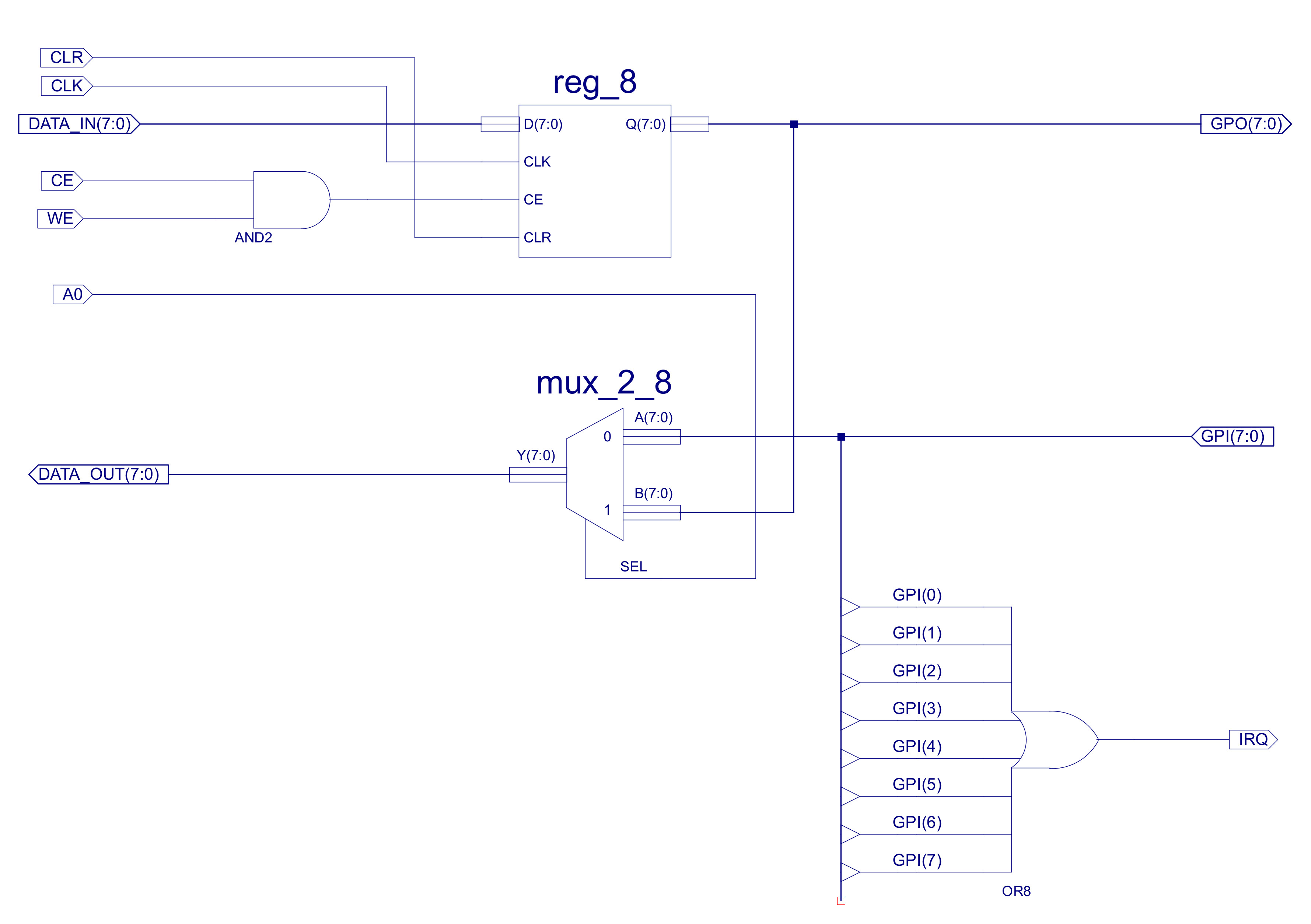
Figure 19 : updated GPIO port
These registers are mapped into the processors's address space as shown in figure 20.
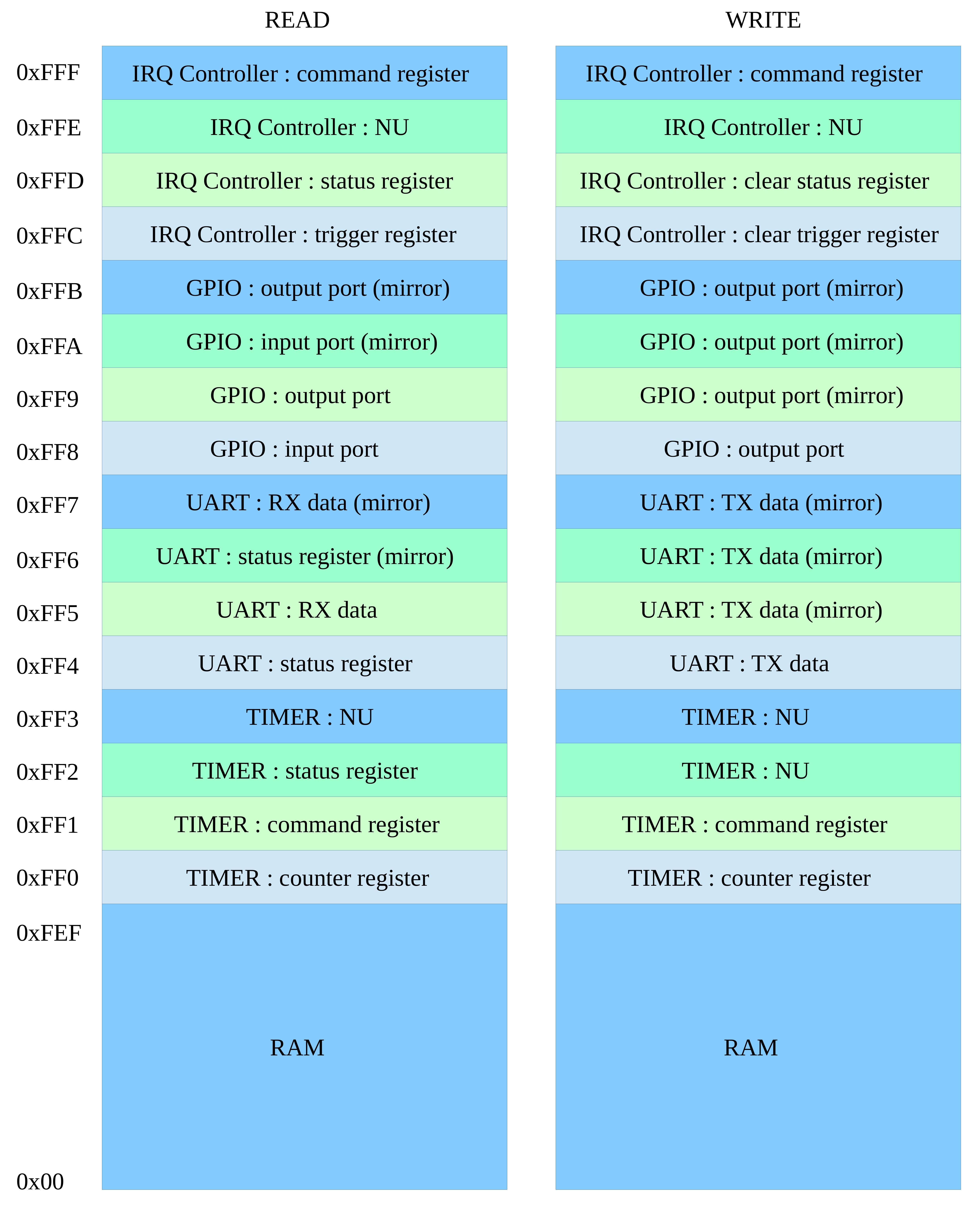
Figure 20 : address map
To simplify coding these addresses are represented using macros:
define(IRQ_CMD,      `0xFFF')
define(IRQ_STATUS,   `0xFFD')
define(IRQ_TRIG,     `0xFFC')
define(GPIO_OUTPUT,  `0xFF9')
define(GPIO_INPUT,   `0xFF8')
define(UART_RX,      `0xFF5')
define(UART_TX,      `0xFF5')
define(TIMER_STATUS, `0xFF2')
define(TIMER_CMD,    `0xFF1')
define(TIMER_CNT,    `0xFF0')
A simple test program :
start:
    move ra 0x07               # 0
    store ra IRQ_CMD           # 1
    load ra CNT                # 2
    store ra TIMER_CNT         # 3
    move ra 1                  # 4
    store ra TIMER_CMD         # 5

wait:
    move ra 0                  # 6
    jump wait                  # 7

isr:
    load ra IRQ_TRIG           # 8

    move rb ra                 # 9
    and rb 1                   # 10
    jumpnz gpio                # 11

    move rb ra                 # 12
    and rb 2                   # 13
    jumpnz uart                # 14

    move rb ra                 # 15
    and rb 4                   # 16
    jumpnz timer               # 17

    reti                       # 18

gpio:
    load ra GPIO_INPUT         # 19
    store ra GPIO_OUTPUT       # 20
    jump isr                   # 21

uart:
    load ra UART_RX            # 22
    store ra UART_TX           # 23
    jump isr                   # 24

timer:
    load ra CNT                # 25
    sub ra 0x10                # 26
    store ra CNT               # 27
    store ra TIMER_CNT         # 28
    move ra 1                  # 29
    store ra TIMER_CMD         # 30

    jump isr                   # 31

CNT:
    .data 0xFF                 # 32
The GPIO port is the same as the existing GPIO port, with the small modification/addition of the eight input OR gate as used in figure 11 i.e. the IRQ output pin is updated to a logic 1 when any of the input pins are set to a logic 1, as shown in figure 19. The UART is the same as previous implementations generating an interrupt when a character is received. The TIMER peripheral contains a 16bit count-down counter, generating an interrupt when the loaded count value is decremented to zero. The TIMER is configured via the command register to operate in single-shot or automatic modes i.e. a single interrupt or periodic interrupt. The 16bit counter in this TIMER is driven by a pre-scaler i.e. another counter, allowing longer time delays e.g. if the clock select bits within the command register are set to "1000" then the "max" / "min" time delays are :
MAX
---
(2^16) * (1/10,000,000) * 512
65536 * 0.0000512 = 3.3554432 seconds

MIN
---
1 * (1/10,000,000) * 512
1 * 0.0000512 = 51 us
Alternatively, if the command clock select bits are set to "0000" the "max" / "min" time delays are:
MAX
---
(2^16) * (1/10,000,000) * 2
65536 * 0.00002 = 0.0131072 seconds = 13 ms

MIN
---
1 * (1/10,000,000) * 2
1 * 0.0000002 = 0.2 us
Note, for longer delays multiple interrupts can be used in combination with software variables e.g. to implement a Real Time Clock (RTC) recording minutes, hours, days, weeks, months, years etc. Shorter delays using the minimum clock select value "000" will be significantly affected by the overheads associated with performing the ISR i.e. each instruction delays the program by 3 * 0.0000001 = 0.3 us. For these types of very short delays application specific hardware or hand crafted software delays would be required.
The TIMER peripheral is initialised with a starting value written into the TIMER_CNT register. The TIMER is then started by setting bit-0 of the command register to 1. Note, whilst this value is being decremented a different value may be written to the TIMER_CNT register without resetting the timer. Writing a logic zero to command bit-0 will stop the timer, writing a logic one to bit-0 will restart the timer. When the count reaches zero and command bit-0 is set to one, an interrupt will be generated. If command bit-1 is set the initial count value is automatically reloaded, otherwise, the TIMER waits for command bit-0 to be updated before restarting the counter.
In the above test program the interrupt vector is set to address 0x008 (hardware in PC). When the GPIO input port changes, this value is stored on the output port. When a serial character is received, this character is retransmitted back to the source. Finally, when the TIMER count reaches zero, the CNT variable is decremented by 0x10 and loaded back into the TIMER i.e. the timer interrupt period decreases, then roll overs back to 0xFFFF, producing a sawtooth interrupt rate.
To show this system in action consider the waveform diagrams shown in figures 21 - 23. In figure 21 the GPIO input port is updated, each logic 1 on the input port generating an IRQ. Note, the IRQ controller is level sensitive i.e. if the input port has a non-zero value multiple interrupt requests will be generated. In figure 22 the UART receives the characters 1,2,3,4 ..., these are received by the UART and retransmitted back using the UART's ISR. In figure 23 the TIMER counter is loaded with the value 0xFF, 0xEF, 0xDF ..., to produce a series of decreasing time delays.
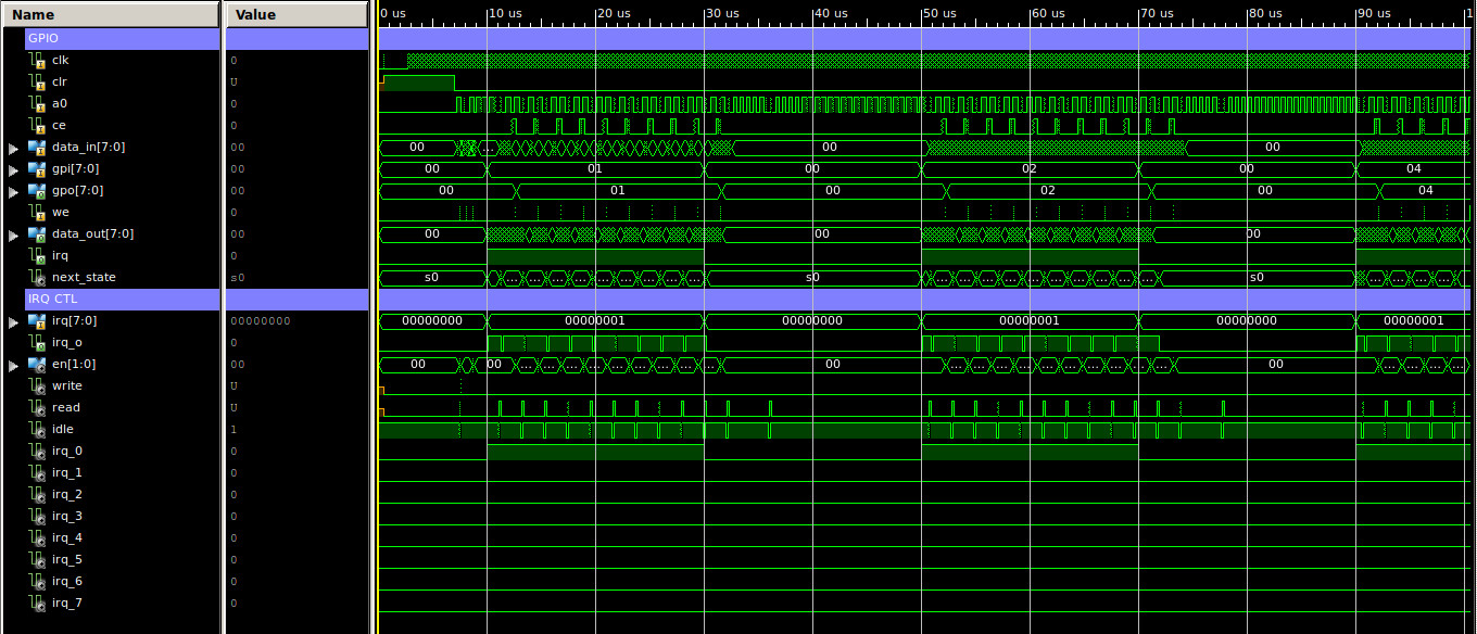
Figure 21 : GPIO waveform diagram
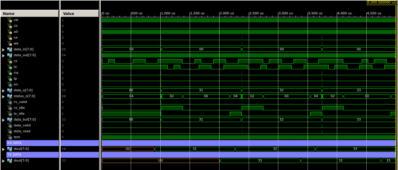
Figure 22 : UART waveform diagram
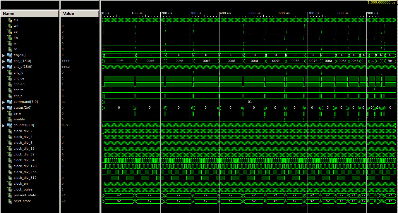
Figure 23 : TIMER waveform diagram
WORK IN PROGRESS

This work is licensed under a Creative Commons Attribution-NonCommercial-NoDerivatives 4.0 International License.
Contact email: mike@simplecpudesign.com