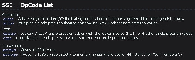
Gone are the days of the general purpose processor, you probably have to go back to the 1980's to find a processor that was _not_ designed for a specific application domain. The problem is that different applications have different processing requirements e.g. in terms of IO, data types, software structures and algorithms, so designing a processor that will maximise processing performance of any given program is a big ask. This can be seen in the rolling development of CISC processors. Using these types of architectures its very easy to keep adding new instruction set extensions e.g. SSE shown in figure 1, that utilise additional hardware units to optimise the processing performance of specific tasks. However, taking this approach a program's performance is only improved if it can use these new instructions / hardware.
Figure 1 : SSE instructions
The examples shown in figure 1 focus on Single Instruction Multiple Data (SIMD) type instructions (Link) e.g. performing four floating point ADDs in one instruction. Unfortunately, not every program needs to perform this type of data processing, therefore, the hardware associated with these new instructions would be wasted for these programs. Eventually, you end up paying for hardware in the CPU that is never used. Alternatively, we could use other optimisation techniques, such as pipelining (Link) and instruction level parallelism (ILP) (Link) that do offer a more general purpose hardware acceleration, but again this flexibility comes at a hardware cost. Therefore, rather than trying to develop the ultimate general purpose processor we have seen a move to application specific processors (ASP), processors designed for specific types of problem.
To continue the development of the simpleCPU family we are going to now focus on an architecture designed for simple image processing algorithms. I've chosen this area as its a nice way of highlighting how the processing performance of different software structures / algorithms can be optimised through the addition of different instructions, addressing modes and hardware units, whilst also giving some nice visual feedback via input and output images. Also, when things go wrong you produce some strange and interesting output images, computer generated art :).
Below is a discussion of how this processor was designed, as always the first step is to identify what types of data the processor will be processing, then develop an instruction-set and hardware architecture to match. The new and improved ISE project files for this computer can be downloaded here: (Link).
How do we represent numbers? In mathematical numbering systems, the base or radix is the number of unique digits (including zero) that a positional numeral system uses to represent a number. The decimal system is most commonly used by humans, base ten, the maximum number a single digit can reach is 9, after which additional digits must be added to represent larger numbers e.g. the value 427 shown in figure 2. Note, the subscript is the base i.e. in this example 10 for decimal.

Figure 2 : Decimal representation
As we use decimal numbers every day we sometimes forget what these symbols actually represent. Each digit represents the base base raised to a power, for the decimal representation shown in figure 2, that is the number of 1s, the number of 10s and the number of 100s etc. Another base that humans commonly use is base 60 e.g. 60 seconds in a minute, 60 minutes in an hour. Therefore, following the same rules we can represent the same number in base 60, as shown in figure 3.
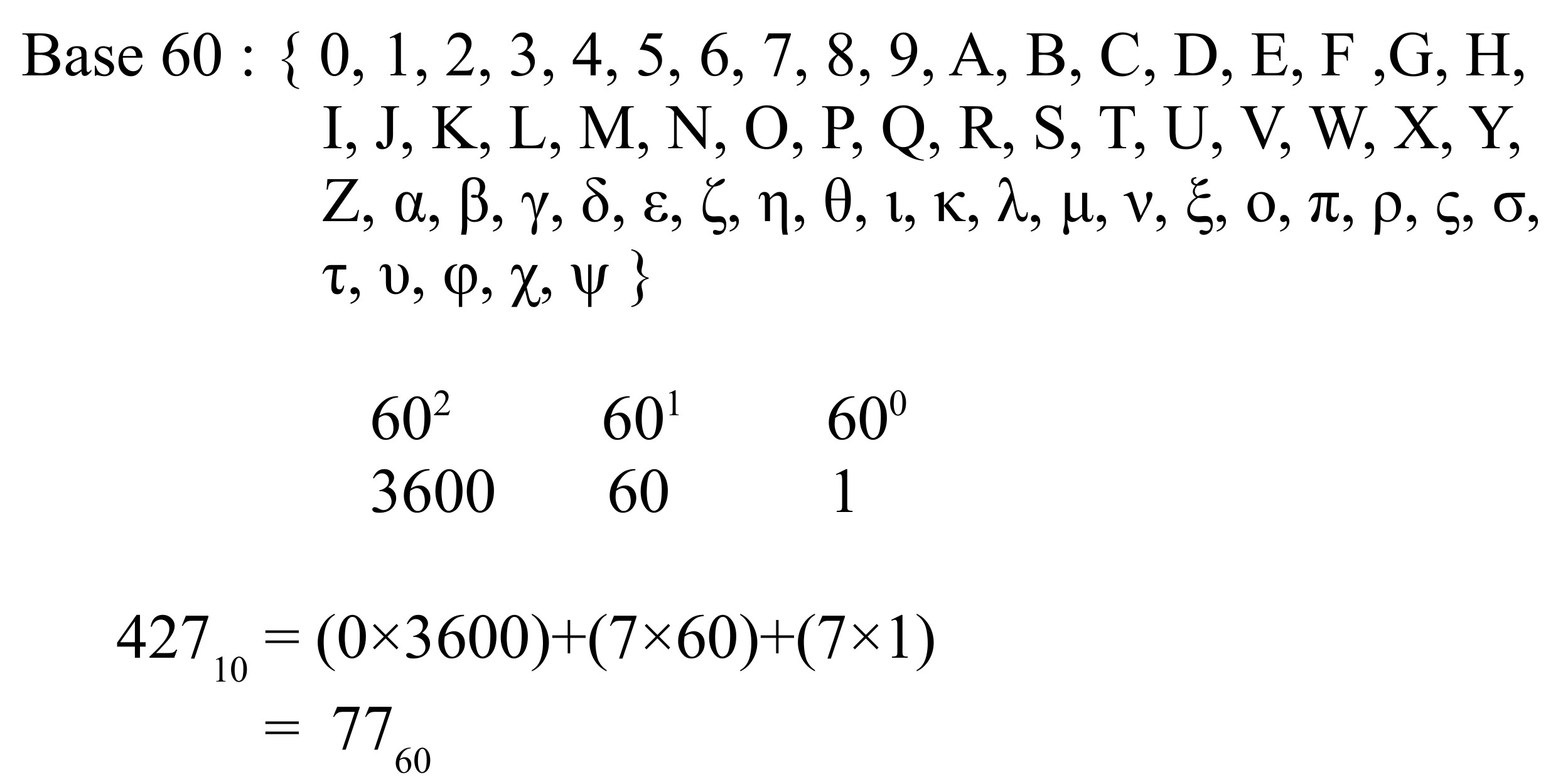
Figure 3 : Base 60 representation
Note, when working in a higher base we typically use the same symbols for 0 to 9, then add on the alphabet for the higher symbols e.g. 10=A, 11=B, 12=C etc. If we still need more symbols, then users choice. The thing to remember when you are working in a different base is that you apply the same rules as you would for decimal, but rather than the maximum value a digit can reach being 9 it will be the base-1 e.g. in base 60 the maximum value a digit can represent is 59. The value of the number has not changed in these examples its still a count of 427, the move to a higher base just means that each digit can now represent more symbols, therefore, we need less digits to represent the same number.
When you think of a computer you naturally think of a binary representations, base 2 (Link), as shown in figure 4. Note, each binary digit being called a "bit". Some early computers actually used a decimal representation even though internally they used a digital "binary" technology e.g. ENIAC (Link) etc. Number base selection depends on a number of different factors: human interface, usability, memory requirements, processing overheads etc, but one of the main requirements is to match the selected number base to the technology used. The transistor technologies used in modern computers naturally have two operating states: on or off i.e. discrete mode. They can be operated in a continuous mode to represent more states, however, this dissipates significantly more power in the transistors i.e. they would get even hotter. As this technology naturally supports two states, the most efficient number base to use is base 2, or binary. Note, remember there is nothing special about base two, if transistors had three stable states we would use base 3, you are always looking to minimise cost and power by selecting the most efficient implementation.
In a computer each binary digit used to represent a number is transferred on a separate wire. The state of each digit i.e. 1 or 0, is assigned a voltage level, as shown in figure 5. This figure shows the typical voltage range (0V to +5V) for a TTL logic gate (Link). Note, this is an old logic standard, as transistors have got smaller the voltages used have also reduced, but the same principles apply for more modern ones.
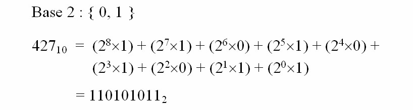
Figure 4 : Binary representation
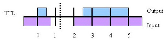
Figure 5 : TTL logic levels
The assigned output voltage range is shown in BLUE (variations due to manufacturing tolerance), this is the voltage level driven onto a wire. The input voltage range is shown in PURPLE, this is the voltage level received at the other end of the wire. The input voltage range overlaps the output voltage range i.e. the noise margin. This voltage difference is a key factor in the success of binary computers. Whenever you build a machine, be it mechanical or electrical, their will be noise i.e. small errors in how a digit is represented, by only using two voltage levels we can have a wide separation between these voltages, meaning that significant levels of noise would be required to accidentally change a logic 0 into a logic 1 or vice-versa. This makes binary computers very resilient to internal or external noise sources i.e. you would need to add quite a lot of energy to increase or decrease the voltage level on a wire to flip the bit.
To process these binary numbers we use Boolean logic gates, as shown in figure 6. I always find this a strange one i.e. how binary numbers are processed using Boolean logic gates. Obviously a base two number, made up of the numerical digits 1 and 0 are not the same as Boolean TRUE and FALSE i.e. they are fundamentally different data types. We can encode a 1 as TRUE and a 0 as FALSE, but, if you stop and think about it, performing a logical operator on a number feels odd e.g. 1 AND 1, what are you actually doing when 1 is a number? For the moment we can ignore this question and focus on their use in the computer :)

Figure 6 : Boolean logic gates
Note, remember a number has three attributes: base, symbols (used to represent a digit's value) and the physical realisation (voltage levels). However, a number is still a number, no matter what base, or technology used.

Figure 7 : Representing a number
To convert a number from the human world (base 10) to the world of the computer (base 2) we follow the same rules as for decimal numbers. We write out the powers of the base i.e. 2^0, 2^1, 2^2 etc, calculating their numerical values i.e. 1, 2, 4 etc. Then through the process of repeated subtraction we can obtain the binary representation, as shown in figure 8. To convert a binary number into a decimal representation you just reverse the process as shown in figure 9.
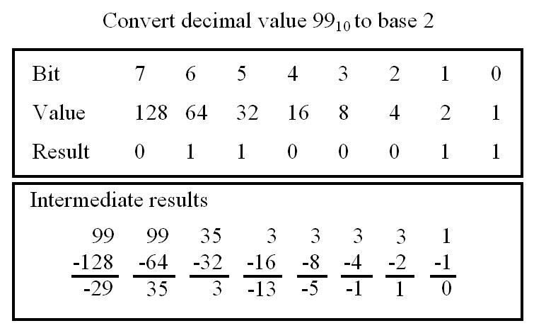
Figure 8 : Converting decimal to binary
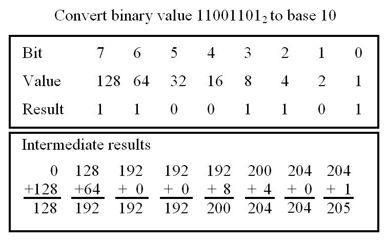
Figure 9 : Converting binary to decimal
The move from a higher to a lower base i.e. base 10 to base 2, means that we need more digits to represent the same value, as each digit now represents less symbols. When designing or selecting a processor one of the first considerations taken is how many bits do we need to represent the data / values we will be processing. The maximum and minimum values that an unsigned number can represent is given by the equation :
max = +(2^N)-1
min = 0
where N is number of bits, the symbol "^" reads as "to the power". Version 3 of the simpleCPU is intended to process images. To identify each element that makes up the picture i.e. a pixel (Link), the processor will need to assign it an address in memory. Even a small images need a significant number of bits to store each pixel e.g. if an image only has 100 x 100 pixels then we will need to represent the value 10,000 which will require 14 bits:
(2^8)-1  = 255
(2^9)-1  = 511
(2^10)-1 = 1023
(2^11)-1 = 2047
(2^12)-1 = 4095
(2^13)-1 = 8191
(2^14)-1 = 16383
(2^15)-1 = 32765
(2^16)-1 = 65535
Note, as discussed previously, negative numbers are typically represented using a 2s complimented representation (Link), a key thing to remember is that if you go to a signed representation you loose a bit (MSB becomes the sign bit), therefore, the maximum value you can now represent is halved. The maximum and minimum values that a signed number can represent is given by the equation :
max = +(2^(N-1))-1
min = -(2^(N-1))
Taking all of this into consideration, to allow room for the program and data i.e. images and intermediate values generated as they are processed, the address bus width will need to be expanded from the existing 8 bits. How big depends on what your doing. The aim of this new processor is to demonstrate simple image processing techniques, i'm not looking to design a processor to process HD images. Also, form a teaching point of view the bigger the image the slower the simulation speeds, so smaller images are better for lab work. Image data will be approximately 100 x 100 pixels, as shown in figure 10, these are 97 x 60 pixels (scaled up a bit for this web page).


Figure 10 : Image data: 97 x 60 = 5820 pixels, black and white (left), colour (right)
Working with this type of data will require the processor to uniquely identify at least 5820 pixels, which is a lot larger than the original simpleCPU's 8 bit address bus can do i.e. can only address 256 memory locations. However, before we can work out the size of the new processor's address and data busses i.e. the maximum values that we will need to represent, we need to understand how the images shown in figure 10 are stored in the processor's memory.
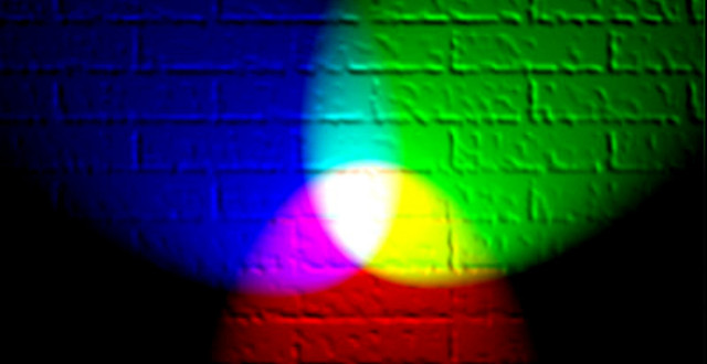
Figure 11 : Colour - Red, Green, Blue
How do we represent images? When you enter the land of image processing you soon find out that there are actually quite a few way of representing the different colours we see in an image, each with its own advantages and disadvantages. Perhaps one of the most common models used is the RGB colour model, were each colour is defined as a mixture of the three primary colours Red, Green and Blue, as shown in figure 11. In this example (Link) we have the three primary colours projected onto a white wall, the overlap of these lights produces the secondary colours: yellow, cyan and magenta. The addition of all three colours produces white, the absence of all three colours produces black, varying the intensities of these primary colours will produce all the colours of the rainbow.
To represent the colour of each pixel we need to store its R, G and B values. The intensity of these colours are typically represented by an 8 bit value i.e. 0 = none, 255 = full. Therefore, to store this image data in memory we will need 8+8+8 = 24 bits for each pixel. A nine pixel image (3x3) is shown in figure 12, requiring 9 x 24 = 216 bits, or 27 bytes. Each row is a different primary colour, varying in intensity: 64, 128 to 255.

Figure 12 : 3 x 3 pixel image
This raises the question of how we should structure external (RAM) and internal (Registers) memory to efficiently process this data. External memory data widths are normally allocated in 8 bit blocks, therefore we could structure memory such that each memory location stores an:
As the most commonly accessed data type from memory will be pixel data e.g. reading through an image array, a 24 bit data width will be selected, to maximise performance, minimising overheads in read and writing this data from/to memory. This may result in wasted memory when storing other data types, numbers used by the processor etc, but as these will occur less frequently this should have a minimal impact on memory efficiency i.e. wasted bits. Now that the data bus width has been decided we can calculate the address bus width. Since each memory location can store one pixel i.e. R, G and B, we will need 100 x 100 = 10,000 memory locations for each image. When processing images we may need to generate intermediate images and output images. We will also need to reserve space for the program and other variables. Therefore, it was decided to go for a 16 bit address bus, this will give the processor: 65536 x 24 bit = 196,608 bytes of storage, which should be sufficient for our needs, maybe :). Note, at this stage these decisions are best guesses, the machines performance is still dependent on a number of other factors.
In addition to considering external memory data widths, we also need to consider how this data will be stored and processed within the processor. The previous versions of the SimpleCPU used a single 8 bit general purpose register i.e. the accumulator. Therefore, selecting a wider external data bus width would not make sense unless we also modified the internal storage. To store these new 24bit values in the CPU we will also need 24 bit registers. As we may need to process each of the R, G and B colour elements we will also need more than one general purpose register, otherwise the CPU will have to read and write a lot of intermediate values to memory, negating the advantage gained in moving to a 24 bit data bus i.e. reading all three RGB elements in one memory transaction is only an advantage if the CPU can use this data. The number and size of the general purpose registers in the CPU is again very dependent on the type of algorithms used. Note, another consideration to keep in mind is that the number of general purpose registers will also have an impact on the instruction size and format e.g. if there are two registers we would need to add an addition two bits to identify operand source and result destination. This is an important considerations as these instructions will also need to be accessed across the processor's data bus i.e. if the instruction is bigger than 24bit it will have to be stored across two memory locations. Note, as you design a processor you soon become aware that every element is tightly coupled, a small change in one place can have a big impact in others.
To allow us to decide on how internal CPU components should be structured we need to know the types of operations that will be performed and the data that will be processed e.g. if you add two 8 bit numbers together you could generate a 9 bit result, if you multiply two 8 bit numbers together you could generate a 16 bit result. The R, G and B values of each pixel are 8 bit values, therefore, you could argue that the ALU's arithmetic and logic units only needs to process 8bit data. However, this data focused view does not consider an algorithms requirements e.g. a common operation performed in image processing is Convolution (Link). A process in which each pixel within an image is altered by the weighted sum of its neighbours, normally used to filter out noise, detect edges, features within an image etc. This process requires multiplication and the accumulation of a number of values, therefore, the ALU's data width needs to be large enough to process these intermediate values e.g. consider the arithmetic mean shown in figure 13.
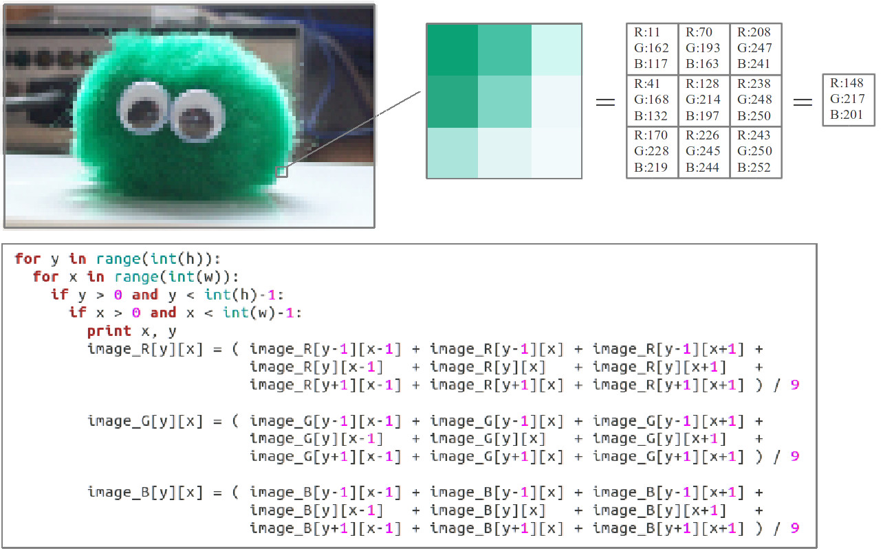
Figure 13 : Mean filtering
Mean filtering (Link) is commonly used to smooth pixel transitions, remove noise within an image. In this example we are using a 3x3 matrix i.e. summing the centre and surrounding pixel values (within a 3x3 block) for each colour and then taking the average to produce a new value for the centre pixel. If we repeat this process for every pixel (ignoring the outer rows and columns) you would produce the new image shown in figure 14. Note, the new image is smoothed, blurred, reducing sharp transitions, edges etc.

Figure 14 : Mean filtering, original (left), smoothed (right)
In this example, to calculate each new pixel value the program has to sum nine pixels, potentially having to process the value 255 x 9 = 2295. Note, the size of the matrix could be larger e.g. 5x5, 7x7 etc, increasing this maximum value. The python code used to generate this image and the original image is available below, remember i am an electronics engineer not a software engineer, so take this in mind we considering the quality of the code :).
In addition to considering how image data will be processed we also need to consider how memory will be accessed. In the example python program shown in figure 13 we are using variables X and Y to index through the 2D arrays that store the R, G and B pixel values. In the actual CPU these variables will be resolved into an address in memory i.e. an address pointer, a variable that stores the location of the data that will be processed (rather than the actual data). Therefore, the ALU must be capable of processing these 16 bit address values as this is the size of the processor's external address bus.
To summarise, as you can see when you are designing a processor there are quite a few things to consider. The size of a processor's address bus, data bus and functional units are very dependent on the type applications used. For this version of the simpleCPU the following decision were taken. Obviously the bigger these values are the more processing the processor can do, but this always comes with an associated increase in hardware costs, so a CPU's architecture is always a compromise between cost and performance.
Data Bus                 : 24bits       - pixel data can be fetched in one memory transaction, minimise data access times
Address Bus              : 16bits       - estimated from size of images and program size
ALU functions ADD/SUB    : 16bits       - estimated from algorithm and functional units used
ALU functions AND/OR     : 24bits       - estimated from algorithm and functional units used
Instruction size         : 24bits       - instruction can be fetched in one memory transaction
Data registers           : 24bits x 4   - allowing R, G and B values to be assigned separate registers + "spare", whilst minimising instruction size (limited to 24bits)
A small aside, not used directly by the simpleCPU, but we need to select an image format so that we can store input images to files on the host PC, and generate output images that can be viewed on the PC from the data stored in the simpleCPU's memory. Input images are loaded into the simpleCPU's memory during simulations using a modified version of the VHDL memory model discussed previously: (Link). Output images are also generation by this VHDL simulation model, when the DUMP pin is pulsed high, image data at specified memory locations is written files, stored on the host PC in the simulation directory. The image file format used for both input and output images is the NETPBM image format (Link). The main advantage of this image format is its simplicity, each RGB pixel value is represented in an ASCII text file. This greatly simplifies image creation and editing, as this can be done with a basic text editor.
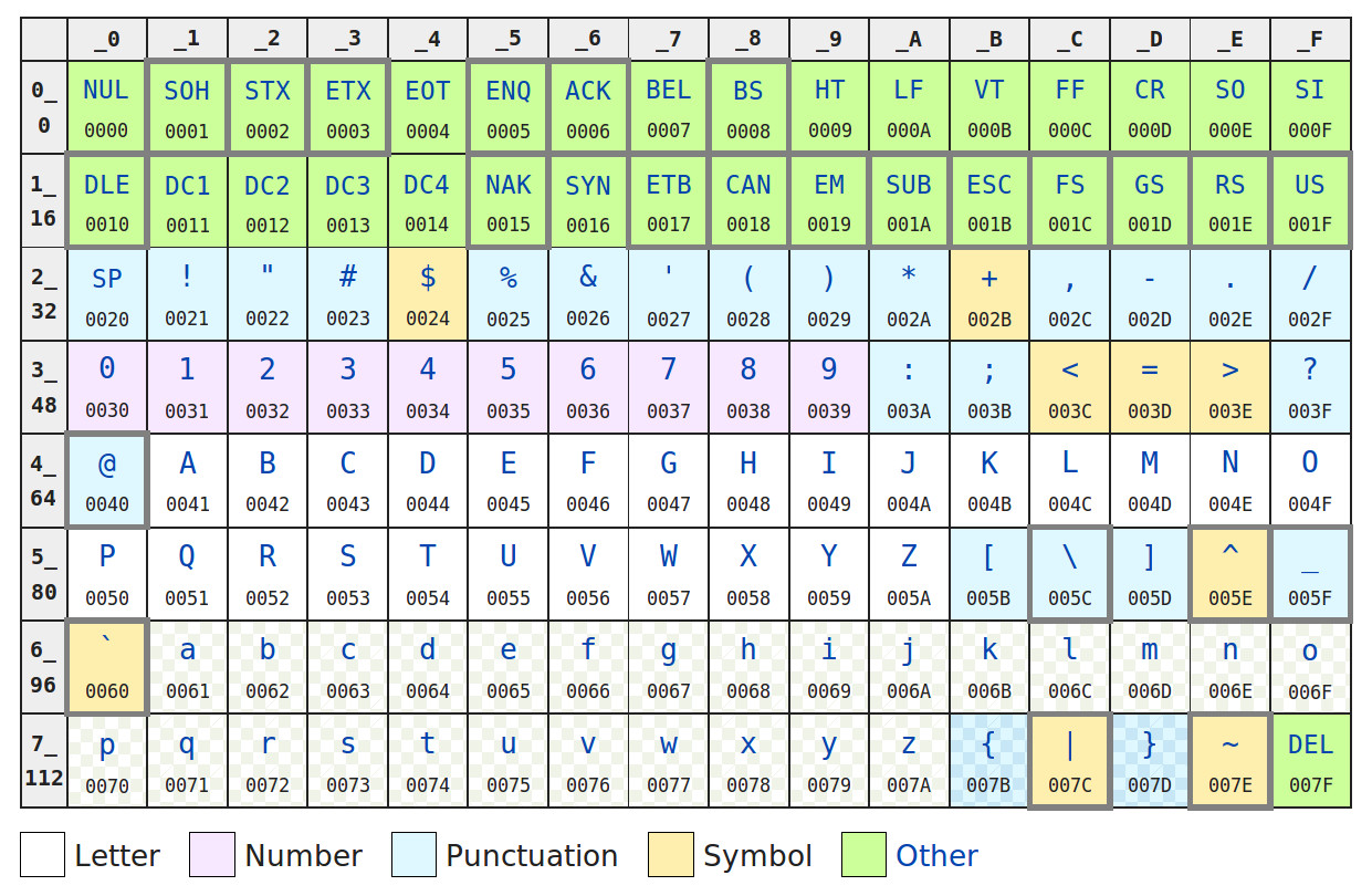
Figure 15 : ASCII encoding
How do we represent text? Letters, numbers, punctuation and other symbols are represented by assigning each character a unique code. One of the most common encoding schemes is the American Standard Code for Information Interchange (ASCII) (Link), as shown in figure 15. This encoding scheme dates back to the first computers, commonly using teleprinters and other communications equipment. These used a 7bit code to represent non-printable control characters i.e. commands that controlled the printer e.g. line feed, carriage return, bell etc, and printable alphanumeric characters. The table in figure 15 shows the hexadecimal (base 16) value of each character from 0x00 to 0x7F. An example text string is shown in figure 16, the text string "Hello World" is passed to the hexdump command-line tool, displaying the hexidecimal value of each character e.g. "H"=0x48, "e"=0x65 etc, terminating with the Line Feed (LF) character 0x0A.
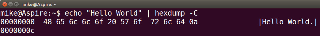
Figure 16 : ASCII text string
Note, these 7bit values only represent the text characters in the computer's memory or file, the symbols displayed on the screen are defined by the font (image) used by the terminal program.
How do we represent images? The Portable PixMap (ppm) (Link) image format was originally designed to send images within plain text emails. The image shown in figure 17 is represented by this text file (Link), listed below. This is a very small 3 x 3 pixel image (scaled for web page).
P3
# CREATOR: GIMP PNM
3 3
255
11  162 117
70  193 163
208 247 241
41  168 132
128 214 197
238 248 250
170 228 219
226 245 244
243 250 252
This image is represented in a plain text file. The first line identifies the image format to the viewer by its "magic" number P3. This is then followed by a comment/description of the file. The next line defines the image size: columns (width) and rows (height). Lastly, the maximum value of each pixel. The remainder of the file defines the RGB value of each pixel. Note, these RGB values are listed sequentially in the file, they do not need to be on the same lines, the number of RGB values on each line can be varied.

Figure 17 : example ppm image
Remember, when interpreting RGB values i.e. what colour does it represent, it is the relative size of each term, rather than their absolute values that count e.g. the last pixel in the image has a very large G term (250), from this you could assume that it would be green, however, as the the R & B terms are of a similar level it actually looks white. For a pixel to appear green the R & B terms will need to be smaller than the G term e.g. the first pixel in the image where G=162, R=11 and B=117.
The hexadecimal dump of this image file is shown in figure 18, showing the ASCII value of each character. The hexadecimal value of each character is listed on the left, and its symbol on the right i.e. the string 255 on the right, the second line down, is not the value stored in memory, rather the three 8 bit character codes 0x32 ("2"), 0x35 ("5") and 0x35 ("5"). Non-printable characters such as Line Feeds (LF = 0x0A) are displayed on the right hand side of the image as "." characters.
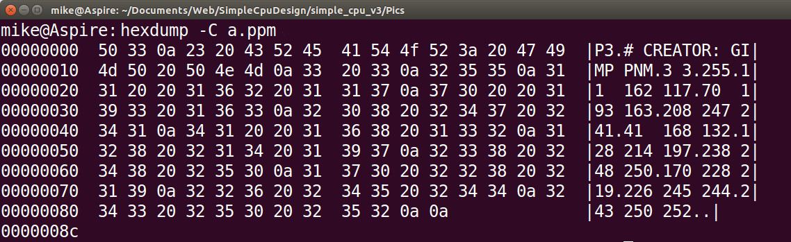
Figure 18 : hexdump of ppm image file
Note, this image is defined as a plain text file, therefore, if you where to edit this file in Notepad or Gedit you can change the colour of any of these pixels e.g. if you change the last pixel i.e. (243, 250, 252), to the value (0, 0, 0) the bottom right pixel would turn black, when this image was next opened in an image viewer e.g. Paint or Gimp. Remember, this is only a 3 x 3 image so you will need to zoom in quite a bit :).
The other image format we will be using is the Portable BitMap (pbm), a black and white image format. Its main advantage over ppm is the reduction in file size, as each pixel is now represented as either a 1 (black) or a 0 (white). This also minimises memory usage in the simpleCPU, as now rather than each pixel requiring three bytes i.e. 24bits, each pixel can be represented by a single bit i.e. each memory location can store 24 pixel values. The image shown in figure 19 is represented by this text file (Link), listed below. This is a very small 5 x 5 pixel image (scaled for web page).
P1
# CREATOR: GIMP PNM
5 5
01110
10001
10101
10001
01110
This image is again represented in a plain text file. The first line identifies the image format to the viewer by its "magic" number P1. This is then followed by a comment/description of the file. The next line defines the image size: columns (width) and rows (height). The remainder of the file defines the pixels state: 1=Black or 0=White. Again, these values are listed sequentially in the file, they do not need to be on the same line, in this example they are arranged 5 x 5 so you can almost see the resultant image.

Figure 19 : example pbm image
Finally, figure 20 shows the hexdump of this image file, from this you can see the size savings i.e. compared to the ppm image file shown in figure 18. Also, just to prove that it is just a plain text file, ASCII 0x30="0", 0x31="1". :).
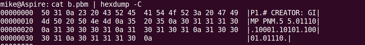
Figure 20 : hexdump of pbm image file
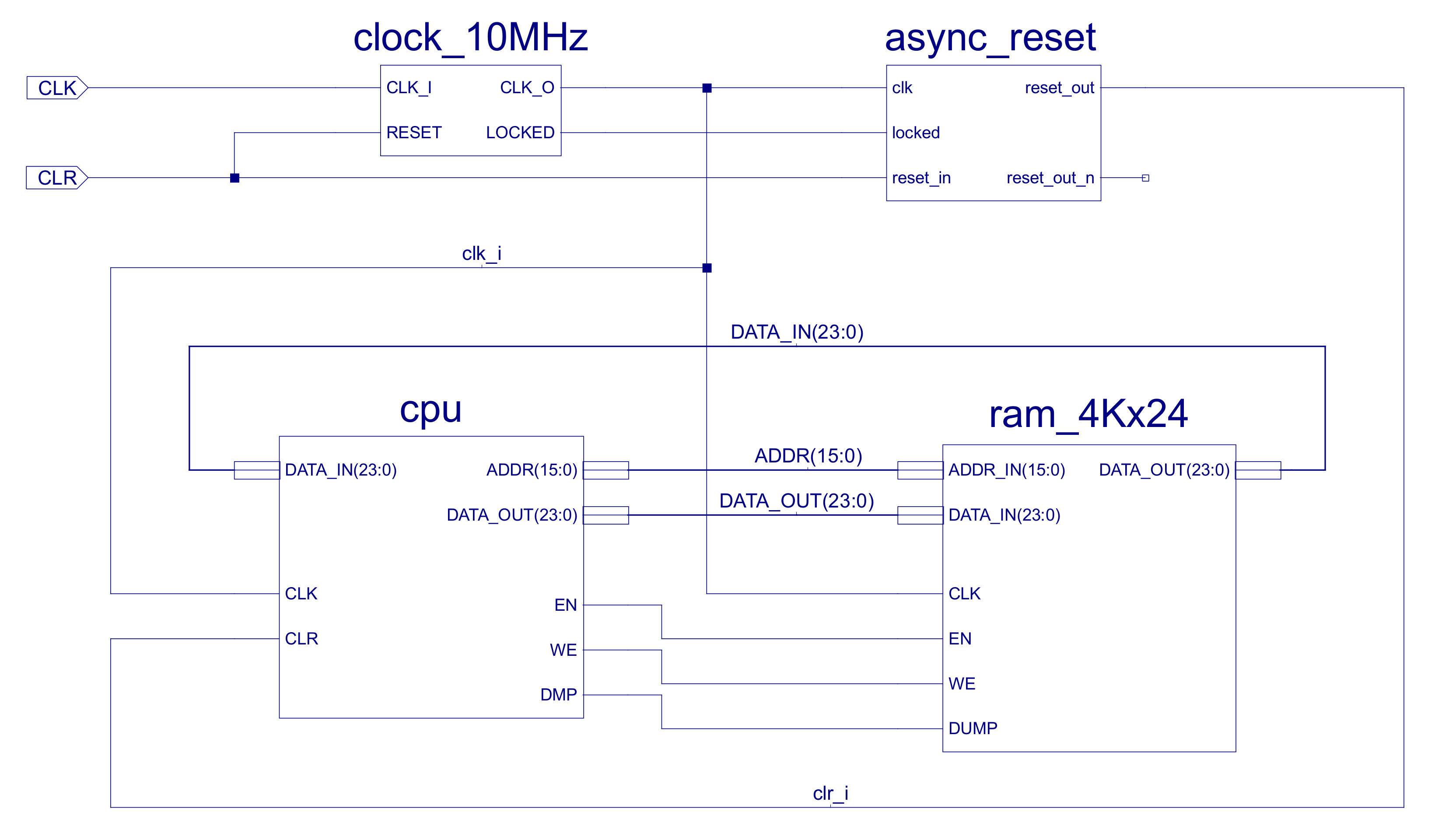
Figure 21 : Top level : computer
The top level view of the simpleCPU v3 is shown in figure 21, the only notable changes are to the data and address busses, now 24 bits and 16 bits respectively. The first big improvement is to the processor's instruction set needed to implement the new image processing algorithms i.e. both in terms of functional units and addressing modes. This has a big impact on the design decisions taken regarding the CPU's instruction format, but, one decision made early on was to keep a fixed length instruction as this simplifies the instruction fetch phase.
Note, remember when you start to add more instructions, the opcode field will naturally get bigger, increasing instruction length/size. All normal processors need to implement the basic MOVE, ADD, JUMP type instructions, these simple instructions tend not to need a large number of bit fields to encode their functionality. As we add more complex instructions these will tend to need more operand fields etc, so will further increase the required instruction length. This raises a similar problem as discussed when selecting the processor's data bus width. If we set the instruction length to the size of the longest instruction, simple instructions will not need all these bits, therefore, again you will waste memory i.e. unused bits in the instruction. To overcome this we can set the instruction length to the size of the smallest instruction and spread longer instructions other multiple memory locations i.e. a variable length instruction format. However, this makes identifying where each instruction starts and stops in memory a lot more tricky, increasing the complexity of the fetch/decode hardware e.g. what do you increment the PC by?
Therefore, the starting point for this new instruction set is a fixed length 24 bit instruction. When designing an instruction format its all about comprises i.e. what do you need and how can we get it to fit within the specified instruction size. As always, i'm sure if you were to give this task to ten different engineers you would get ten different solutions, each with there own advantages and disadvantages, so here we go ...
The current version of the simpleCPU v1a has a 4 bit opcode field i.e. it can support 16 different instructions. Note, remember this is not 16 different functions, you also need to consider the addressing mode used i.e. you may have many different ADD instructions, sourcing their operands from memory, registers, or immediate values, each will require a different opcode. Therefore, the opcode field will need to be increased to 5 or 6 bit i.e. to allow 32 - 64 different "function + addressing mode" instructions. Note, to save space the opcode bit field does not need to be in the same position for each instruction, we can make use of unused bits within the instruction. However, for the moment to keep the hardware simple we will place the opcode in the the top 6 bits of the instruction.
As discussed previously, to allow the RGB elements to be processed in the CPU we need more general purpose data registers. This will again increase the instruction length as previous we only had one general purpose register, the ACC i.e. it was implicit where one operand was coming from and where the result would go, therefore, we did not need to encode this within the instruction. Moving to two or more data registers will need the addition of source and destination bit fields. How many registers do we need? To start with i'm going to go with four: RA, RB, RC and RD. Why four, well its a best guess given the algorithms that could be used, the size of the opcode field and the immediate values needed. Therefore, we will need 2 bits to select source and destination registers.
The next decision is how many operands each instruction should be support? Consider the instructions below:
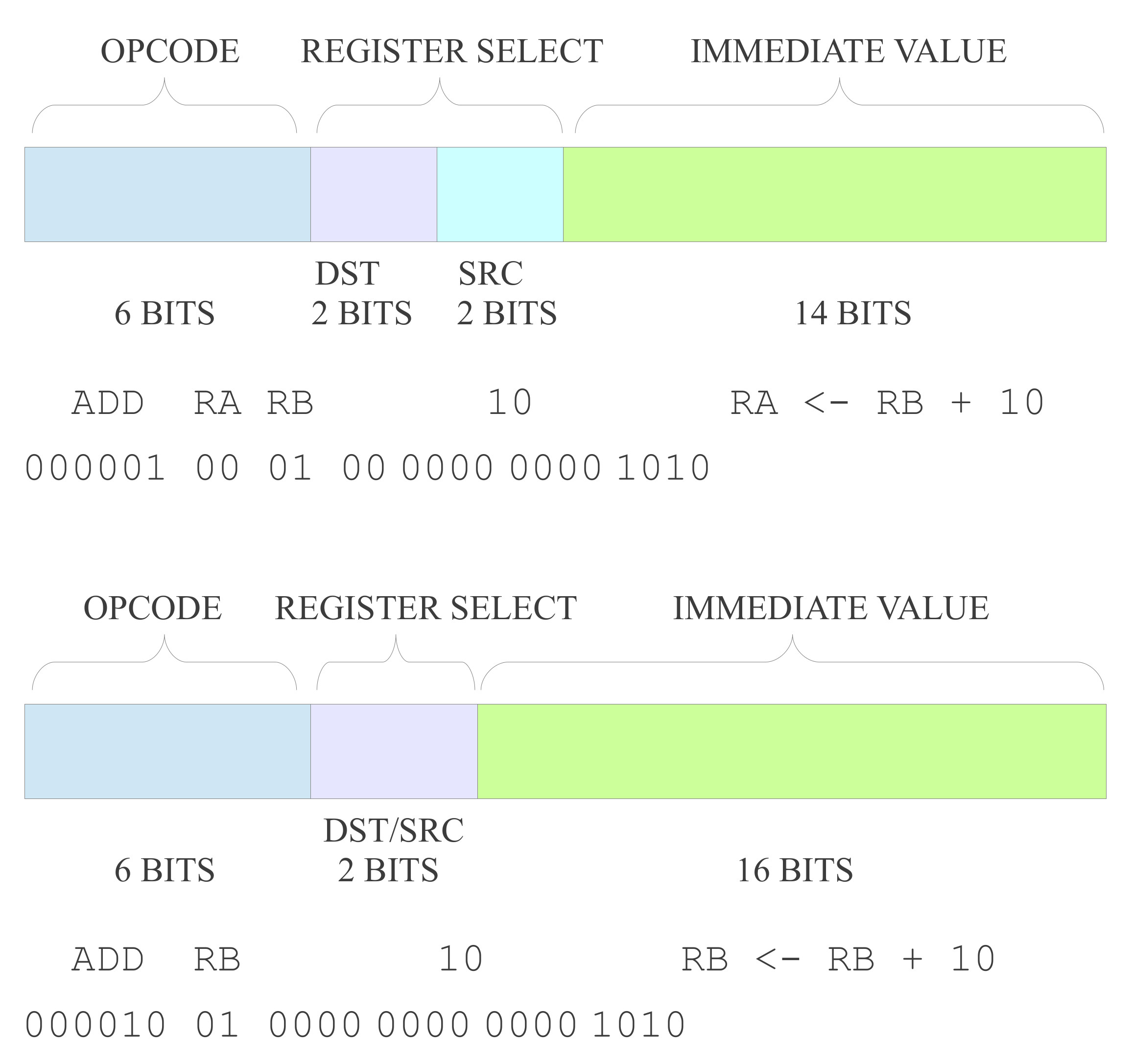
Figure 22 : Immediate addressing mode - 3 (top) or 2 (bottom) operand format
These instructions performs an immediate ADD using a constant and a register. The result of this addition can be stored in a different register (top) or the same register as the original source (bottom), overwriting the original value. Given the fixed length instruction format and opcode field length these two options will limit the maximum size of the immediate value within the instruction to: 14 bits for 3 operands, 16 bits for 2 operands. The 3 operand instruction format is a nice-to-have, as it gives you the most flexibility in deciding what data is stored within the processor. We could support both of these instructions formats, assigning each a different opcode e.g. as was done in early VAX computers (Link). However, as always this flexibility comes at the cost of hardware. Another thing to consider is the types of data that will be processed. A 14 bit immediate value will be large enough for most of our needs, except for when it comes to processing addresses, as the address bus for this CPU is 16 bits. Therefore, i decided to limit instructions to the two operand format, such that we could specify a full 16 bit address within an instruction. Note, again there are ways around this problem e.g. we could use the 14 bit value as a relative offset from the current PC value, but again this adds a bit of complexity to the hardware, if you can get away with it, its simpler to specify the full absolute address.
The addition of the four general purpose registers allows a new addressing mode: register addressing. Consider the instructions below:
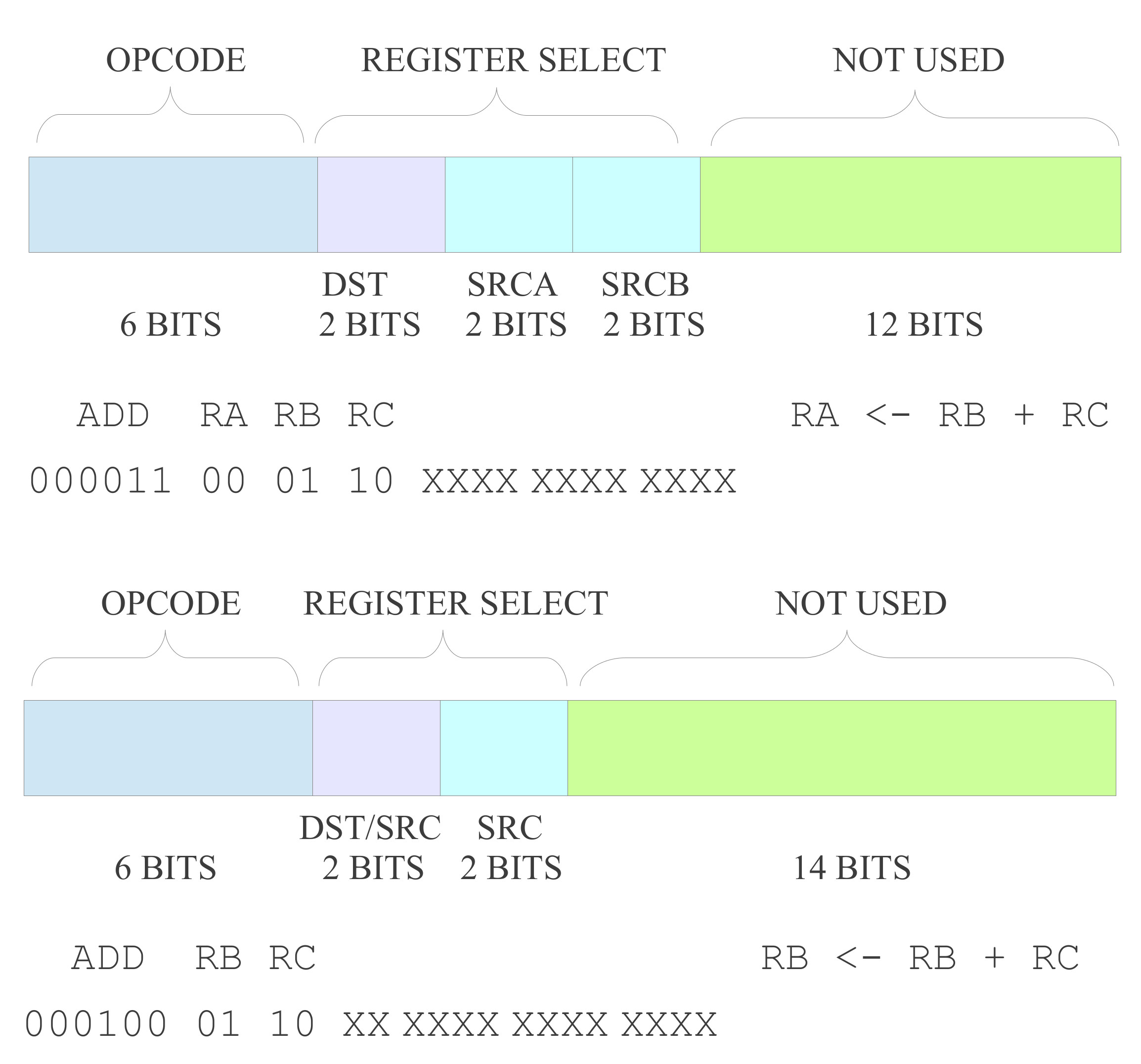
Figure 23 : Register addressing mode - 3 (top) or 2 (bottom) operand format
As all operands are now stored in registers the number of bits required to encode these instructions reduces significantly i.e. the instruction only need to identify the registers used rather than their data values. As a result we have quite a few unused bits: 12 for 3 operand, 14 for 2 operand. Therefore, from an instruction length point of view either format can be used, with no impact on functionality. However, again there would be a small hardware cost in supporting the 3 operand format as we would need additional multiplexers to select the correct bit fields. Therefore, again will limit these instructions to the 2 operand format, from a consistency view point.
The final new addressing mode made possible by the addition of more general purpose registers is: register indirect addressing. Consider the instruction below: 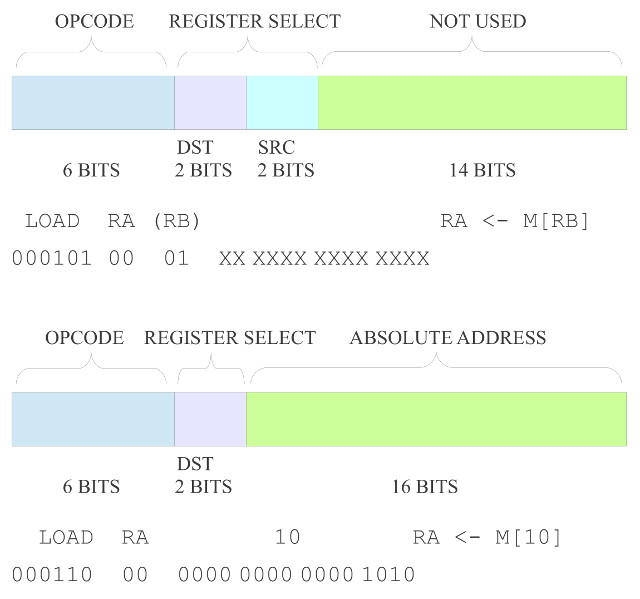
Figure 24 : Register indirect addressing mode (top), absolute (bottom)
In the previous versions of the simpleCPU processor if we wanted to read data stored in memory we would use the absolute addressing mode, as shown in the bottom LOAD instruction in figure 24. This is fine for accessing single variables stored in memory, but if you need to implement a looping software structure to read through an array i.e an image stored in memory, we need a way of updating the address defined in the instruction. In early machines this was done through self modifying code, as described in the previous FGPA implementation of the simpleCPU v1a (Link). However, a program that rewrites itself during run-time is not considered the safest solution to this problem :). Therefore, with the addition of a little more hardware (mostly an additional MUX on the address bus) we can now use the contents of a register as the address, rather than a bit field in the instruction, as shown in the top LOAD instruction in figure 24. Here register RB is used to store the 16 bit address of the memory location we wish to access, rather than the actual data. This is the "indirection" i.e. we need to read the contents of the register to obtain the address of the external memory location we need to read to get the actually data we require. Now, if we need to change this address e.g. to the location of the next pixel, all we need to do is increment register RB. Note, when you see an assembly language instruction and one of the registers is enclosed by round brackets "( )" this is normal an indication that this register is used to store an address rather than a data value.
In addition to these new addressing modes, to allow the CPU to implement a wider range of image processing algorithms, new instructions have been added to the instructions set. These include support for a wider range of conditional jump instructions i.e. to implement different relational operators: equal to, not equal to, greater than, less than greater than or equal to, or less than or equal to, commonly used in thresholding type operations (Link). A wider range of bitwise logic instructions (Link), and as previously discussed in the FPGA implementation of the simpleCPU v1a, a proper CALL / RET subroutine mechanism. The hardware needed to implement this new processor is shown in figure 25. For comparison the original simpleCPUv1 block diagram is shown in figure 26. Note, when you compare the two block diagrams you can see that there is a new register file, but the main addition are the extra multiplexers and internal busses, these are required to implement the new addressing modes supported by the processor e.g. register, register-indirect etc. Each new element is discussed in detail in the following sub-sections.
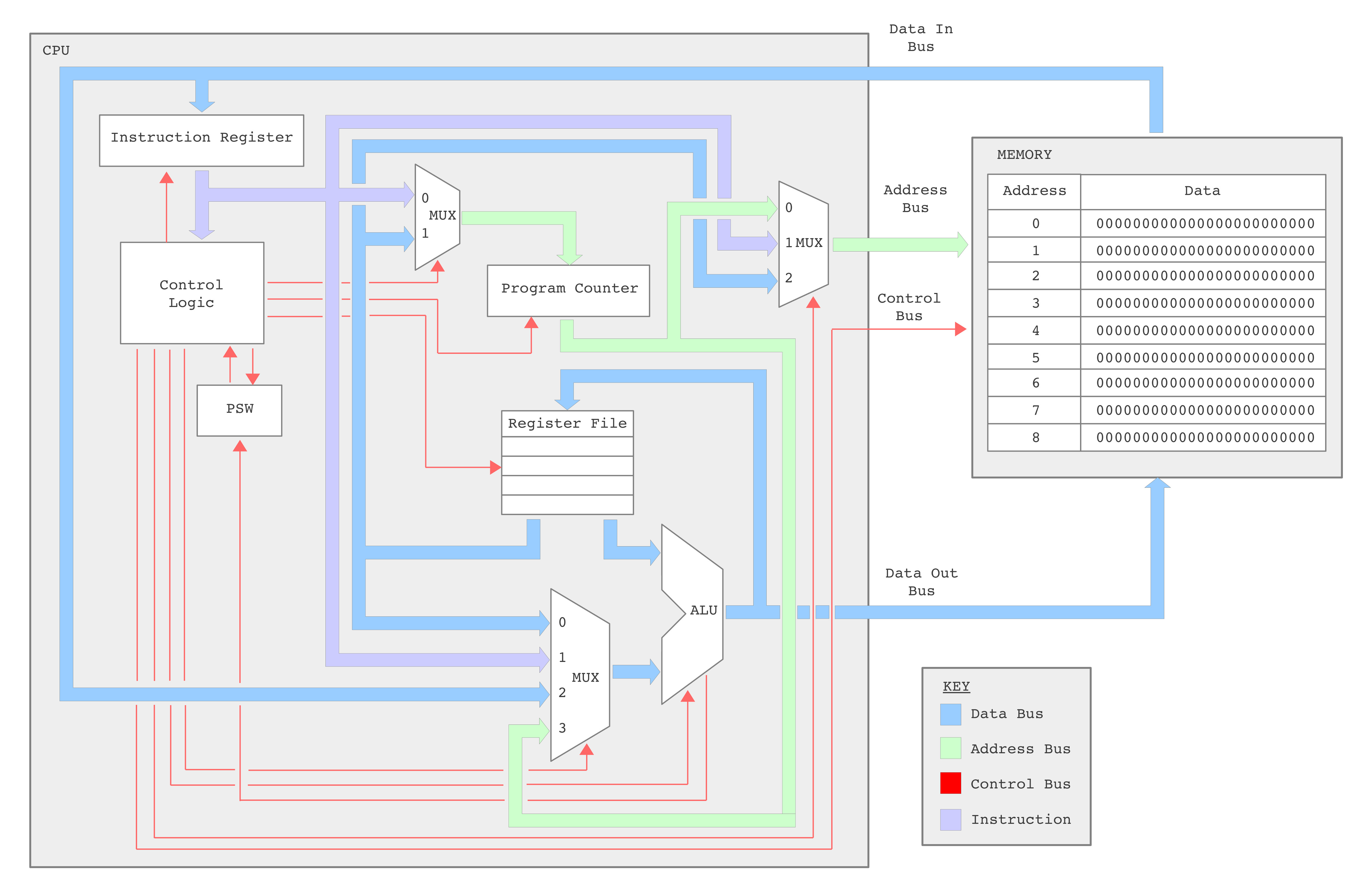
Figure 25 : simpleCPU v3 block diagram (top), schematic (bottom)
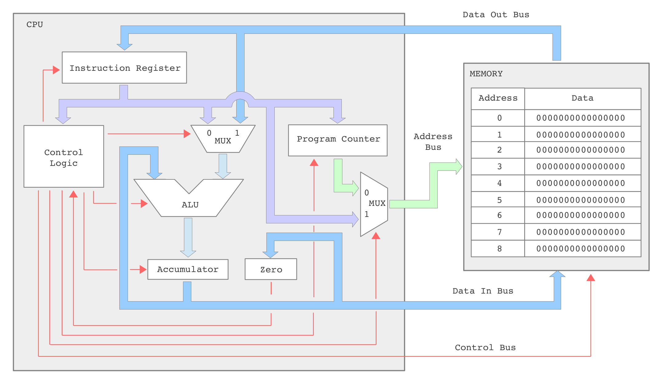
Figure 26 : simpleCPU v1 block diagram
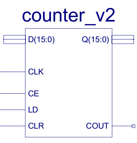
Figure 27 : Program counter (PC)
Not much to say, very much the same as the PC used in simpleCPU v1, its internal components expanded to 16 bits to match the new 16 bit address width.

Figure 28 : Program counter (PC)
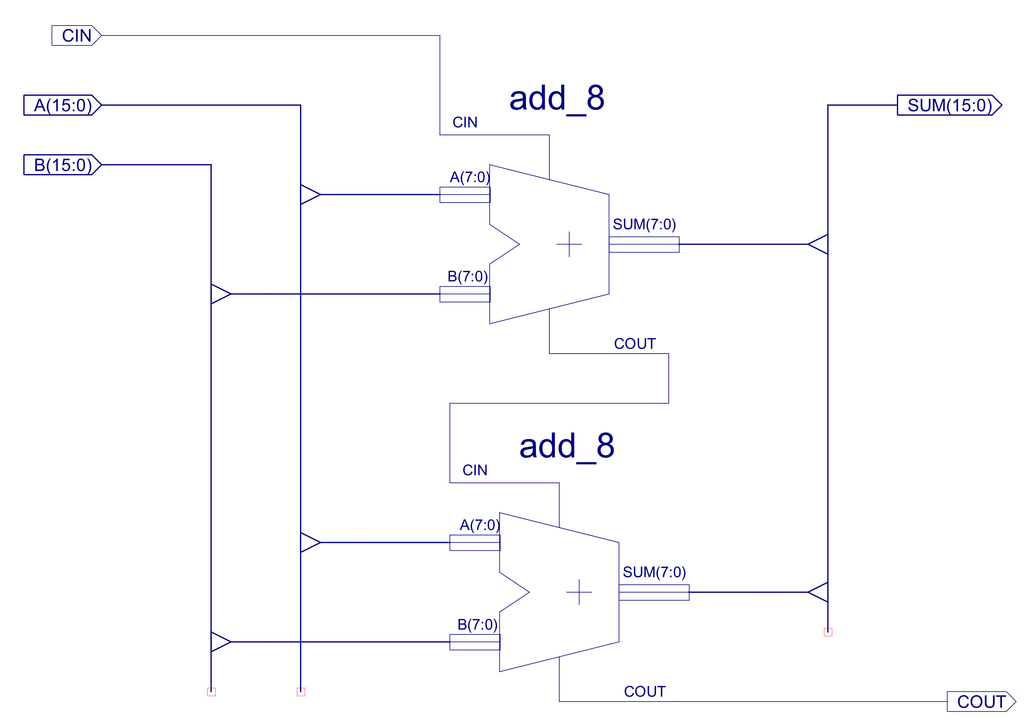
Figure 29 : ADD_16 - adder 16bits
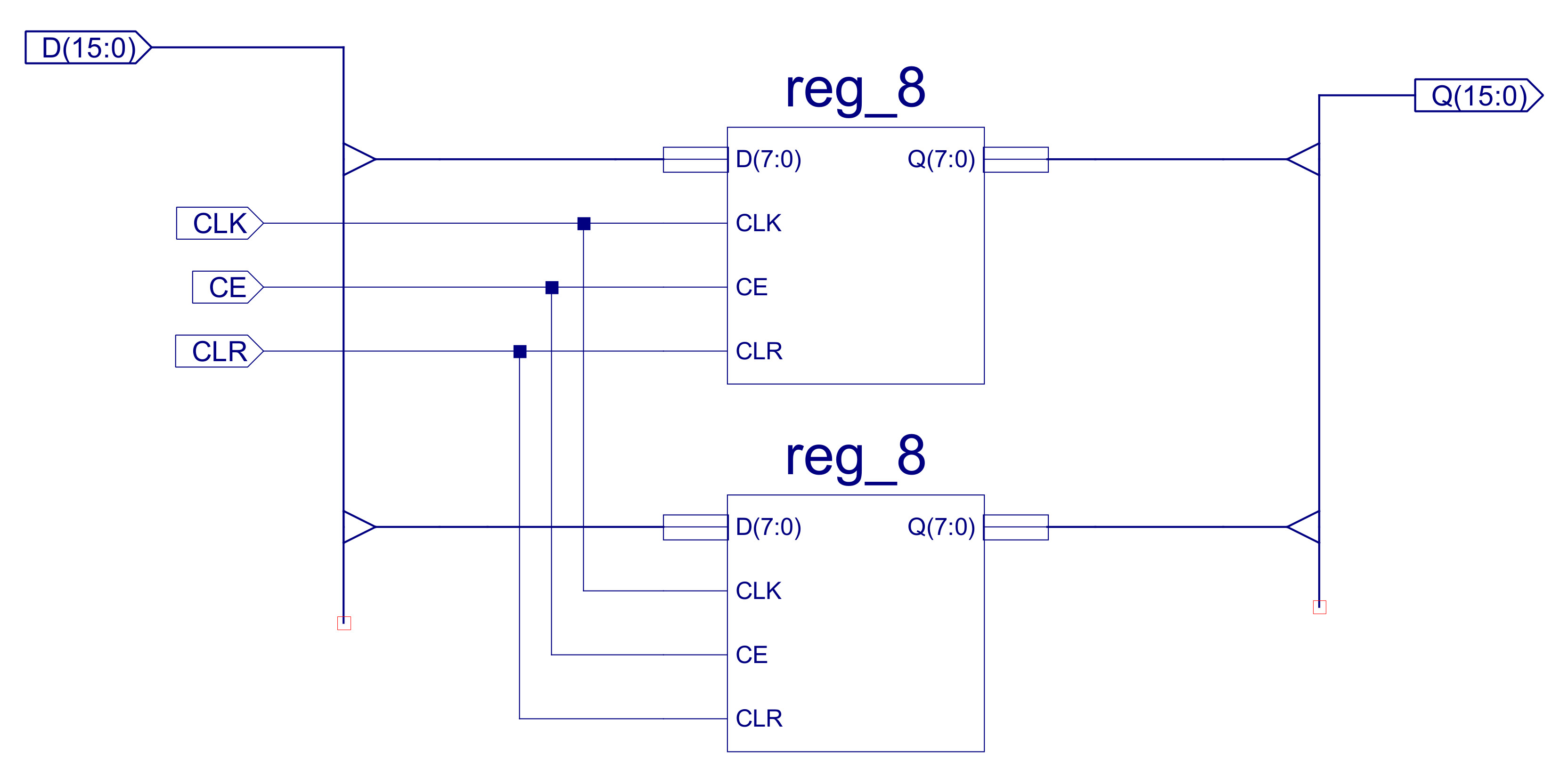
Figure 30 : REG_16 - register 16bits
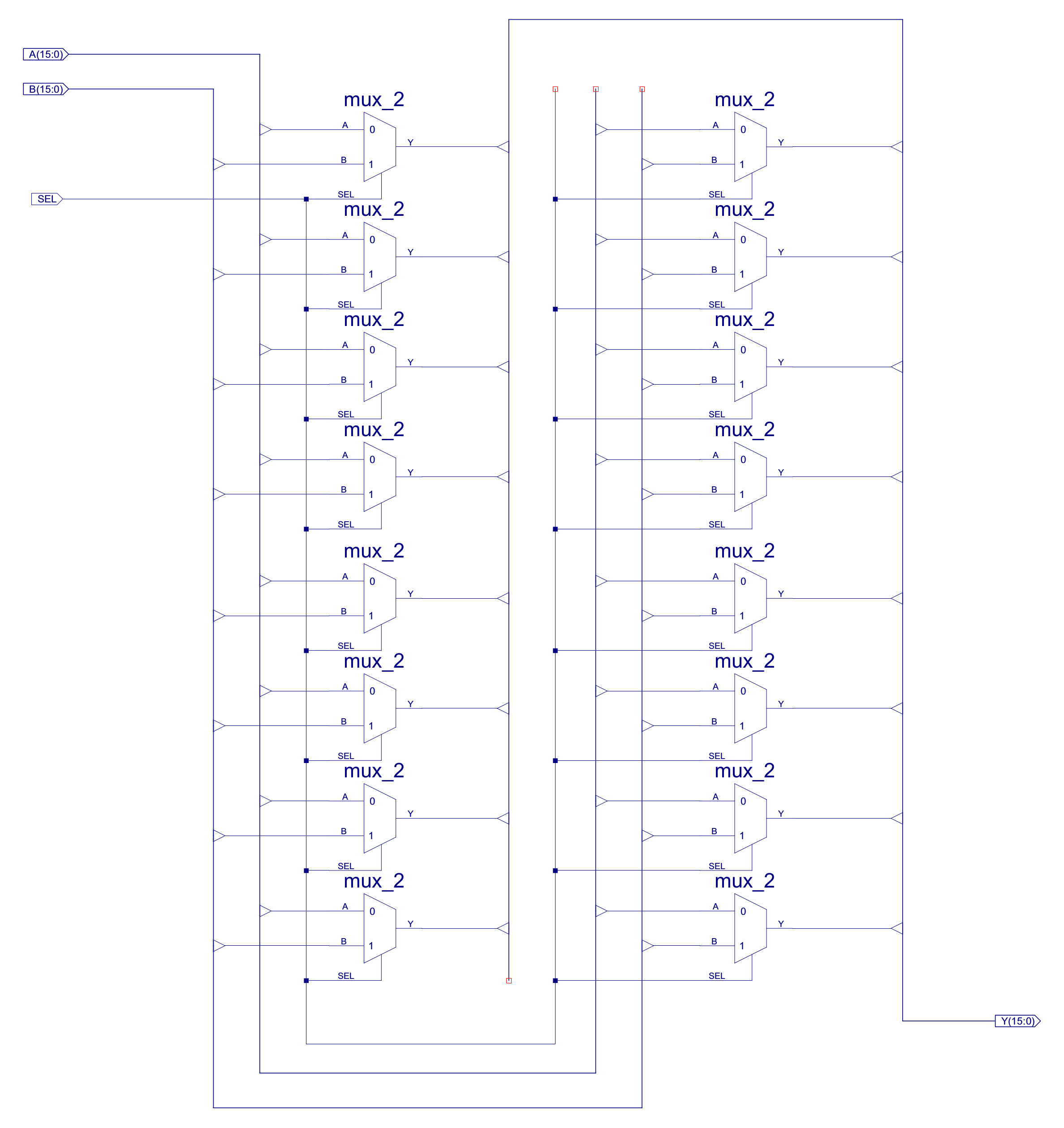
Figure 31 : MUX_2_16 - 16bit x 2-input multiplexer
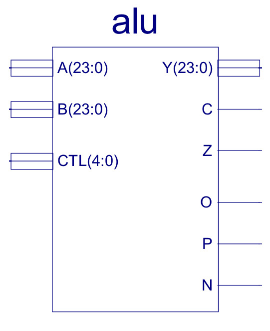
Figure 32 : Arithmatic and Logic Unit (ALU)
Externally, the first obvious difference to the simpleCPUv1's ALU is the increased number of status bits e.g. overflow, carry, positive etc. These are used to increase the range of conditional JUMP instructions. As shown in figure 33 the internal architecture is also similar, but with the increased number of functional units and data widths, the final multiplexer (MUX_8_24) is increased to eight inputs, 24bit data widths. The internal construction of these component are shown in figures 34, 35 and 36.
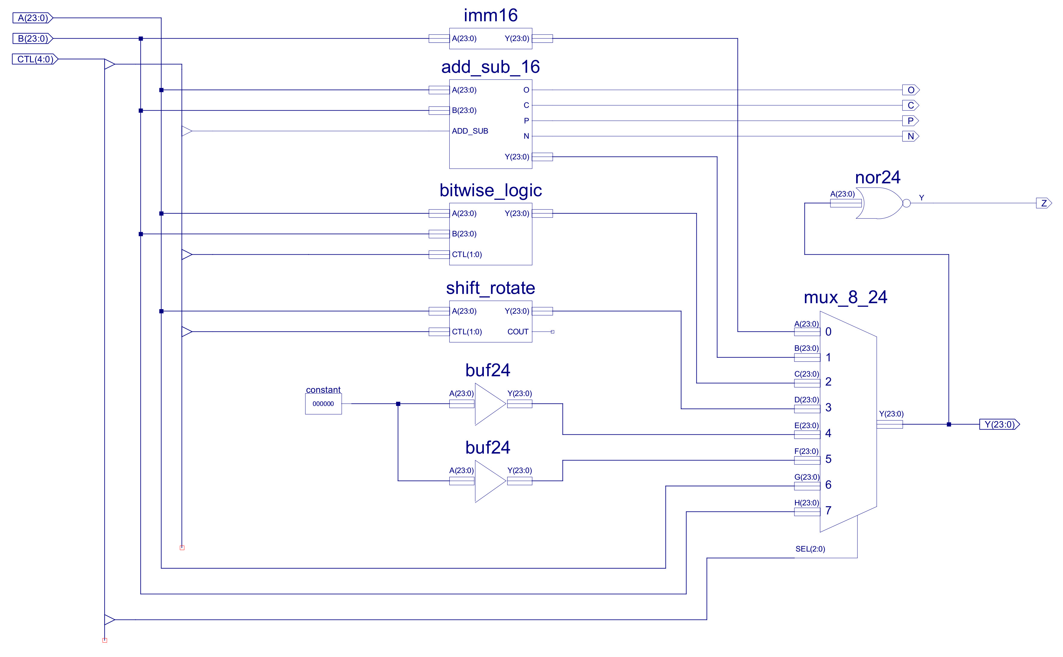
Figure 33 : ALU

Figure 34 : MUX_8_24, constructed from two MUX_4_24 + one MUX_2_24
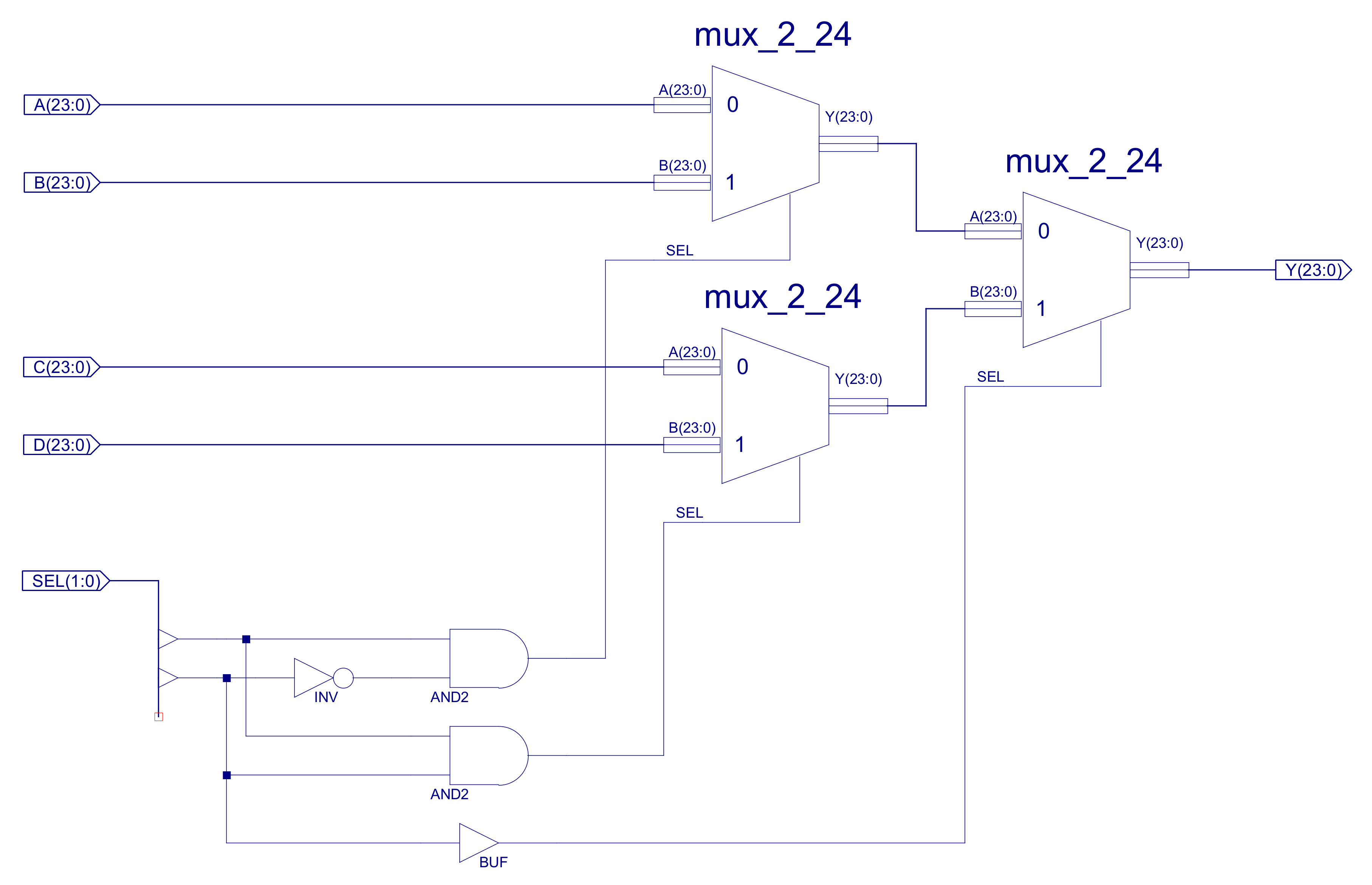
Figure 35 : MUX_4_24, constructed from three MUX_2_24
The output of the MUX_4_24 multiplexer is controlled by the small logic circuit shown in figure 35, using inputs SEL(1:0):
SEL(1) SEL(0)  Y
  0      0     A
  0      1     B
  1      0     C
  1      1     D
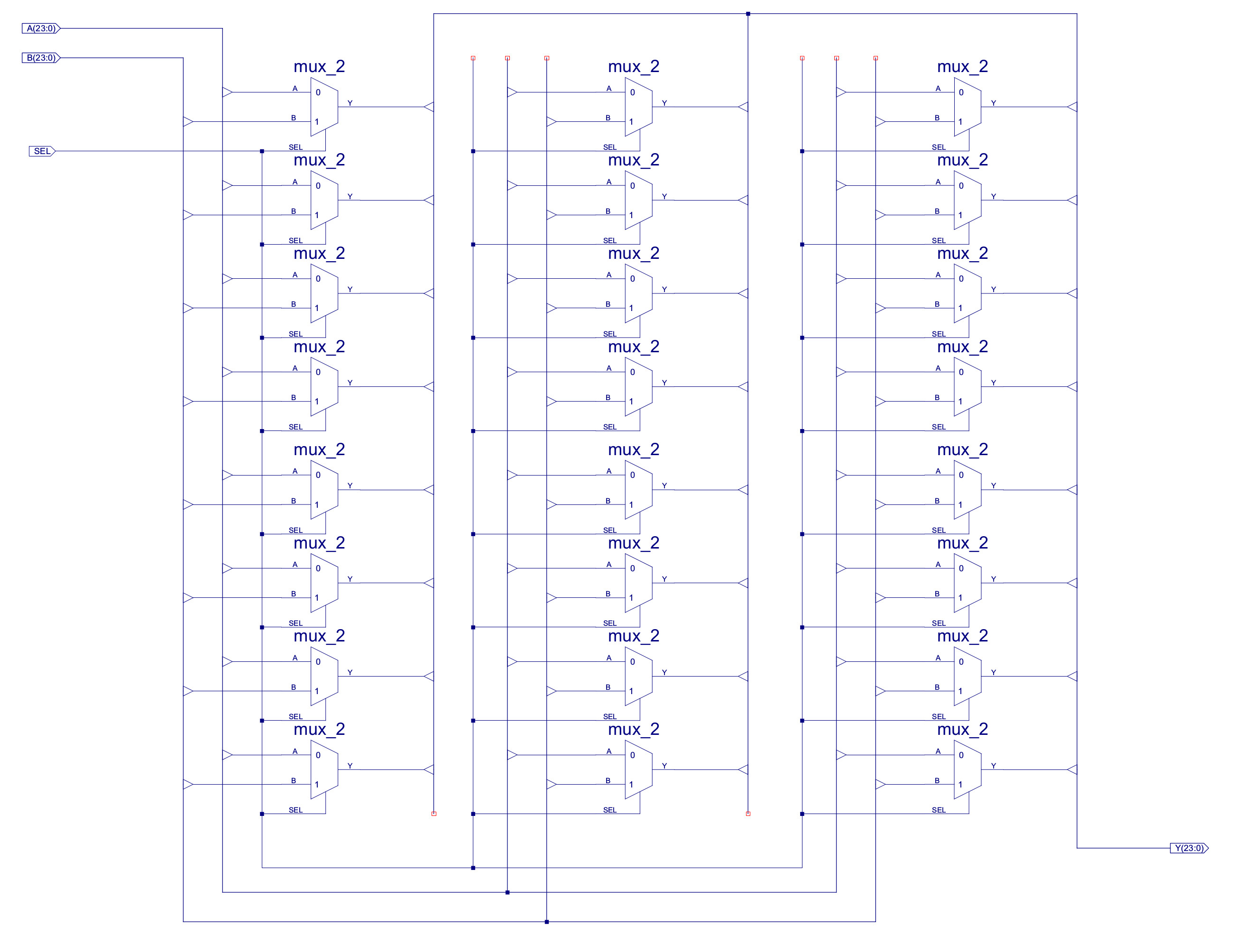
Figure 36 : MUX_2_24 - 24bit x 2-input MUX constructed from twenty-four 1bit x 2-input MUXs
The ALU input and output busses are 24 bit, however, the adder-subtractor is limited to 16bits, as previously discussed (data types used). Therefore, the top byte of input busses are masked off (not used) and high nibble of the output bus is hardwired to zero i.e. Y(23:16) = "00000000", as shown in figure 38. Note, rather than fixing these high bits i could of replicated Y15 i.e. sign extended this number to 24 bits. This could of had a few advantages, but, for the present going to keep things simple and zero these bits. The C (carry out) status bit is the COUT of the final ripple adder stage: C15, set high when the adder produces a 17 bit result i.e. an overflow, a result that can no longer be processed by the adder. Note, as previously discussed when using 2's compliment i.e. signed data types, the C status bit does not indicate an overflow, as shown in figure 37. The calculation 150 + (-44) will set the adders COUT line, however, this calculation has not generated an overflow. Therefore, the C status bit should only be used for instructions that have processed unsigned data types. The O (overflow) status bit is the "carry" signal for signed arithmetic calculations. In signed arithmetic an overflow is determined by these rules:
Examples of these rules are shown in figure 37. These rules are implemented by the XNOR, XOR and AND gate network shown in figure 38. The P (positive) and N (negative) status bits are the inverted and non-inverted values of Y15 respectively i.e. the sign bit, the MSB of the adder's output. Note, remember the adder is 16 bits, not 24 bits. The Z (zero) status bit is again generated by an NOR gate, unlike the previous status bits this is a 24 bit logic gate, only generating a logic 1 when all 24 bits of the MUX_8_24 output are zero, as shown in figure 33.
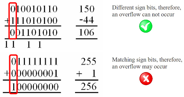
Figure 37 : Signed arithmetic overflow
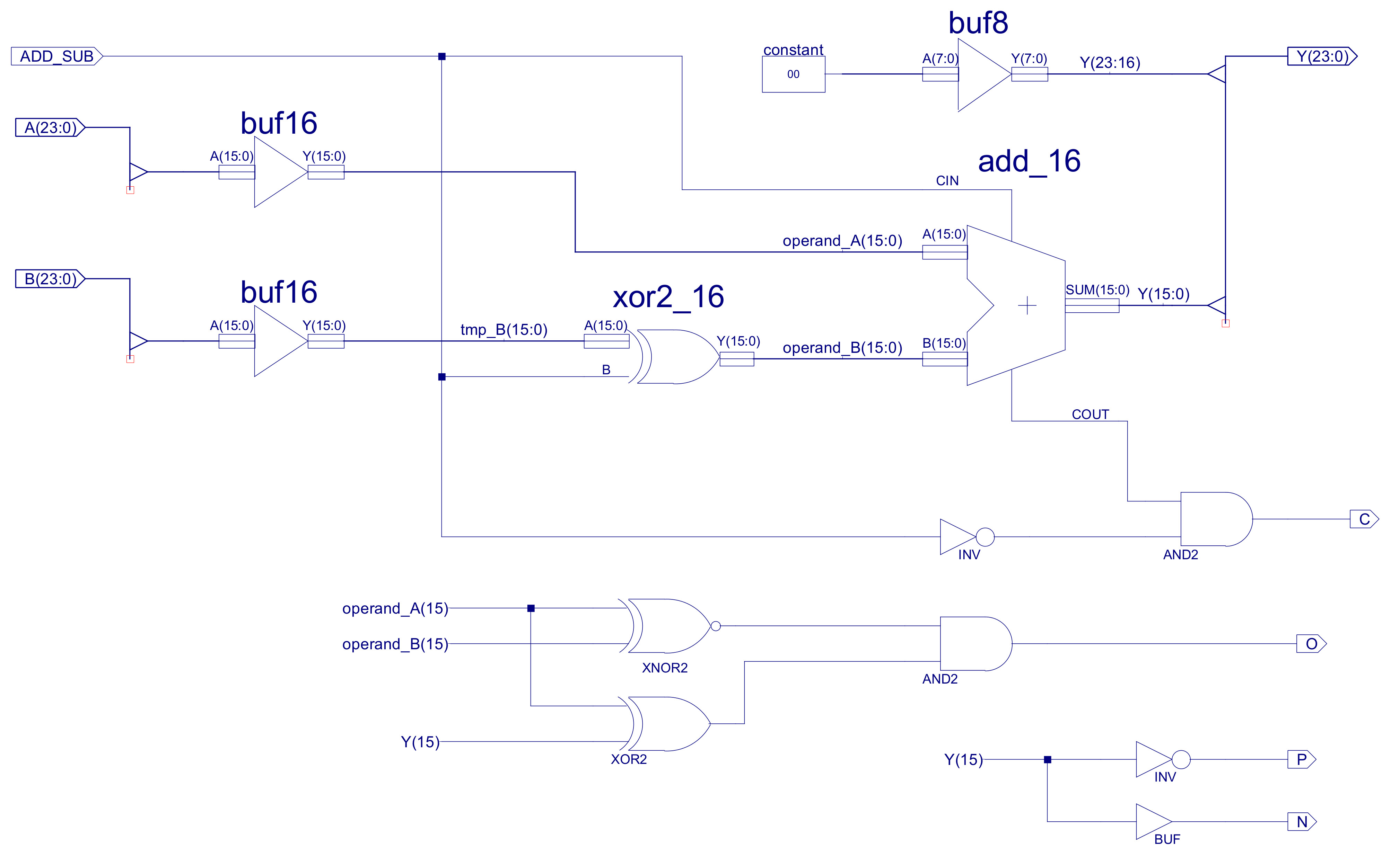
Figure 38 : Adder-subtractor
The O (overflow) status bit logic may be a bit tricky to understand, therefore, consider these 4bit examples:
  +7   0111     -7   1001     -7   1001     +7   0111     -8   1000
+ +1   0001   + +1   0001   + -1   1111   + -1   1111   + -1   1111
----   ----   ----   ----   ----   ----   ----   ----   ----   ----
  +8   1000     -6   1010     -8   1000     +6   0110     -9   0111

  overflow      ok            ok            ok            overflow
  C = 0         C = 0         C = 1         C = 1         C = 1
  O = 1         O = 0         O = 0         O = 0         O = 1

  +7   0111     -7   1001     -7   1001     +7   0111     -8   1000
- +1   0001   - +1   0001   - -1   1111   - -1   1111   - +1   0001
       1111          1111          0001          0001          1111
----   ----   ----   ----   ----   ----   ----   ----   ----   ----
  +6   0110     -8   1000     -6   1010     +8   1000     -9   0111

  ok            ok            ok            overflow      overflow
  C = 1         C = 1         C = 0         C = 0         C = 1
  O = 0         O = 0         O = 0         O = 1         O = 1
When using a four bit signed data type the largest positive number is +7, the largest negative number is -8. The MSB of the two operands are compared using the XNOR, producing a logic 1 when they are the same (XNOR and XOR truth tables shown below). If they are the same the MSB of the adder's output: Y15 is compared to the MSB of one of the operands: A15 (either would do) using an XOR gate. This output is set to a logic 1 if the result differs from the operand size bit i.e. rule 2 (listed above).
XNOR     XOR
A B Z    A B Z
0 0 1    0 0 0
0 1 0    0 1 1
1 0 0    1 0 1
1 1 1    1 1 0
The BITWISE_LOGIC component implements 24 bit bitwise AND, OR and XOR functions, as shown in figure 39. Structurally, the three bitwise functional blocks are identical, each performing the indicated logic function on each pair of input values e.g. for the bitwise_AND outputs will be Y0=A0&B0, Y1=A1&B1 etc. The internal construction of the bitwise_AND is shown in figures 40 and 41. The 24 individual AND gates are constructed from three AND2_8 components, to allow component reuse within the design. The bitwise_OR and bitwise_XOR, are implemented in exactly the same way, just replacing the AND gates shown in figure 41 with OR and XOR respectively.
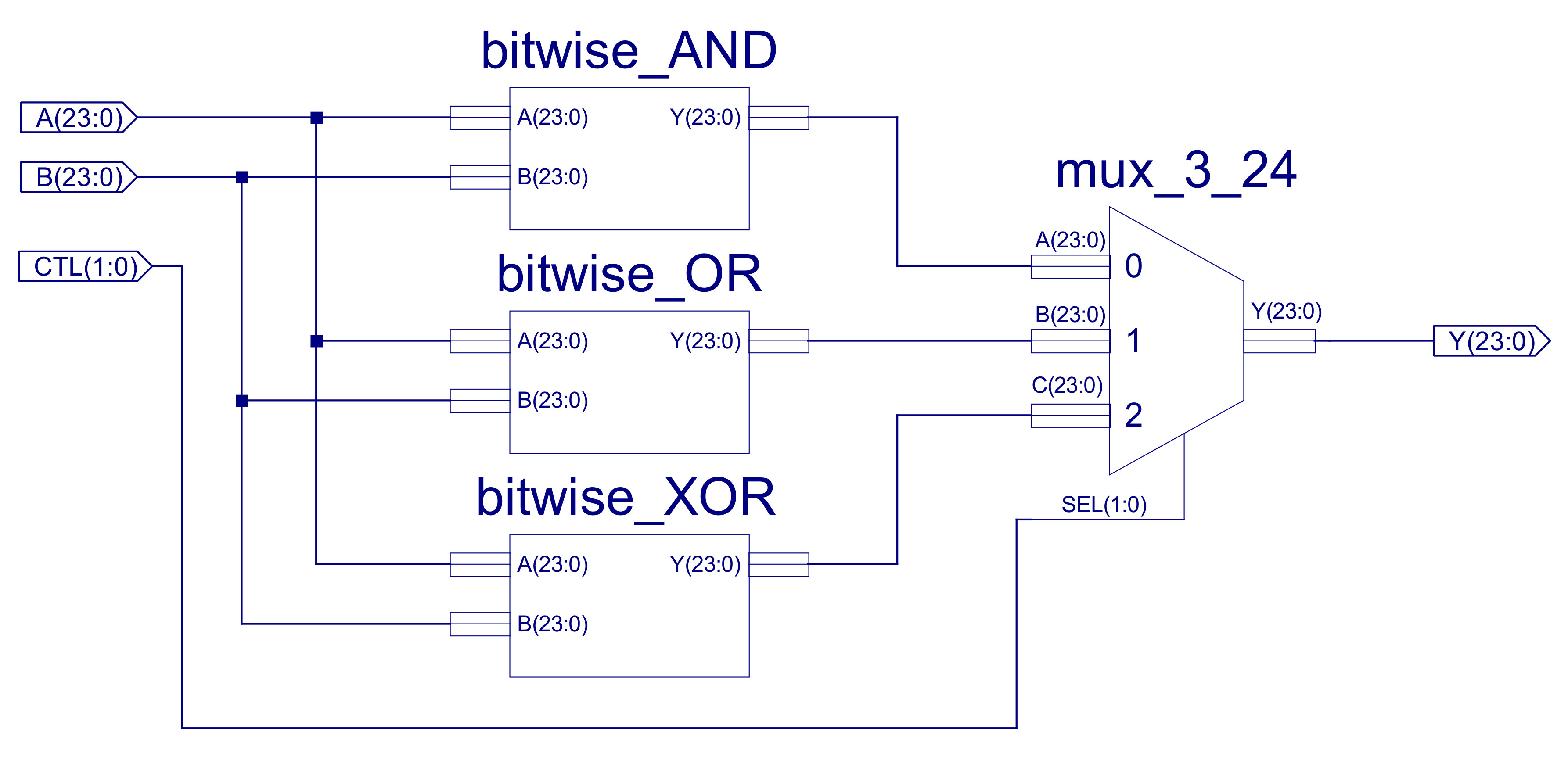
Figure 39 : Bitwise-Logic

Figure 40 : Bitwise-AND
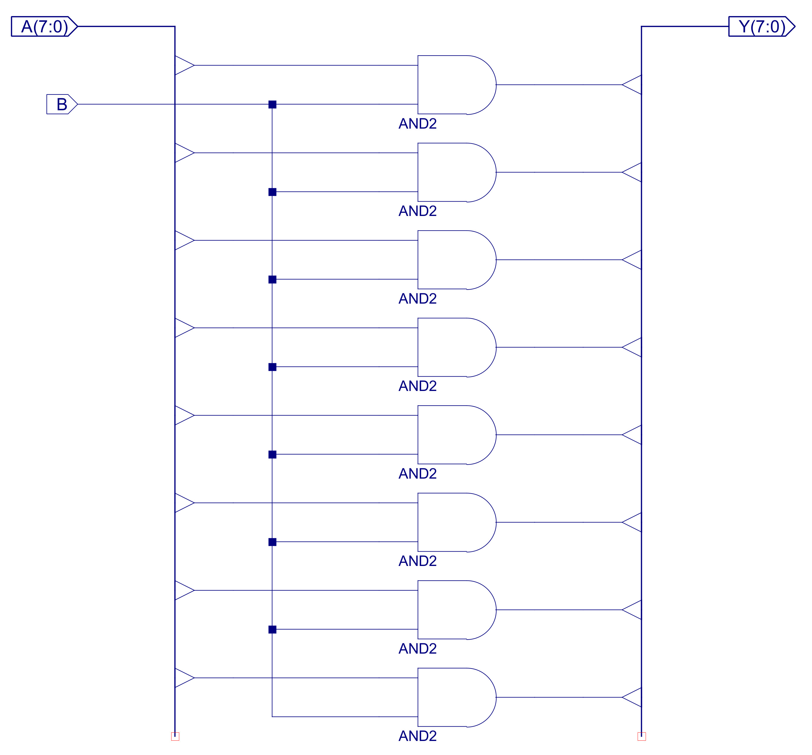
Figure 41 : AND2_8
The IMM16 component is used to zero the high byte of the B input of the ALU, as shown in figure 42. This component zeros the high byte of the 24 bit instruction to select the 16 bit immediate value. Note, could argue that this is not required, as the ADDER only uses the lower 16 bits i.e. bits 16 to 24 are ignored, but i decided to keep this in, to ensure registers where more human readable, and these results could be used later by functional units that do uses these high bits e.g. bitwise or shift instructions.
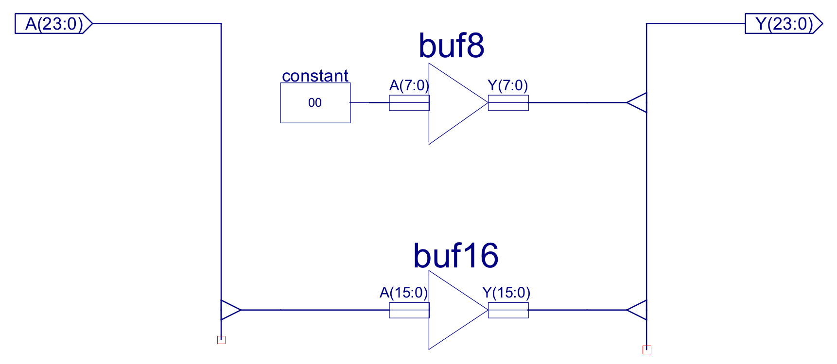
Figure 42 : IMM16 - 24bit to 16bit mask
The final functional units in this CPU are the SHIFT_ROTATE components as shown in figure 43. These are the simplest units in the ALU as you don't really need any logic gates, you only need wires. Each of these units shifts the input data one position to the left or the right, if the EN=0 the empty space is filled with a 0, if EN=1 the empty space is filled with the lost bit i.e. a rotate, as shown below:
               A3 A2 A1 A0      Y3 Y2 Y1 Y0      Value
Data value  :  0  1  0  1                          5

Shift right  :                  0  A3 A2 A1
                                0  0  1  0         2

Shift left  :                   A2 A1 A0 0
                                1  0  1  0         10

Data value  :  0  1  1  1                          7

Rotate right  :                 A0 A3 A2 A1
                                1  0  1  1         11

Rotate left :                   A2 A1 A0 0
                                1  1  1  0         14
The buffers shown in figure 43 are simply used to rewire the input bus (A) to the output bus (Y). In the above example this will be:
Figure 44 shows the implementation of the SHIFT_RIGHT component, the shift left component is structurally the same, just wired to shift bit value in the opposite direction. Although very simple these are useful functions for aligning data within a 24bit word, or performing multiplication (shift left) or division (shift right) by 2. Note, the difference between a shift and a rotate is that in a rotate you do not loose any bits, they are just recirculated around the register, whilst in shift the "space" created by the shift is filled with a 0 e.g. if you rotated a register 24 times you would get the same value, if you shifted a register 24 time you would zero the register. The unused bit in the shift operations is used to drive the COUT lines, at this time this is not used by the processor, but it could be combined with the C status bit from the ADDER-SUB. These are very simple fixed shifter units, you can also implement variable length shifts using additional multiplexer i.e. a Barrel shifter (Link).
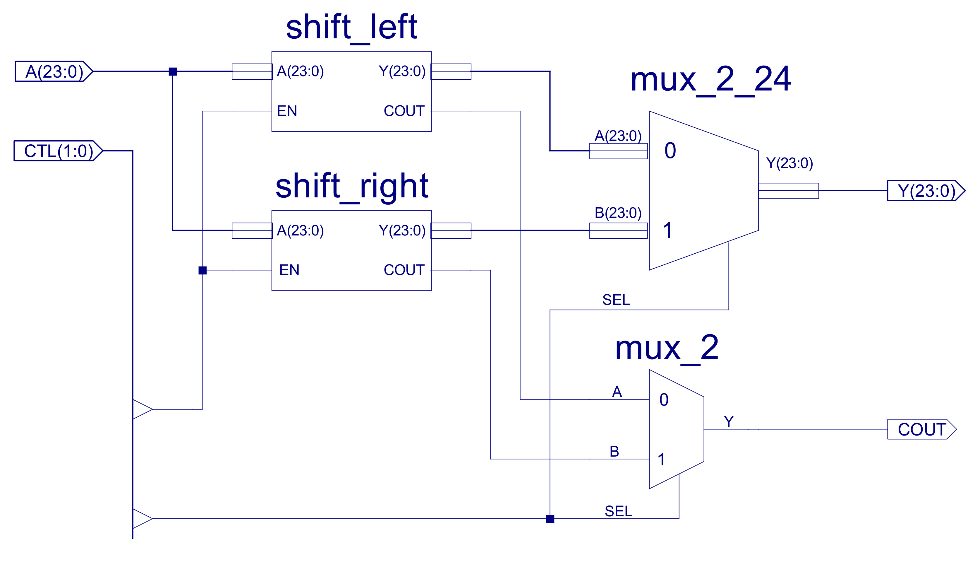
Figure 43 : Shift_Rotate component
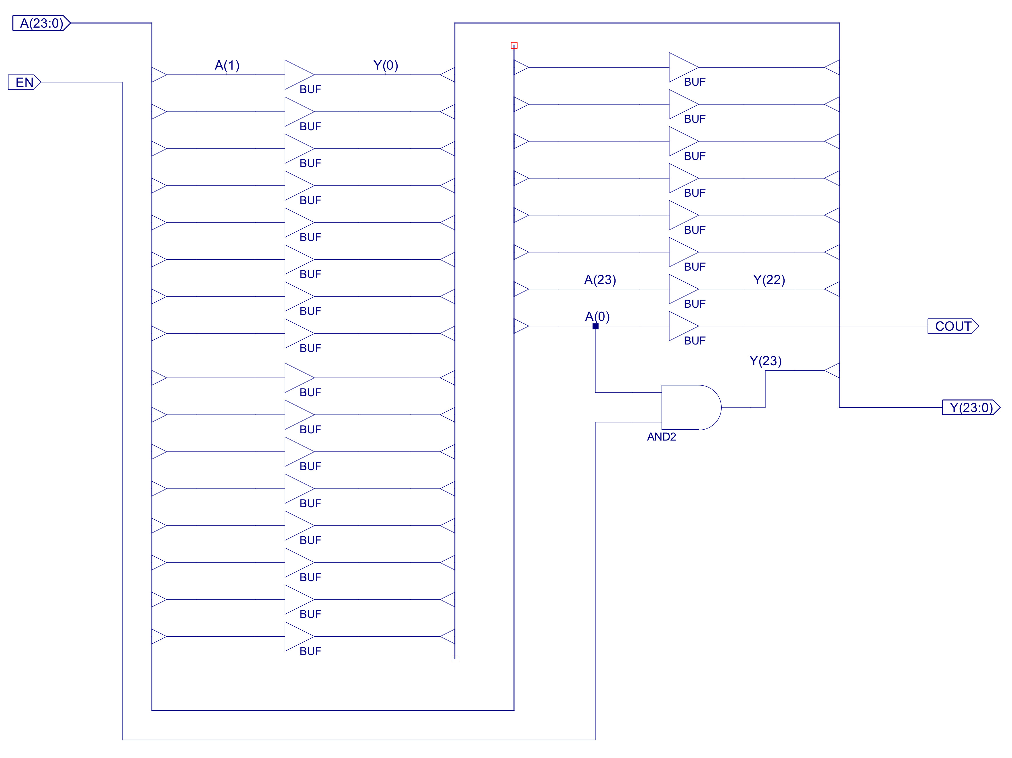
Figure 44 : Shift_Right component
At this time inputs 4 and 5 of the final MUX_8_24 output multiplexer are not used i.e. presently hardwired to 0x000000. It is intended that these will be used for application specific functional units later in the simpleCPU-v3's development. Input 6 and 7 are simple pass through's, allowing the ALU's A and B inputs to selected e.g. to pass through a value read from memory during a LOAD instruction, or when a register value is transferred into another register.
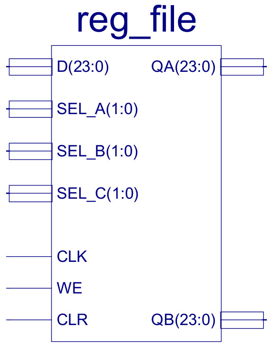
Figure 45 : Register file
The internal components of the register file are shown in figure 46. It contains four 24 bit registers, these being constructed from three 8 bit registers as shown in figure 47, these 8 bit registers are described here: (Link). Each register's D input is connected to the same D data bus, as only one result is produced by any instruction i.e. only one register is written to at any time. To select which register is updated one-hot decoder circuit shown in figure 48 is used, controlled by the SEL_C and WE signals. This logic only produces a logic 1 on one of its outputs (Y0, Y1, Y2 or Y3) when the WE input is pulsed high e.g. during a STORE instruction, otherwise these registers are not updated.

Figure 46 : Register file

Figure 47 : 24bit register
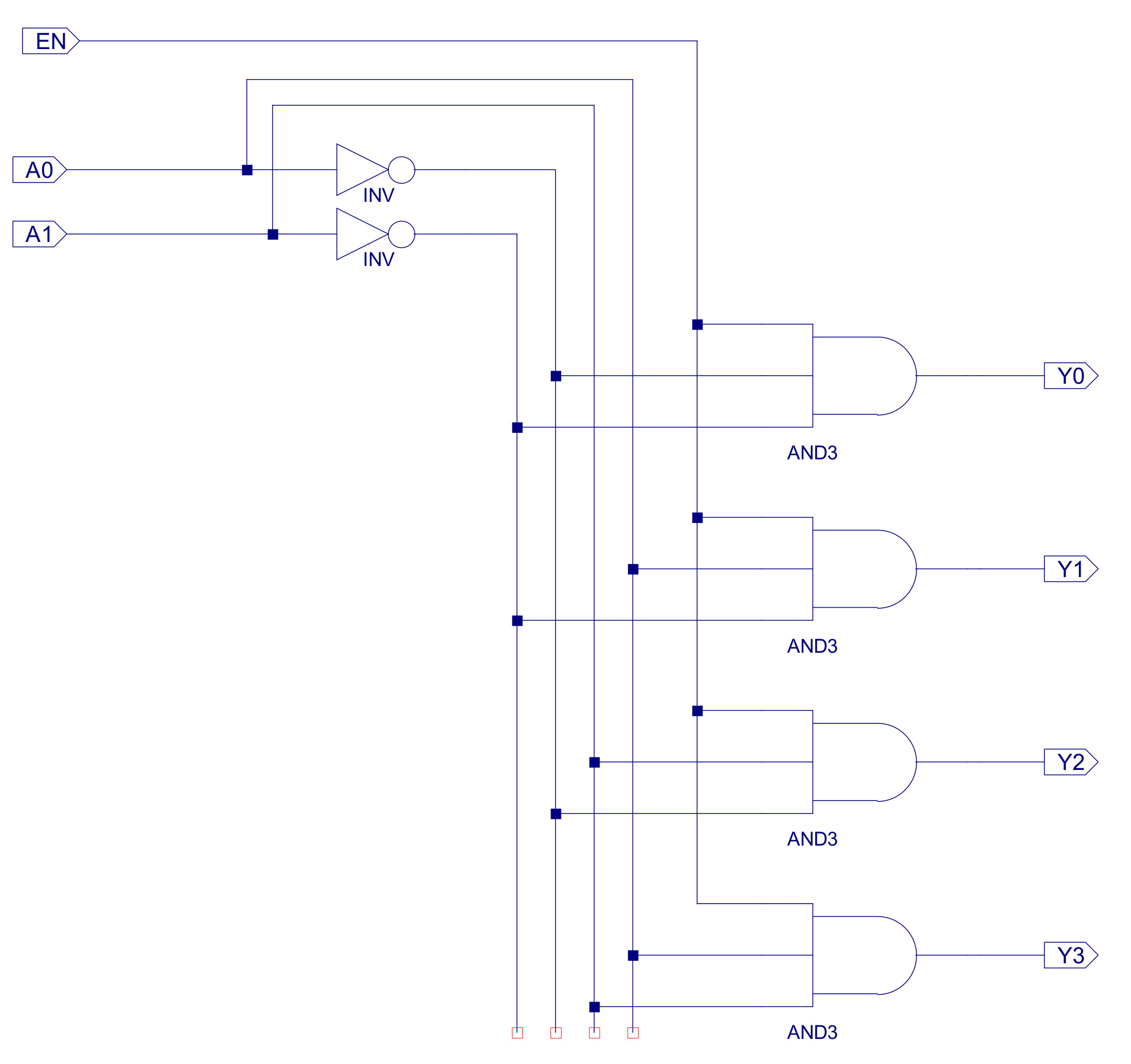
Figure 48 : One-hot decoder - register select logic
To support the new register addressing mode, the register file has two output ports: QA and QB, allowing an instruction to access any two of the four general purpose registers. These outputs are selected using the 24 bit x 4-input multiplexers, as shown in figure 35 (previously discussed). Note, this register file is said to have two read ports and one write port. Processors that need to access more operands in the same clock cycle would have to increase the size of these ports i.e. add more multiplexers. If a processor has an instruction that produces four results e.g. the instructions shown in figure 1, we would need a register file that has eight read ports and four write ports, which significantly adds to hardware size and complexity.
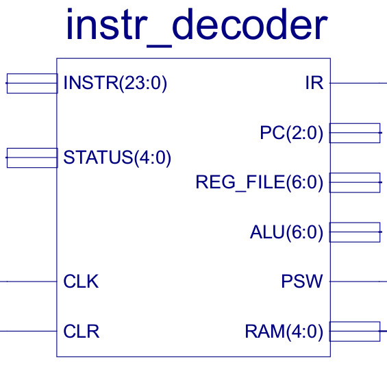
Figure 49 : Decoder - control logic
To help structure the decoder's logic i sub-divided the 6 bit opcode field, giving each "addressing mode" an unique 2 bit code, assigning this to the first two bits of each instruction i.e MSB and MSB-1:
Therefore, by simply looking at the top two bits you can identify the type of instruction and its addressing mode, well sort of, it one way of grouping the instructions based on the bit fields used in the instruction. This is perhaps not the most efficient way of designing the CPU's machine code representation for each instruction i.e. i'm sure the number of bits used to represent each instruction and the amount of logic used to decode then could of been reduced, but hopefully this approach gives the decoder a little more structure. The lower 4 bits of the 6 bit opcode is used to identify each instruction that uses that addressing mode. The top level schematic of the decoder is shown in figure 50. This is very similar to the previous simpleCPUv1's design, we still have the 3 bit ring counter, generating the Fetch, Decode and Execute phase signals. There is also a 4bit to 16bit one-hot decoder that processes each instructions opcode. However, in addition to these i've added a 2 bit to 4 bit one-hot decoder (same as that shown in figure 48), that decodes the top two bits of the instruction i.e. the addressing mode. These signals are only active during the Decode and Execute phases, enabling only that logic associated with the addressing mode being performed.
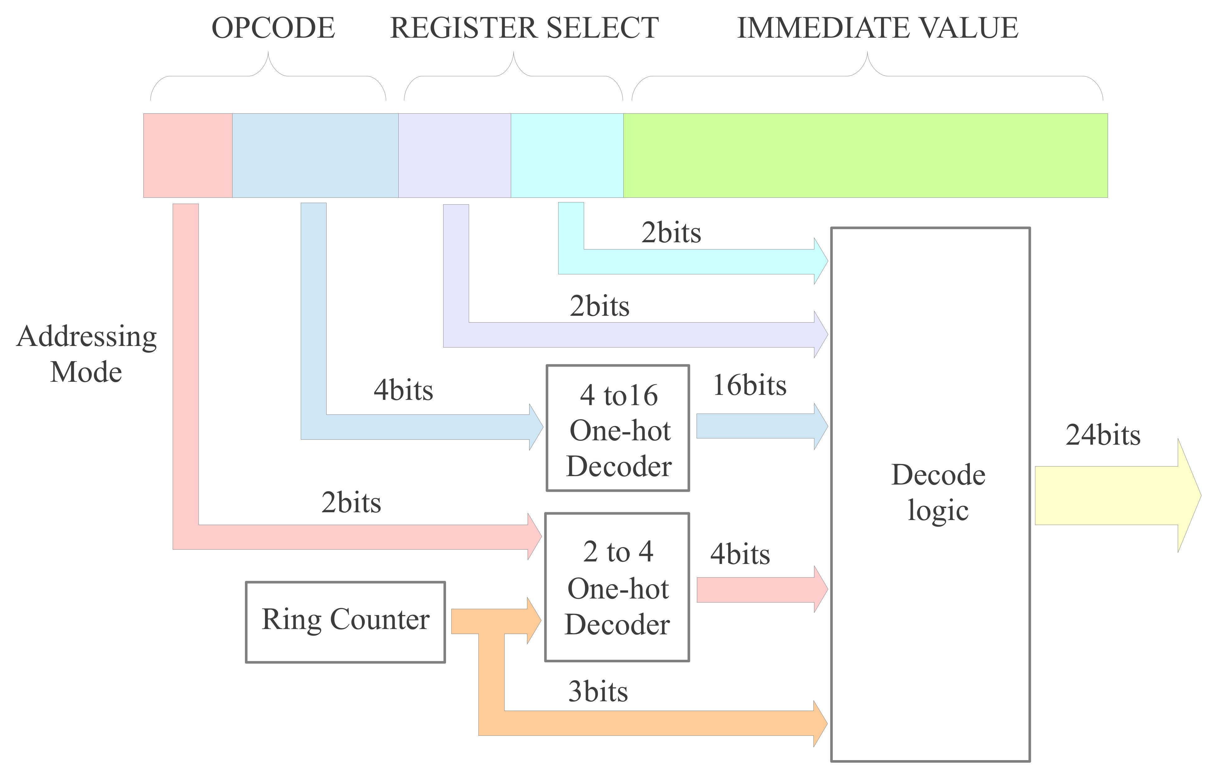
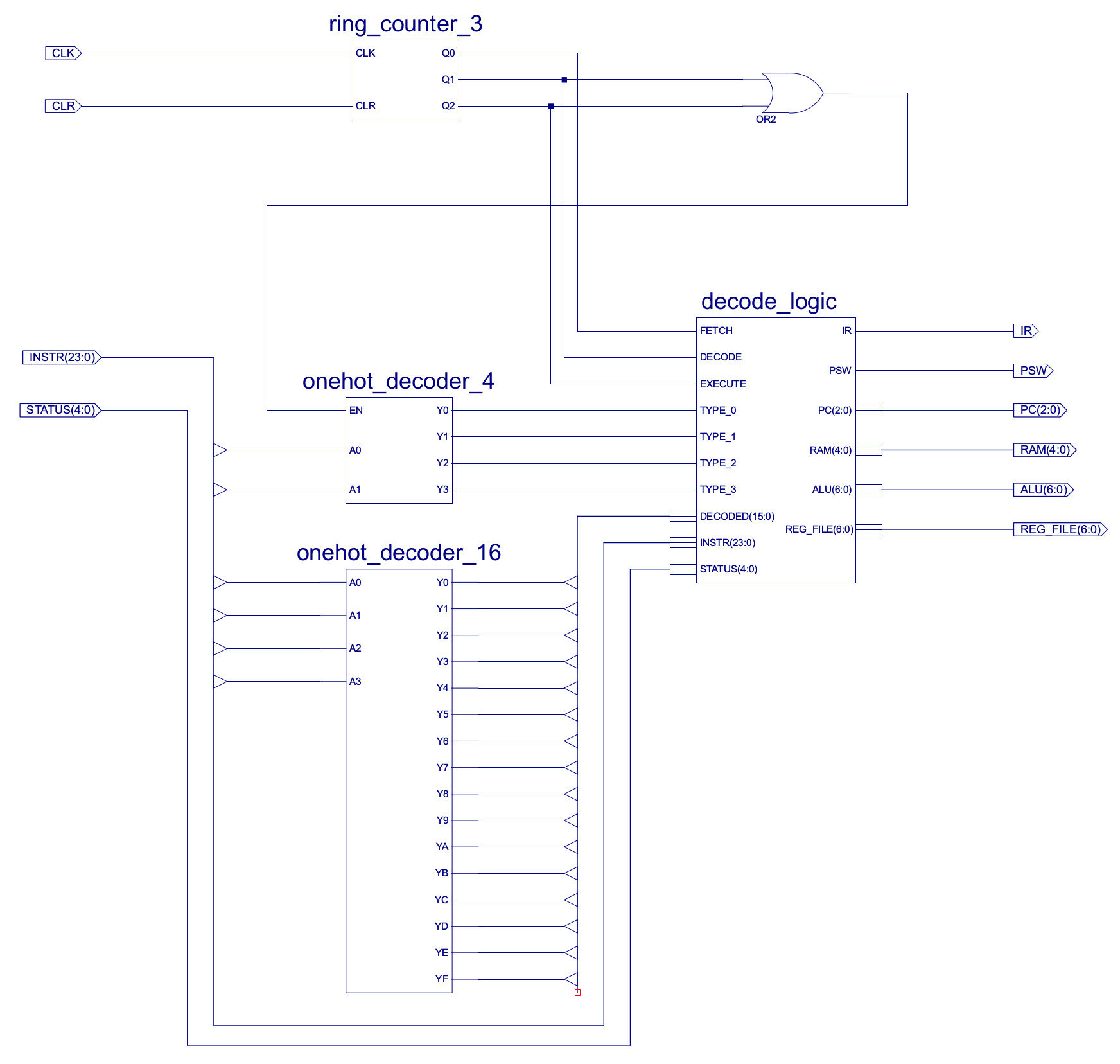
Figure 50 : instruction decoder, block diagram (top), schematic (bottom)
The DECODE_LOGIC component uses these one-hot values, the processor's status word (Z,C,O,P,N) and bit fields within the instruction register (IR) to generate the sequence of control signals needed to implement each instruction. The top level schematic of the logic circuit used to generate these signals is shown in figure 51.
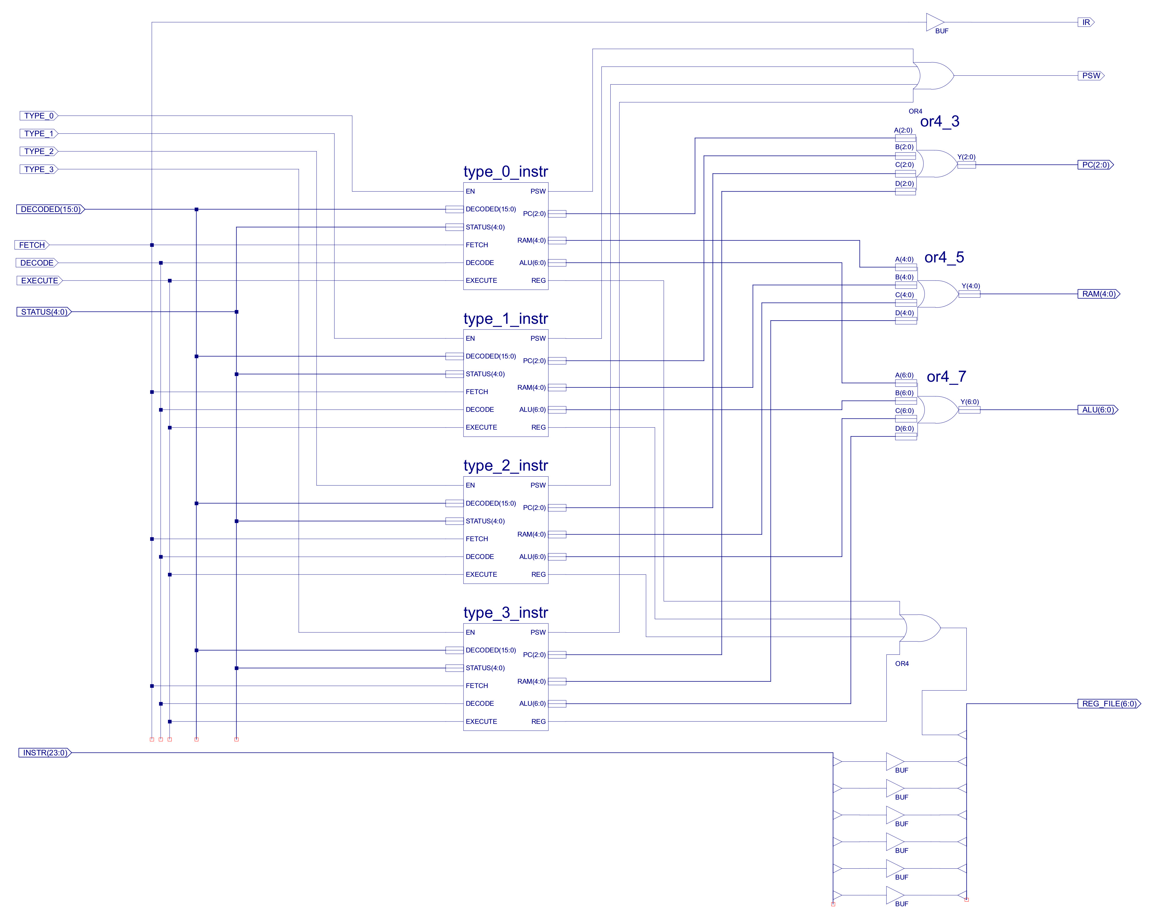
Figure 51 : instruction decoder
Each instruction type i.e. based on addressing mode (type-0, type-1, type-2 and type-3), is decoded by a separate logic block. These blocks having identical input and output pins:
Only one block is active at any time, being selected by the top two bits of the instruction being decoded i.e. the control signals: type_0, type_1, type_2 and type_3, driven by the 2-to-4 one-hot decoder (only ever one logic 1). When the EN line of a decoder block is 0, that block is disabled, setting all of its outputs to 0 i.e. the only block that can set its outputs to a logical 1 is the active block i.e. the block where EN=1. OR gates are then used to connect each block's output signals to the associated control signals within the processor e.g. the program counter control lines PC(2:0) from each of the four blocks are connected together using the component OR4_3, as shown in figure 52.
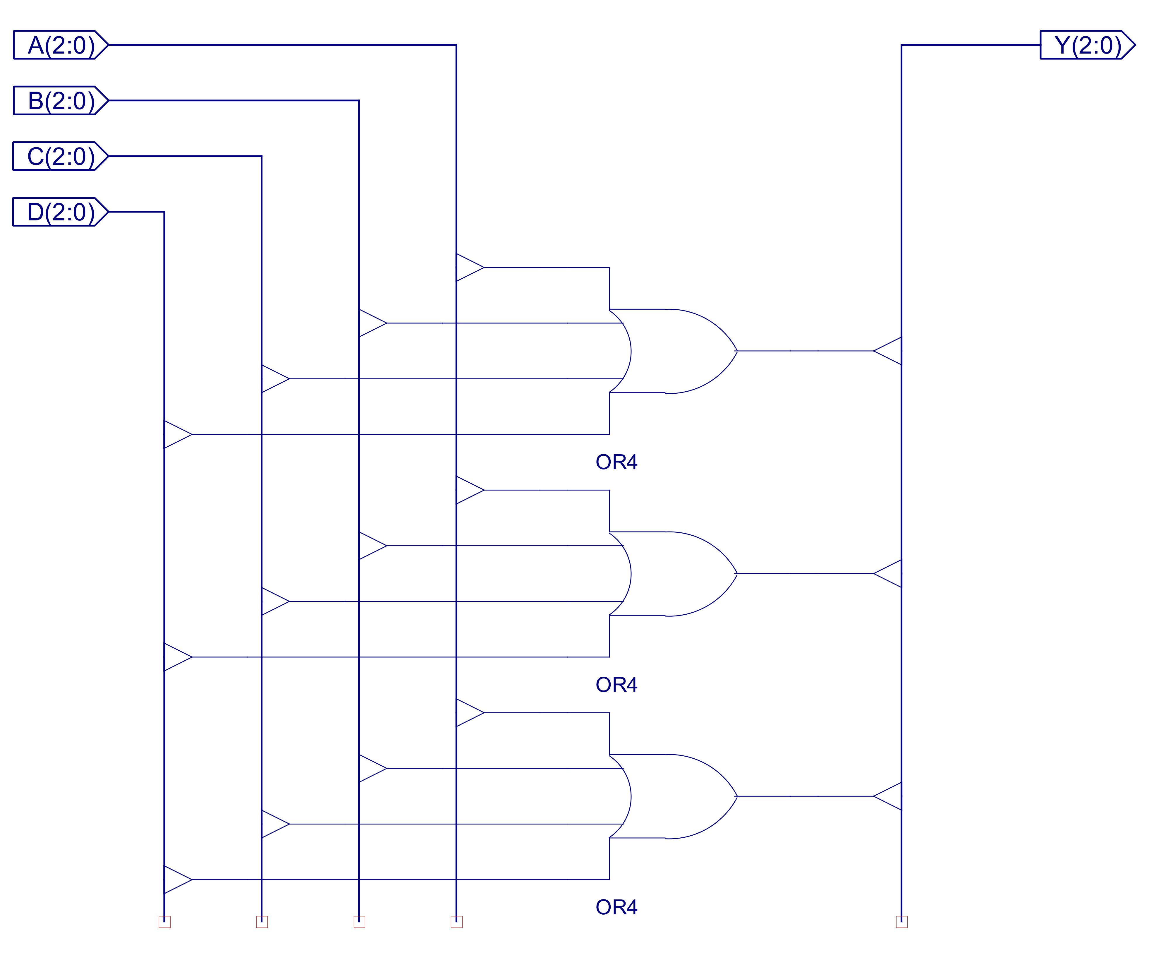
Figure 52 : OR4_3 component
Each bit position of the four 3 bit output busses are logical ORed together to produce the final control signal e.g. Y0 = A0 OR B0 OR C0 OR D0 etc. As only one decoder block is active at any time, the inactive blocks will be be remove, as their outputs will be set to 0 e.g. if the instruction is type-0 only input A is active, therefore, Y0 = A0 OR 0 OR 0 OR 0 = A0. This is repeated for each of the output pins. Note, one of the advantages of this approach is that you can easily add new instructions, or remove old ones without having to modify the other decoder blocks.Again, as with the simpleCPU v1a decoder (Link) decode logic generation is simply the process of mapping the identified logic 1 states identified in the control logic truth table into simple logic circuits contracted form: OR, AND or CONSTANTs. Note, there are lots of different ways of doing this, you just need to ensure that when the input EN=0, all outputs are set to 0. Note, the only exceptions to this rule are the IR and RAM enable signals, as these are identical in all decode blocks e.g. we always want to enable the RAM. Below is a quick discussion of how the logic for type-0 instructions was designed, as shown in figure 53.

Figure 53 : Type-0 instruction decoder
At this time the simpleCPUv3 supports the following instruction set:
Instruction          :          Bit positions          :         RTL              :       Example
Move  Rx     0xdddd  :  00 0000 XX DD DDDDDD DDDDDDDD  :  Rx <- 0xdddd            :  move  Ra, 0x1234
Add   Rx     0xdddd  :  00 0001 XX DD DDDDDD DDDDDDDD  :  Rx <- Rx + 0xdddd       :  add   Ra, 0x1234
Sub   Rx     0xdddd  :  00 0010 XX DD DDDDDD DDDDDDDD  :  Rx <- Rx - 0xdddd       :  sub   Ra, 0x1234
Load  Rx     0xdddd  :  00 0011 XX AA AAAAAA AAAAAAAA  :  Rx <- M[0xaaaa]         :  load  Ra, 0x1234
Store Rx     0xdddd  :  00 0100 XX AA AAAAAA AAAAAAAA  :  M[0xaaaa] <- Rx         :  store Ra, 0x1234
And   Rx     0xdddd  :  00 0101 XX DD DDDDDD DDDDDDDD  :  Rx <- Rx & 0xdddd       :  and   Ra, 0x1234
Or    Rx     0xdddd  :  00 0110 XX DD DDDDDD DDDDDDDD  :  Rx <- Rx | 0xdddd       :  or    Ra, 0x1234
Xor   Rx     0xdddd  :  00 0111 XX DD DDDDDD DDDDDDDD  :  Rx <- Rx ^ 0xdddd       :  Xor   Ra, 0x1234

Move  Rx Ry          :  01 0000 XX YY ...... ........  :  Rx <- Ry                :  move  Ra,  Rb
Add   Rx Ry          :  01 0001 XX YY ...... ........  :  Rx <- Rx + Ry           :  add   Ra,  Rb
Sub   Rx Ry          :  01 0010 XX YY ...... ........  :  Rx <- Rx - Ry           :  sub   Ra,  Rb
Load  Rx (Ry)        :  01 0011 XX YY ...... ........  :  Rx <- M[Ry]             :  load  Ra, (Rb)
Store Rx (Ry)        :  01 0100 XX YY ...... ........  :  M[Ry] <- Rx             :  store Ra, (Rb)
And   Rx Ry          :  01 0101 XX YY ...... ........  :  Rx <- Rx & Ry           :  and   Ra,  Rb
Or    Rx Ry          :  01 0110 XX YY ...... ........  :  Rx <- Rx | Ry           :  or    Ra,  Rb
Xor   Rx Ry          :  01 0111 XX YY ...... ........  :  Rx <- Rx ^ Ry           :  xor   Ra,  Rb
Sr0   Rx             :  01 1000 XX .. ...... ........  :  Rx <- Rx >> 1           :  sr0 Ra
Sl0   Rx             :  01 1001 XX .. ...... ........  :  Rx <- Rx << 1           :  sl0 Ra
Ror   Rx             :  01 1010 XX .. ...... ........  :  Rx <- Rx >> 1           :  ror Ra
Rol   Rx             :  01 1011 XX .. ...... ........  :  Rx <- Rx << 1           :  rol Ra

Jump  U      0xaaaa  :  10 0000 .. AA AAAAAA AAAAAAAA  :  PC <- 0xaaaa            : jumpU 0x1234
Jump  Z      0xaaaa  :  10 0001 .. AA AAAAAA AAAAAAAA  :  if Z:  PC <- 0xaaaa     : jumpZ 0x1234
Jump  NZ     0xaaaa  :  10 0010 .. AA AAAAAA AAAAAAAA  :  if NZ: PC <- 0xaaaa     : jumpNZ 0x1234
Jump  C      0xaaaa  :  10 0011 .. AA AAAAAA AAAAAAAA  :  if C:  PC <- 0xaaaa     : jumpC 0x1234
Jump  NC     0xaaaa  :  10 0100 .. AA AAAAAA AAAAAAAA  :  if NC: PC <- 0xaaaa     : jumpNC 0x1234
Jump  N      0xaaaa  :  10 0101 .. AA AAAAAA AAAAAAAA  :  if N:  PC <- 0xaaaa     : jumpN 0x1234
Jump  NN     0xaaaa  :  10 0110 .. AA AAAAAA AAAAAAAA  :  if NN: PC <- 0xaaaa     : jumpNN 0x1234
Jump  P      0xaaaa  :  10 0111 .. AA AAAAAA AAAAAAAA  :  if P:  PC <- 0xaaaa     : jumpP 0x1234
Jump  NP     0xaaaa  :  10 1000 .. AA AAAAAA AAAAAAAA  :  if NP: PC <- 0xaaaa     : jumpNP 0x1234
Jump  O      0xaaaa  :  10 1001 .. AA AAAAAA AAAAAAAA  :  if O:  PC <- 0xaaaa     : jumpO 0x1234
Jump  NO     0xaaaa  :  10 1010 .. AA AAAAAA AAAAAAAA  :  if NO: PC <- 0xaaaa     : jumpNO 0x1234

Jump  (Ry)           :  10 1011 .. YY ...... ........  :  PC <- Ry                : jump (Ra)
Call         0xaaaa  :  10 1100 .. .. AAAAAA AAAAAAAA  :  PC <- 0xaaaa, Rd <- PC  : call 0x1234
Ret                  :  10 1101 .. .. ...... ........  :  PC <- Rd                : ret

Dump                 :  11 1111 .. .. ...... ........  :  DMP <- 1                : dump
Key: "." = not used, "D" = data bit, "A" = address bit, "X" = register X select bit, "Y" = register Y select bit. Register RX and RY can be any of the four general purpose registers i.e. RA, Rb, RC, or RD. Addresses and immediate data values are limited to 16 bit values. All instructions are 24 bit fixed length.
There are 33 instructions, but this could be expanded to 64 if needed. From the image processing point of view we could definitely implement some RGB specific instructions e.g. SIMD type instructions, processing the three 8 bit values in one instruction. However, for the moment we have the basics. Note, the CALL instruction is a modified JUMP, when this instruction is executed the current value of the PC (already incremented by 1) is stored in register RD. If this register is needed by the subroutine, it is responsible for buffering this value out to external memory, or a software implemented stack in external memory. If a software stack is implemented in memory you would also need to consider using one of the general purpose registers as a stack pointer. This approach is quite common in RISCs e.g. you may typically "have" 32 general purpose registers in these machines, but you soon find out that some are reserved for other purposes, which quickly reduces the number of true general purpose registers available to the programmer :). The DUMP instruction is only really used in simulations, if this instruction is executed the CPU pulses the DMP input on the memory component, dumping its current state to a file on the host computer running the simulation.
The next step is to write out the truth table defining the state of each control signal during each instruction phase. This is written out in a spreadsheet which can be accessed here: (Link), each row defines a micro-instruction used to implement the above machine-instructions i.e. the state of the processor's control signals for each phase of the instruction (FDE) is a micro-instruction. This table is a little large to fit on one screen, so ive cut and pasted just the type-0 instructions into figure 54. To show how these are now implemented in logic consider the register-file's WE signal, labelled REG(6) in figure 54. If you look at this signal it is set to a logic 1 during the execute phase for all of the instructions except the STORE instruction (instruction opcode 4), as this writes data to memory rather than the register file. Therefore, the logic to implement this column is simply that shown in figure 55 (also shown in the bottom of figure 53).
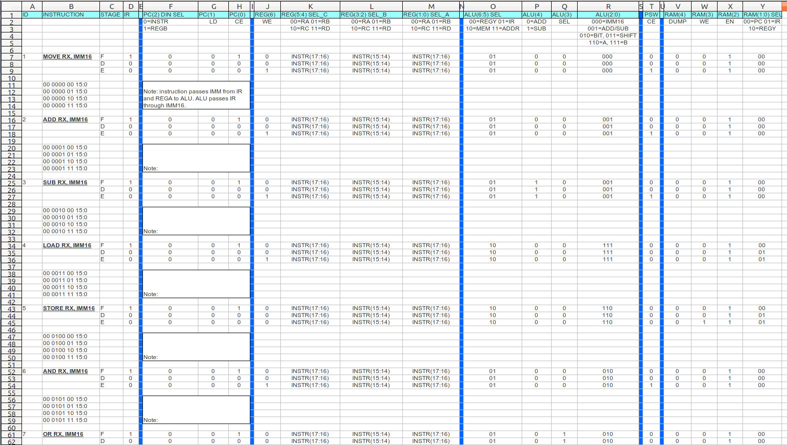
Figure 54 : Type-0 micro-instructions
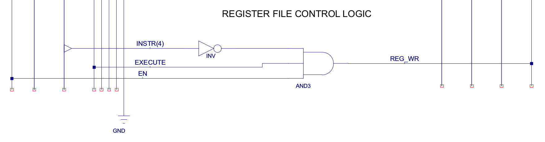
Figure 55 : Type-0 micro-instructions - REG control logic
Figure 56 : simpleCPU v3 schematic
The top level schematic for the simpleCPU v3 is shown in figure 56, there are a few extra components not already discussed. IMM24 shown in figure 57, converts the 16 bit PC into a 24 bit value so that it can be connected to the ALU's data multiplexer i.e. setting the top byte to zero. The processor's status word is implemented using the component REG_5, a simple 5 bit registers, as shown in figure 58. The CPU's address bus is controlled using the MUX_3_16 component, a three-input 16 bit multiplexer, as shown in figure 59. As always you hope you have implemented the hardware correctly, the only way to test it is to run that test code :).
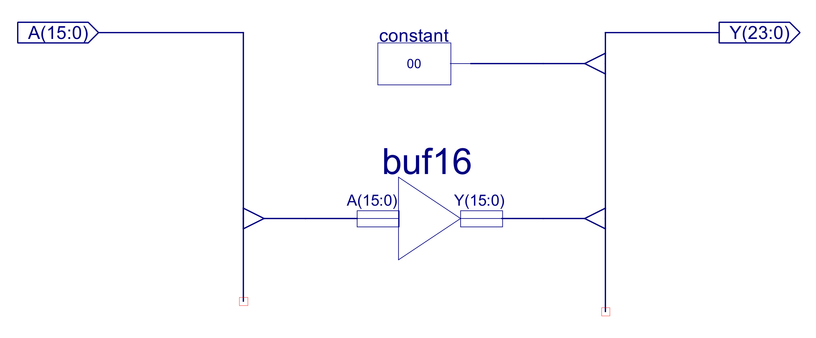
Figure 57 : IMM24 - 16 bit to 24 bit bus extender
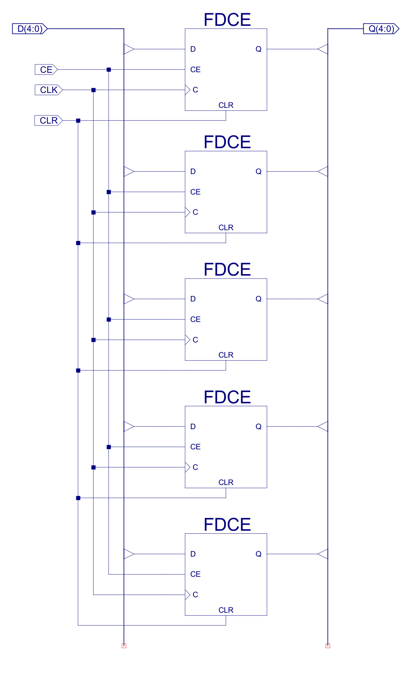
Figure 58 : REG_5 - processor's status word

Figure 59 : 16bit x 3-input multiplexer
The first test program is shown below, testing type-0 instructions. A simulation of the processor executing this code is shown in figure 60, this is split into two sections, each approximately 13us long, total simulation time 23us. At first glance this is just a sea of squiggles, but if you look at how the registers are changing you can clearly see each block in the program being executed. Between approximately:
The final memory dump file can be accessed here: (Link). If you scroll through this file you can see that data has been stored at address 64 (0x40). Note, when counting lines to calculate the address remember to start at 0 and remove the header block.
#
# MOVE : RA=1, RB=2, RC=3, RD=4
#
00 00 0000 00 00000000 00000001
01 00 0000 01 00000000 00000010
02 00 0000 10 00000000 00000011
03 00 0000 11 00000000 00000100
#
# ADD : RA=1+2, RB=2+2, RC=3+2, RD=4+2
#
04 00 0001 00 00000000 00000010
05 00 0001 01 00000000 00000010
06 00 0001 10 00000000 00000010
07 00 0001 11 00000000 00000010
#
# SUB : RA=3-1, RB=4-1, RC=5-1, RD=6-1
#
08 00 0010 00 00000000 00000001
09 00 0010 01 00000000 00000001
10 00 0010 10 00000000 00000001
11 00 0010 11 00000000 00000001
#
# STORE : M[0x40]=RA, M[0x41]=RB, M[0x42]=RC, M[0x43]=RD
#
12 00 0100 00 00000000 01000000
13 00 0100 01 00000000 01000001
14 00 0100 10 00000000 01000010
15 00 0100 11 00000000 01000011
#
# LOAD : RA=M[0x43], RB=M[0x42], RC=M[0x41], RD=M[0x40]
#
16 00 0011 11 00000000 01000000
17 00 0011 10 00000000 01000001
18 00 0011 01 00000000 01000010
19 00 0011 00 00000000 01000011
#
# OR : RA=RA|0xFF00, RB=RB|0xFF00, RC=RC|0xFF00, RD=RD|0xFF00
#
20 00 0110 00 11111111 00000000
21 00 0110 01 11111111 00000000
22 00 0110 10 11111111 00000000
23 00 0110 11 11111111 00000000
#
# AND : RA=RA&0xF000, RB=RB&0xF000, RC=RC&0xF000, RD=RD&0xF000
#
24 00 0101 00 11110000 00000000
25 00 0101 01 11110000 00000000
26 00 0101 10 11110000 00000000
27 00 0101 11 11110000 00000000
#
# XOR : RA=RA^0xFFFF, RB=RB^0xFFFF, RC=RC^0xFFFF, RD=RD^0xFFFF
#
28 00 0111 00 11111111 11111111
29 00 0111 01 11111111 11111111
30 00 0111 10 11111111 11111111
31 00 0111 11 11111111 11111111
#
# DUMP :
#
32 11 1111 11 11 11111111111111
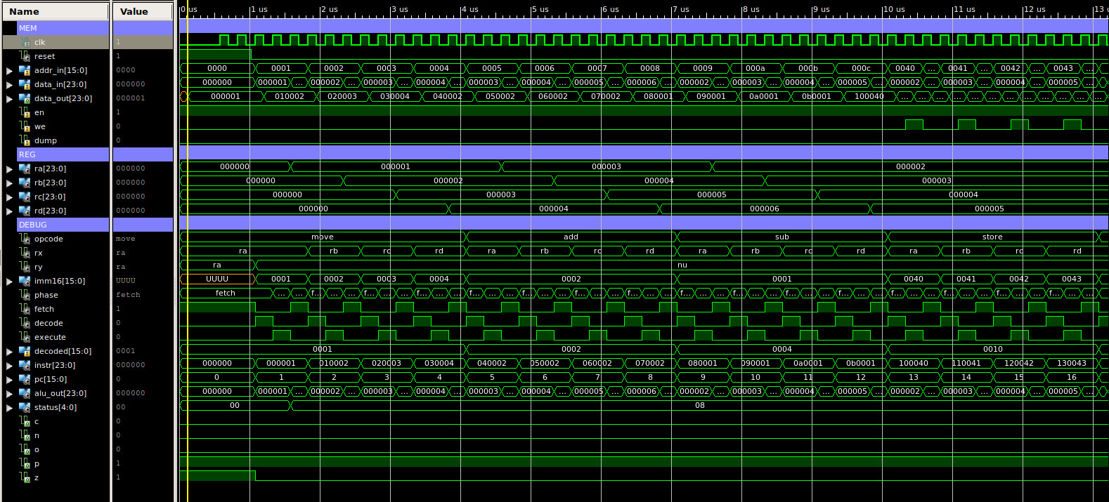
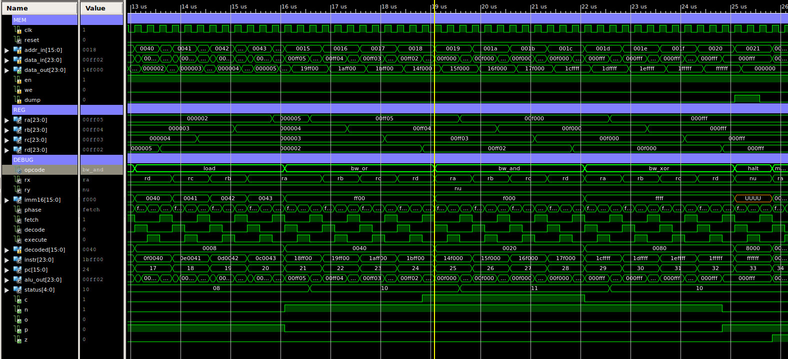
Figure 60 : type-0 instructions simulation
The next test program focuses on register addressing modes, testing type-1 instructions, as shown below. A simulation of the processor executing this code is shown in figure 61, this is split into four sections, each approximately 13us long, total simulation time 44us. Again, at first glance we have our normal sea of squiggles, but, between approximately:
The final memory dump file can be accessed here: (Link). If you scroll through this file you can see that data has been stored at address 64 (0x40). Note, when counting lines to calculate the address remember to start at 0 and remove the header block.
#
# MOVE : RA=1, RA=RA, RB=RA, RC=RA, RD=RA
#
00 00 0000 00 00000000 00000001
01 01 0000 00 00 00000000000000
02 01 0000 01 00 00000000000000
03 01 0000 10 00 00000000000000
04 01 0000 11 00 00000000000000
#
# MOVE : RB=2, RA=RB, RB=RB, RC=RB, RD=RB
#
05 00 0000 01 00000000 00000010
06 01 0000 00 01 00000000000000
07 01 0000 01 01 00000000000000
08 01 0000 10 01 00000000000000
09 01 0000 11 01 00000000000000
#
# MOVE : RC=3, RA=RC, RB=RC, RC=RC, RD=RC
#
10 00 0000 10 00000000 00000011
11 01 0000 00 10 00000000000000
12 01 0000 01 10 00000000000000
13 01 0000 10 10 00000000000000
14 01 0000 11 10 00000000000000
#
# MOVE : RD=4, RA=RD, RB=RD, RC=RD, RD=RD
#
15 00 0000 11 00000000 00000100
16 01 0000 00 11 00000000000000
17 01 0000 01 11 00000000000000
18 01 0000 10 11 00000000000000
19 01 0000 11 11 00000000000000
#
# ADD : RA=RA+RB, RB=RB+RA, RC=RC+RB, RD=RD+RC
#
20 01 0001 00 01 00000000000000
21 01 0001 01 00 00000000000000
22 01 0001 10 01 00000000000000
23 01 0001 11 10 00000000000000
#
# STORE : RD=0x40, M[0x80]=RA, M[0x81]=RB, M[0x82]=RC
#                  RD=RD+1,    RD=RD+1
#
24 00 0000 11 00000000 10000000
25 01 0100 00 11 00000000000000
26 00 0001 11 00000000 00000001
27 01 0100 01 11 00000000000000
28 00 0001 11 00000000 00000001
29 01 0100 10 11 00000000000000
#
# LOAD : RD=0x42, M[0x82]=RA, M[0x81]=RC, M[0x80]=RB
#                  RD=RD-1,    RD=RD-1
#
30 01 0011 00 11 00000000000000
31 00 0010 11 00000000 00000001
32 01 0011 10 11 00000000000000
33 00 0010 11 00000000 00000001
34 01 0011 01 11 00000000000000
#
# SUB : RD=RD-RC, RC=RC-RB, RB=RB-RA, RA=RA-RD
#
35 01 0010 11 10 00000000000000
36 01 0010 10 01 00000000000000
37 01 0010 01 00 00000000000000
38 01 0010 00 11 00000000000000
#
# OR : RD=0xFF, RA=RA|RD, RB=RB|RD, RC=RC|RD, RD=RD|RD
#
39 00 0000 11 00000000 11111111
40 01 0110 00 11 00000000000000
41 01 0110 01 11 00000000000000
42 01 0110 10 11 00000000000000
43 01 0110 11 11 00000000000000
#
# AND : RD=0x0F, RA=RA&RD, RB=RB&RD, RC=RC&RD, RD=RD&RD
#
44 00 0000 11 00000000 00001111
45 01 0101 00 11 00000000000000
46 01 0101 01 11 00000000000000
47 01 0101 10 11 00000000000000
48 01 0101 11 11 00000000000000
#
# XOR : RD=0xFF, RA=RA^RD, RB=RB^RD, RC=RC^RD, RD=RD^RD
#
49 00 0000 11 00000000 11111111
50 01 0111 00 11 00000000000000
51 01 0111 01 11 00000000000000
52 01 0111 10 11 00000000000000
53 01 0111 11 11 00000000000000
#
# SR0 : RA>>1, RB>>1, RC>>1, RD>>1
#
54 01 1000 00 00000000 00000000
55 01 1000 01 00000000 00000000
56 01 1000 10 00000000 00000000
57 01 1000 11 00000000 00000000
#
# SL0 : RA<<1, RB<<1, RC<<1, RD<<1,
#
58 01 1001 00 00000000 00000000
59 01 1001 01 00000000 00000000
60 01 1001 10 00000000 00000000
61 01 1001 11 00000000 00000000
#
# ROR : RA>>1, RB>>1, RC>>1, RD>>1
#
62 01 1010 00 00000000 00000000
63 01 1010 01 00000000 00000000
64 01 1010 10 00000000 00000000
65 01 1010 11 00000000 00000000
#
# ROL : RA<<1, RB<<1, RC<<1, RD<<1,
#
66 01 1011 00 00000000 00000000
67 01 1011 01 00000000 00000000
68 01 1011 10 00000000 00000000
69 01 1011 11 00000000 00000000
#
# DMP :
#
70 11 1111 11 11111111 11111111
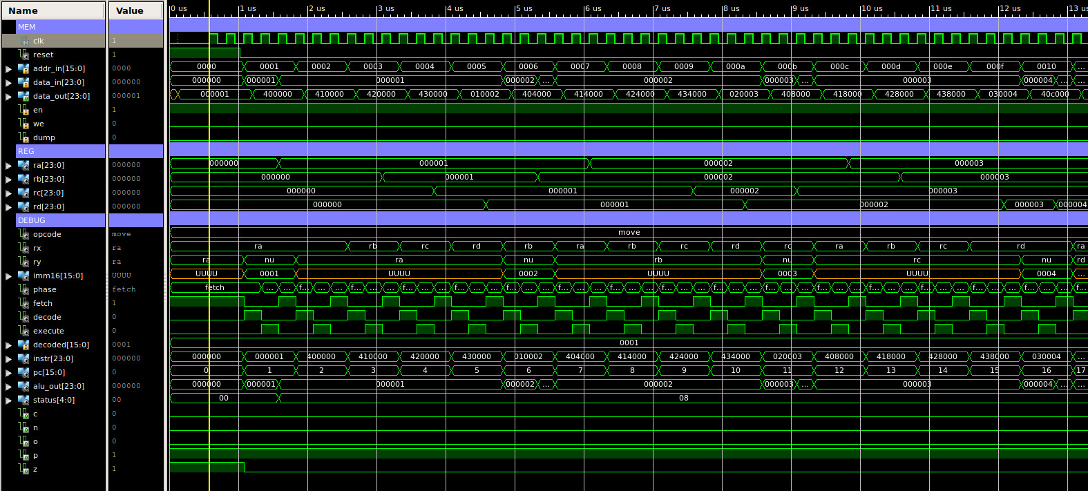
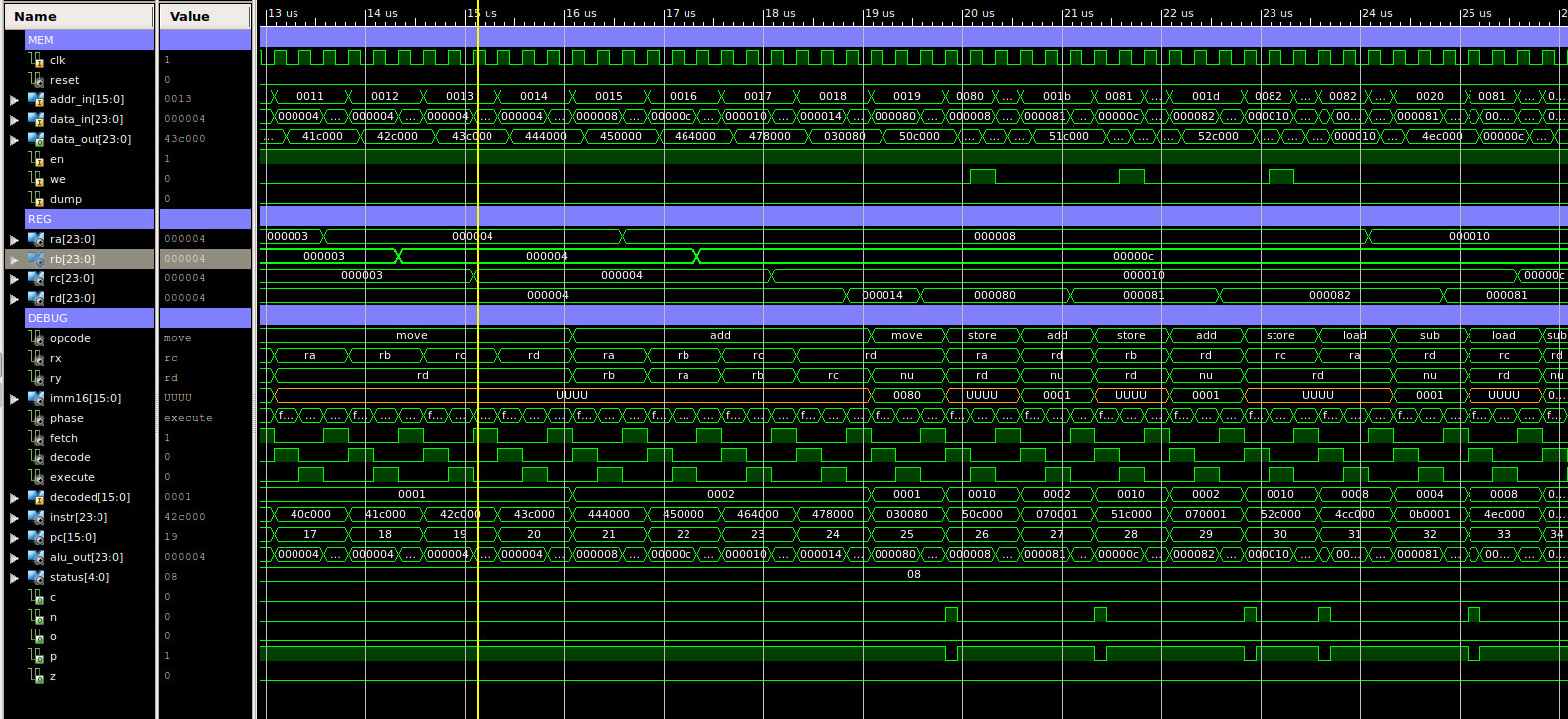

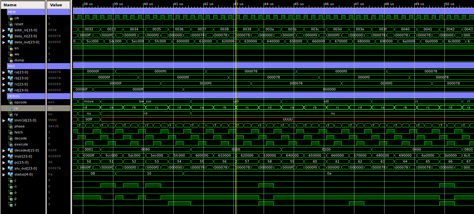
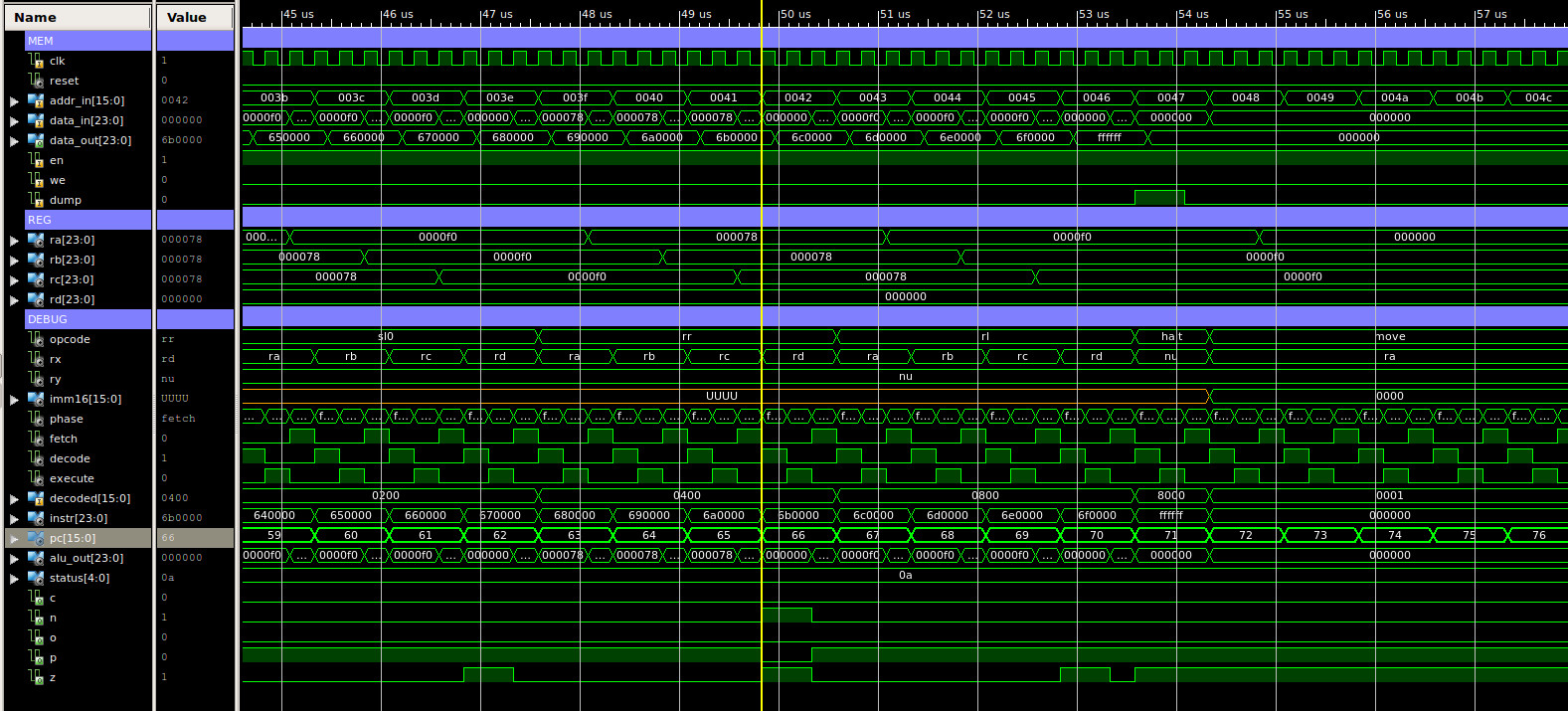
Figure 61 : type-1 instructions simulation
The final test program focuses on control flow instructions e.g. JUMP, testing type-2 instructions, as shown below. A simulation of the processor executing this code is shown in figure 62, this is split into four sections, each approximately 13us long, total simulation time 51us. To test these JUMP instructions a series of "FOR LOOPs" have been constructed e.g. a register is repeatedly decremented, if the register is not zero this processing loop is repeated, if it is zero the loop is exited, if an incorrect jump is performed the program is trapped in an infinite loop to signal an error has occurred i.e. an unconditional jump to the same address, easy to spot in the simulation trace. Again, at first glance we have our normal sea of squiggles, but, between approximately:
The final memory dump file can be accessed here: (Link).
#
# MOVE : RA=3, RB=0xFFFC, RC=0x7FFC, RD=3
#
00 00 0000 00 00000000 00000011
01 00 0000 01 11111111 11111100
02 00 0000 10 01111111 11111100
03 00 0000 11 00000000 00000011
#
# loopZ:
#   RA=RA-1
#   JUMP Z, 8  (loopC)
#   JUMP NZ, 4 (loopZ)
#   JUMP U 7   (trap)
#
04 00 0010 00 00000000 00000001
05 10 0001 00 00000000 00001000
06 10 0010 00 00000000 00000100
07 10 0000 00 00000000 00000111
#
#  loopC:
#    RB=RB+1
#    JUMP C, 12 (loopO)
#    JUMP NC, 8 (loopC)
#    JUMP U, 11 (trap)
#
08 00 0001 01 00000000 00000001
09 10 0011 00 00000000 00001100
10 10 0100 00 00000000 00001000
11 10 0000 00 00000000 00001011
#
# loopO:
#   RC=RC+1
#   JUMP O, 16  (loopN)
#   JUMP NO, 12 (loopO)
#   JUMP U, 15  (trap)
#
12 00 0001 10 00000000 00000001
13 10 1001 00 00000000 00010000
14 10 1010 00 00000000 00001100
15 10 0000 00 00000000 00001111
#
# loopN:
#   RD=RD-1
#   JUMP N, 20  (testP)
#   JUMP NN, 16 (loopN)
#   JUMP U, 19  (trap)
#
16 00 0010 11 00000000 00000001
17 10 0101 00 00000000 00010100
18 10 0110 00 00000000 00010000
19 10 0000 00 00000000 00010011
#
# testP:
#   RA=0xFFFC
# loopP:
#   RA=RA+1
#   JUMP P, 25  (testREG)
#   JUMP NP, 21 (loopP)
#   JUMP U, 24  (trap)
#
20 00 0000 00 11111111 11111100
21 00 0001 00 00000000 00000001
22 10 0111 00 00000000 00011001
23 10 1000 00 00000000 00010101
24 10 0000 00 00000000 00011000
#
# testREG:
#   RB=28
#   JUMP (RB)  (testCALL)
#   JUMP U, 27 (trap)
#
25 00 0000 01 00000000 00011100
26 10 1011 00 01 00000000000000
27 10 0000 00 00000000 00011011
#
# testCALL:
#   CALL 31  (subroutine)
#   DUMP
#   JUMP 30  (trap)
#
28 10 1100 11 00000000 00011111
29 11 1111 11 11111111 11111111
30 10 0000 00 00000000 00011110
#
# subroutine:
#   MOVE RA, 0xFF
#   RET
#
31 00 0000 00 00000000 11111111
32 10 1101 00 11 00000000000000
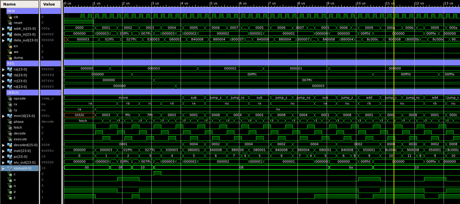
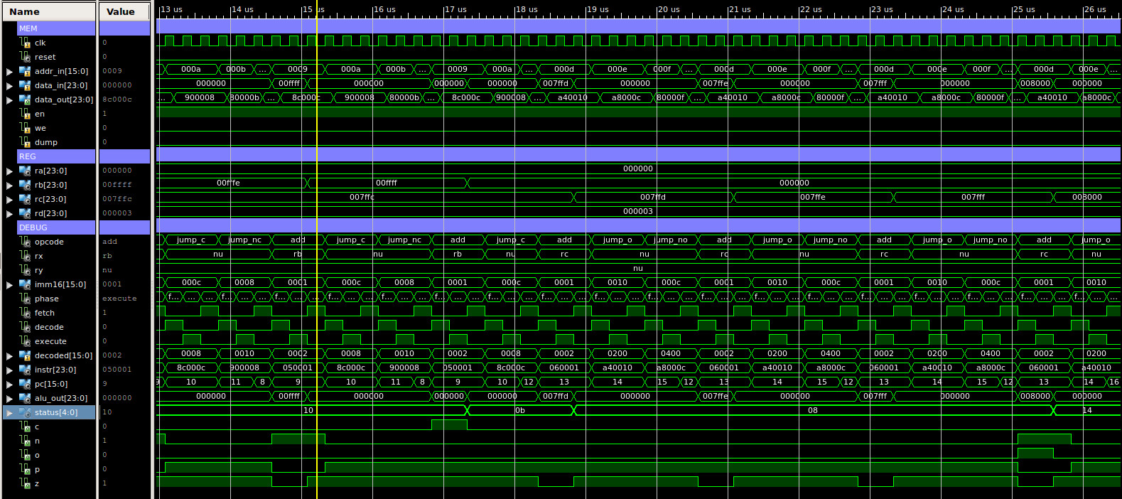
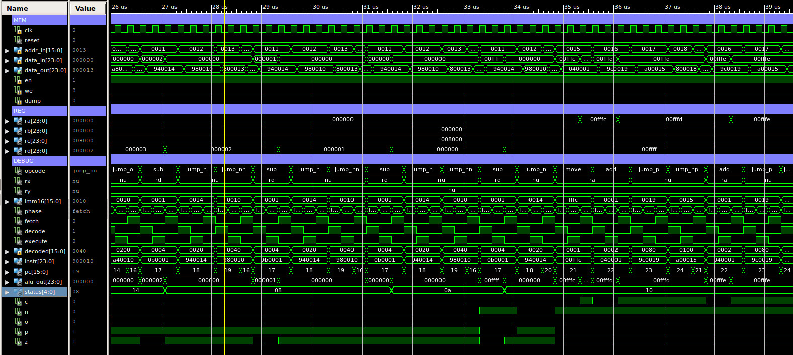
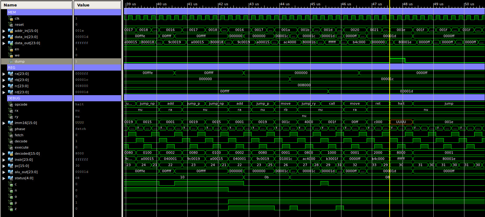
Figure 62 : type-2 instructions simulation
Not a complete test, but all seems good, time to process some images.
To simplify the process of loading images into memory i modified the memory simulation module to automatically load ppm (colour images) and pbm (black and white images) into memory at the start of a simulation. I also modified the DUMP pin so that this memory would also generate ppm and pbm images from the data stored in memory. The entity description of this new memory is shown in figure 63.
Figure 63 : new VHDL memory model
To load a ppm image you set the generic parameter: LOAD_PPM_IMAGE to true, define the start address in memory where the image should be stored and the image file name. Note, image file must be in the same directory as simulation model. The size of the image is taken from the image file. To save a ppm image you set the generic parameter: SAVE_PPM_IMAGE to true, define the start address in memory where the image is stored, the number of rows / columns and the new image file name. I also increased the memory size to the full 64K x 24bits.
To test if this memory model worked i wrote a simple program to read each RGB pixel in the source image, then zero the RG pixels, writing the B pixel value to a new output file i.e. the pixel value is bitwise ANDed with the constant 0xFF. The code for this program is shown below:
#
# Test PPM: B & G
# ---------------
# image size 97 x 60 = 5820
# source start address = 1024 = 0x400
# destination start address = 7000 = 0x1B50
#
# start:
# 00   move RA, 0x0400   -- set read pointer
# 01   move RB, 0x1B50   -- set write pointer
#
# loop:
# 02   load RC, (RA)     -- read input image pixel
# 03   and RC, 0xFF      -- mask off lower byte
# 04   store RC, (RB)    -- write to output image
# 05   add RA, 1         -- increment read pointer
# 06   add RB, 1         -- increment write pointer
# 07   move RC, RA       -- buffer
# 08   sub RC, 0x1ABD    -- is pointer equal to end of input image?
# 09   jump NZ, loop     -- no, repeat
# 10   dump              -- yes, dump memory to file
#
# trap:
# 11   jump trap         -- nothing else to do, so trap program in an infinite loop
#
00 00 0000 00 00000100 00000000
01 00 0000 01 00011011 01010000

02 01 0011 10 00 00000000000000
03 00 0101 10 00000000 11111111
04 01 0100 10 01 00000000000000

05 00 0001 00 00000000 00000001
06 00 0001 01 00000000 00000001

07 01 0000 10 00 00000000000000
08 00 0010 10 00011010 10111101
09 10 0010 00 00000000 00000010
10 11 1111 11 11111111 11111111

11 10 0000 00 00000000 00001011
Running at 10MHz system clock, the simpleCPU processor would take approximately 6us to process each pixel. If the source image has 97 x 60 = 5820 pixels, we will need to run this simulation for 35ms in order to process an image. This doesn't sound a lot, but in the land of simulations this would take a few minutes, therefore, to speed things up i reduced the input image size to 25 x 15, which only takes a few seconds to simulate. Next, modified the bitwise AND mask to 0xFF00, to mask out the G pixel values, then re-ran the simulation. To mask out the R pixel values is a bit more tricky, but still possible. When you perform the bitwise AND with an immediate value the high nibble is set to zero, so the R pixel is always masked. You can perform a bitwise AND on this pixel if you use register addressing as previously discussed in the ALU section above, however, you can not directly set the high byte of a register, as the MOVE instructions writes to the low 16 bits of a register. Note, this type of limitation is quite common in RISC machines i.e. a mismatch between register size and immediate values e.g. you could have a CPU with 64 bit registers, but only a 16 bit immediate. To get over this problem we would normally add a new instruction that loads the 16 bit immediate value into the high 16 bits rather than the low 16 bits, or we could use a barrel shifter in-line with the register file to align any data value using the standard MOVE instructions. However, for the moment going to go for a software solution, to avoid these hardware joys :). An alternative solution is to load a register with the value you want to place in the high byte, then shift left eight time to align this data into the high byte. Code to extract the R pixel value is shown below:
#
# Test PPM
# --------
# image size 25 x 15 = 375
# source start address = 1024 = 0x400
# destination start address = 2048 = 0x0800
#
# start:
# 00   move RA, 0x0400   -- set read pointer
# 01   move RB, 0x0800   -- set write pointer
# 02   move RC, 0xFF00   -- set mask
# 03   move RD, 8        -- set loop count
#
# loop1:
# 04   sl0 RC            -- shift mask 8 times to the left
# 05   sub RD, 1         -- is MSB byte updated?
# 06   jump NZ, loop1    -- no, repeat
#
# loop2:
# 07   load RD, (RA)     -- read pixel from input image
# 08   and RD, RC        -- mask low byte
# 09   store RD, (RB)    -- write to output image
# 10   add RA, 1         -- increment read pointer
# 11   add RB, 1         -- increment write pointer
# 12   move RD, RA       -- buffer
# 13   sub RD, 0x0577    -- is pointer equal to end of input image?
# 14   jump NZ, loop2    -- no, repeat
# 15   dump              -- yes, dump memory to file
#
# trap:
# 16   jump trap         -- nothing else to do, so trap program in an infinite loop
#
00 00 0000 00 00000100 00000000
01 00 0000 01 00001000 00000000
02 00 0000 10 11111111 00000000
03 00 0000 11 00000000 00001000

04 01 1001 10 00000000 00000000
05 00 0010 11 00000000 00000001
06 10 0010 00 00000000 00000100

07 01 0011 11 00 00000000000000
08 01 0101 11 10 00000000000000
09 01 0100 11 01 00000000000000

10 00 0001 00 00000000 00000001
11 00 0001 01 00000000 00000001

12 01 0000 11 00 00000000000000
13 00 0010 11 00000101 01110111
14 10 0010 00 00000000 00000111
15 11 1111 11 11111111 11111111

16 10 0000 00 00000000 00010000
The new, smaller source image and the three output images are shown in figures 64 to 67. Note, these images have been scaled up to 600 x 300 for the web page, 25 x 15 is very small :). Looking at these images you can clearly see that Bob the bug is a greeny-blue, as in the red pixel image he is almost black i.e. has very low levels of red. The intensity or brightness of each pixel is given by the weighted sum of the R + G + B values.

Figure 64 : new source image - 25 x 15

Figure 65 : R pixels only output image

Figure 66 : G pixels only output image

Figure 67 : B pixels only output image
To test if pbm images could be stored in the new memory model i implemented a simple threshold algorithm to convert a colour image into a black and white image. The program performs the addition of the R, G and B pixel values to calculate the pixels brightness, if its value is above a defined threshold the corresponding output pixel is set white, otherwise it is set black. In the land of image processing the "brightness" (Y) can mean different things e.g. mean brightness, perceived brightness, luminance etc. Two commonly used equations used to calculate "brightness" (Y):
Y = (R + G + B) / 3
Y = 0.33 R + 0.5 G + 0.16 B
Given the current instruction set we don't have general purpose multiplication or division instructions. However, as we are only looking to see if the pixels brightness is greater than a threshold the first of the above equations could be implemented by simply removing the divide by 3 and multiplying the threshold by 3. As the threshold is a constant this can be done before run-time. The second equation may look a bit more of an issue as we are dealing with fractional values, however, again with a little bit of sideways thinking we can get an approximate solution. Multiplication can be implemented using repeated addition e.g. R+R+R = 3 x R. For small values this isn't a big overhead, however, for larger values e.g. 1000 x R, it starts to become impractical. Division can be implemented using shift right instructions, each shift to the right divides by 2. Therefore, the second equation can be rewritten as:
Y = (0.375 R)    + (0.5 G)   + (0.125 B)
Y = (3/8 x R)    + (1/2 x G) + (1/8 x B)
Y = (R+R+R)>>3   + (G)>>1    + (B)>>3
Y = (R+R+R+B)>>3 + (G)>>1
Note "X >> N" reads as variable X is shifted right N bit positions. As we are limited by a fixed divide by 2, we can not get exactly the same weighting e.g. 0.375 rather than 0.33, however, for some algorithms this is close enough. To keep things simple went for the first solution, multiplying the threshold by 3. To prototype this algorithm i implemented a simple solution in python: (Link)
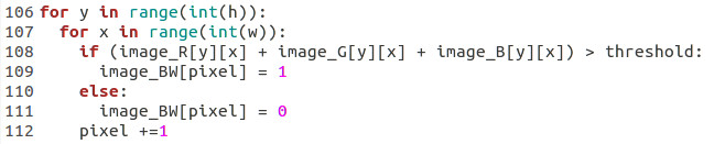
Figure 68 : Threshold algorithm main loop
With a threshold of 80x3=240, this code produced the images shown in figure 69. Note, in the new image bright pixels i.e. greater than the threshold are set black, and dark pixels i.e. less than threshold are set white e.g. the white base is now black.

Figure 69 : Threshold algorithm - input image (left), output image (right)
This algorithm can be implemented on the simpleCPU using the code listed below. This is the first non-trivial program, a bit to think about here i.e. what variables do we need to store, how should the registers be used etc. This program also highlights a mismatch between algorithm, instruction-set and hardware. To add the R, G and B terms together we need to mask and shift the pixel values, to extract each of the three 8bit values. This negates the advantage of using a 24 bit data width. Ideally we would add a new instruction and hardware that could add together these three values in one operation, as shown in figure 70.
#
# Test PBM
# --------
# image size 25 x 15 = 375
# source start address = 1024 = 0x400
# destination start address = 2048 = 0x0800
#
# Variables
# ---------
# read_pntr  = 0x40
# write_pntr = 0x41
# accumlator = 0x42
# pixel_cnt  = 0x43
#
# start:
# 00   move RA, 0x0400   -- initialise external variables
# 01   store RA, 0x40    -- read pointer
# 02   move RA, 0x0800
# 03   store RA, 0x41    -- write pointer
# 04   move RA, 1
# 05   store RA, 0x43    -- pixel set-mask/counter (bits used in current 24bit memory location)
#
# loop1:
# 06   move RA, 0
# 07   store RA, 0x42    -- accumulator for R + G + B
#
# 08   load RA, 0x40     -- read RGB pixel
# 09   load RD, (RA)
# 10   move RB, 3        -- set RGB accumulator loop count
#
# loop2:
# 11   move RC, RD       -- buffer pixel
# 12   and  RC, 0xFF     -- mask low byte
# 13   load RA, 0x42     -- read accumulator
# 14   add RC, RA        -- add byte to accumulator
#
# 15   sub RB, 1         -- have we done this 3 times?
# 16   jump Z, update (23)   -- yes, update output image
# 17   store RC, 0x42    -- no, update loop count
# 18   move RA, 8        -- set shift loop count
#
# loop3:
# 19   sr0 RD            -- shift right pixel data 8 times
# 20   sub RA, 1         -- decrement loop count
# 21   jump NZ, loop3 (19)    -- zero?
# 22   jump loop2 (11)       -- yes, repeat accumulation
#
# update:
# 23   load RB, 0x43     -- read set-mask/count
# 24   load RA, 0x41     -- read current output image memory location
# 25   load RD, (RA)     --
# 26   sub RC, 0xF0      -- is accumulated R + G + B value > 240?
# 27   jump N, smaller (30)  -- no
#
# larger:
# 28   or RD, RB         -- yes, set bit.
# 29   store RD, (RA)    -- update current output image memory location

# smaller:
# 30   sl0 RB            -- update mask/count
# 31   store RB, 0x43    --
# 32   jump NZ, continue (38)

# 33   move RB, 1        -- reset count
# 34   store RB, 0x43    --
# 35   load RB, 0x41     -- yes, load write pointer
# 36   add RB, 1         -- increment write pointer
# 37   store RB, 0x41    -- save new write pointer
#
# continue:
# 38   load RA, 0x40     -- load read pointer
# 39   add RA, 1         -- increment read pointer
# 40   store RA, 0x40    -- save new read pointer
# 41   move RB, RA       -- buffer pointer
# 42   sub RB, 0x0577    -- have all input image pixels been processed?
# 43   jump NZ, loop1 (6)   -- no, repeat
# 44   dump              -- yes, dump memory to file
#
# trap:
# 45   jump trap (45)        -- nothing else to do, so trap program in an infinite loop
#
00 00 0000 00 00000100 00000000
01 00 0100 00 00000000 01000000
02 00 0000 00 00001000 00000000
03 00 0100 00 00000000 01000001
04 00 0000 00 00000000 00000001
05 00 0100 00 00000000 01000011
#
06 00 0000 00 00000000 00000000
07 00 0100 00 00000000 01000010
#
08 00 0011 00 00000000 01000000
09 01 0011 11 00 00000000000000
10 00 0000 01 00000000 00000011
#
11 01 0000 10 11 00000000000000
12 00 0101 10 00000000 11111111
13 00 0011 00 00000000 01000010
14 01 0001 10 00 00000000000000
#
15 00 0010 01 00000000 00000001
16 10 0001 00 00000000 00010111
17 00 0100 10 00000000 01000010
18 00 0000 00 00000000 00001000
#
19 01 1000 11 00000000 00000000
20 00 0010 00 00000000 00000001
21 10 0010 00 00000000 00010011
22 10 0000 00 00000000 00001011
#
23 00 0011 01 00000000 01000011
24 00 0011 00 00000000 01000001
25 01 0011 11 00 00000000000000
26 00 0010 10 00000000 11110000
27 10 0101 00 00000000 00011110
#
28 01 0110 11 01 00000000000000
29 01 0100 11 00 00000000000000
#
30 01 1001 01 00000000 00000000
31 00 0100 01 00000000 01000011
32 10 0010 00 00000000 00100110
#
33 00 0000 01 00000000 00000001
34 00 0100 01 00000000 01000011
35 00 0011 01 00000000 01000001
36 00 0001 01 00000000 00000001
37 00 0100 01 00000000 01000001
#
38 00 0011 00 00000000 01000000
39 00 0001 00 00000000 00000001
40 00 0100 00 00000000 01000000
41 01 0000 01 00 00000000000000
42 00 0010 00 00000101 01110111
43 10 0010 00 00000000 00000110
44 11 1111 11 11111111 11111111
#
45 10 0000 00 00000000 00101101
To process each pixel takes 68us, therefore, reduce image size down to 25 x 15 to reduce processing time, but this still requires 26 ms, which takes a few minutes to simulate :(. The program structure is as follows, lines:

Figure 70 : Possible hardware improvement
The final processed image are shown in figures 71 and 72. Note, when you scale the image down to 25 x 15 you have to use your imagination :).

Figure 71 : 25 x 15 PPM input image

Figure 72 : 25 x 15 PBM output image

Figure 73 : GPIO
Doesn't matter what the processor, you do need a "Hello World" program :). A simple 8bit GPIO port can be mapped into the processors address space using the top two address bits and a 2-to-4 one-hot decoder. This divides the address space into four 16K blocks, as shown below:
  SEL   :                         BITS                              :    HEX   :   FUNC
A15 A14    A13 A12 A11 A10 A09 A08 A07 A06 A05 A04 A03 A02 A01 A00
0   0   :  0   0   0   0   0   0   0   0   0   0   0   0   0   0    :  0x0000  :   RAM
0   0   :  1   1   1   1   1   1   1   1   1   1   1   1   1   1    :  0x3FFF  :

0   1   :  0   0   0   0   0   0   0   0   0   0   0   0   0   0    :  0x4000  :   GPIO
0   1   :  1   1   1   1   1   1   1   1   1   1   1   1   1   1    :  0x7FFF  :

1   0   :  0   0   0   0   0   0   0   0   0   0   0   0   0   0    :  0x8000  :   NU
1   0   :  1   1   1   1   1   1   1   1   1   1   1   1   1   1    :  0xBFFF  :

1   1   :  0   0   0   0   0   0   0   0   0   0   0   0   0   0    :  0xCFFF  :   NU
1   1   :  1   1   1   1   1   1   1   1   1   1   1   1   1   1    :  0xFFFF  :
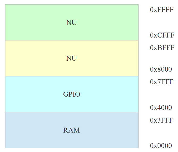
Figure 74 : Full memory map
Note, the RAM and GPIO do not use their full assigned 16K block i.e. the RAM is limited to a 4K x 24bit device and the GPIO only has one active location. A "zoomed" in view of the two active memory blocks is shown in figure 74. To address the 16K block requires 14bits, however, the RAM only uses 12bits to address its 4K locations, leaving two unused address lines: A13 and A12. Therefore, when the processor reads through this 16K block it will read through the RAM's 4K address space four times i.e. the blocks labelled RAM are the same 4K RAM, repeated through the 16K address space e.g.
RAM ADDR 0x0000 = 0x1000 = 0x2000 = 0x3000
RAM ADDR 0x0001 = 0x1001 = 0x2001 = 0x3001
RAM ADDR 0x0FFF = 0x1FFF = 0x2FFF = 0x3FFF
As the GPIO does not use the address bus if the processor writes to any location between 0x4000 to 0x7FFF it will update the output port, or if its reads any of these memory locations it will access the input port.
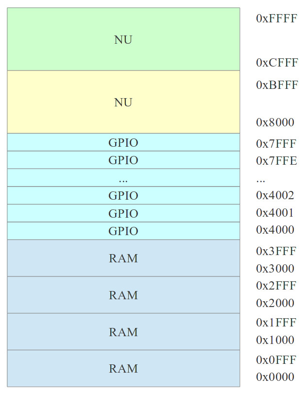
Figure 74 : Used memory map
The output port is 8 bits wide, therefore, when writing to this device only the lower 8bits of the CPU's 24bit data bus are active. The ASCII characters are transmitted using a RS232 serial port, as described in the first simpleCPU (Link). To transmit the message we only need one output bit (TX) and a 0V reference line. Note, the two communicating devices always need to agree on what the signal's voltage levels are referenced to i.e. a common 0V or GND line. The speed at which the serial data is transmitted is controlled by software, 9600 bits-per-second (bps). This means that each bit is active (time slice) on the TX line for:
1/9600 = 0.000104167 = 104us
Knowing the CPU's clock speed we can implement this delay by simply burning through CPU cycles using a FOR loop. For the moment we will ignore software overheads associated with setting and clearing the output line, therefore:
#
# SW DELAY LOOP
#
delay:
   move RC, 0xAD
loop:
   sub RC, 1
   jump NZ, loop
   ret

Clock = 10MHz
Period = 1/10x10^6 = 0.0000001 = 0.1us

Clock cycles per bit slice = 104us / 0.1us = 1041.67
Number of clock cycles per instruction = 3

Number of instructions in delay loop = 1042 / 3 = 347 = 0x15B
Number of instructions = 1 + (2 x C) + 1 = 347 = (347-2)/2 = 171 = 0xAD
The complete program is shown below, ASCII characters are stored at the end of the program, as 8 bit values, to simplify data access only one character is stored in each memory location.
#
# HELLO WORLD
# -----------
#
#   move RA, 1      -- tx start bit
#   store RA, 0x
#   call delay
#
#   load RA, 0x11   -- load read pointer
#
# char:
#   load RB, (RA)   -- read char
#   and RB, 0xFF    -- if EOL (zero) exit
#   jump Z, stop
#
#   load RA, 8      -- bit count
#
# tx:
#   move RD, RB
#   and RD, 1
#   store RD, 0x    -- tx bit
#   call delay
#
#   sr0 RB
#   sub RA, 1
#   jump NZ, tx
#
#   load RA, 0x11   -- load read pointer
#   add RA, 1
#   store RA, 0x11
#   jump start
#
# stop:
#   move RA, 0      -- tx stop bit
#   store RA, 0x
#   call delay
#
#   jump start
#
# delay:
#   move RC, 0xAD
# loop:
#   sub RC, 1
#   jump NZ, loop
#   ret
#
# data:
#   H - 0100 1000
#   e - 0110 0101
#   l - 0110 1100
#   l - 0110 1100
#   o - 0110 1111
#  SP - 0010 0000
#   W - 0101 0111
#   o - 0110 1111
#   r - 0111 0010
#   l - 0110 1100
#   d - 0110 0100

00 00 0000 00 00000100 00000000
00 00 0000 00 00000000 00000000

00 00000000 0000 0000 0100 1000
00 00000000 0000 0000 0110 0101
00 00000000 0000 0000 0110 1100
00 00000000 0000 0000 0110 1100
00 00000000 0000 0000 0110 1111
00 00000000 0000 0000 0010 0000
00 00000000 0000 0000 0101 0111
00 00000000 0000 0000 0110 1111
00 00000000 0000 0000 0111 0010
00 00000000 0000 0000 0110 1100
00 00000000 0000 0000 0110 0100
The least significant bit of the output bit is used as the TX bit, passed through a level shifter, as shown in figure 75, to produce a bi-polar signal.
WORK IN PROGRESS

This work is licensed under a Creative Commons Attribution-NonCommercial-NoDerivatives 4.0 International License.
Contact email: mike@simplecpudesign.com