I had to stop work on the TTL version of the SimpleCPU, as where I work there have been changes in Health and Safety rules. To cut a very long story short i'm no longer allowed to solder, so building things at work is a bit of an issue :(. Therefore, my thoughts moved to another implementations of the SimpleCPU that ive been avoiding, a pipelined version. Again, the emphasis here is not to design the world's best processor, rather to create a design that is focused on teaching i.e. a pipelined cpu that demonstrates the advantages of pipelining, but also exposes its issues in terms of its hardware implementation. Therefore, this CPU will not be the fastest, but it will demonstrate key design considerations and how these affects the CPUs architecture, its instruction-set and the software run upon it. As always this will be a working design, implemented as a schematic that can be downloaded onto an FPGA, not just a simulation :).
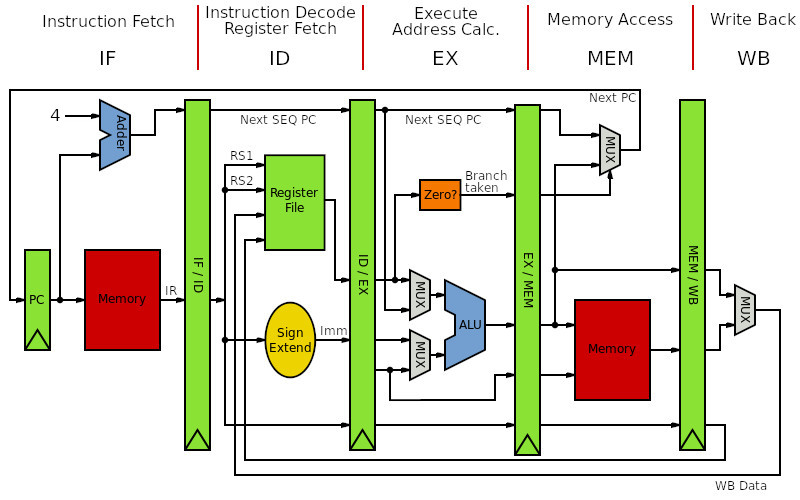
Figure 1 : a Basic MIPS architecture
The starting point of this design is going to be based around a basic MIPS (Link) / DLX (Link), as shown in figure 1. This is a VERY common design used in a lot of existing teaching material. In fact this architecture was the first pipelined processor i studied all those years ago from the classic reference book "Computer Architecture: A Quantitative Approach 2nd Edition", by Hennessy and Patterson. However, although this an excellent book it does abstract away from the low level hardware, hiding implementation details in a block diagrams etc. The example in figure 1 is a good point in case, consider the PC data path, if the next PC was truly passed through the pipeline registers as shown, this CPU isnt actually pipelined i.e. it does not fetch a new instruction on every clock cycle :(. These block diagrams are excellent at getting key points about pipelining across to students, at times you do need to abstract away from all that hardware, but block diagrams are also misleading, or just lack the details needed to truly hammer home these ideas. Therefore, i think there is a hole in the literature to be filled, and what better way to do this than a pipelined version of the SimpleCPU based around this well established architecture. No ISA copyright violations here :).
The MIPS architecture is from the RISC (Link) class of processor. The design emphasis for this family of processors is to maximise instruction throughput, such that the processor can complete an instruction on every clock cycle (once the pipeline is full). Therefore, complex, multi-cycle instructions used in CISC (Link) machines have to be removed from the MIPS instruction-set. Hence this architecture's name: Microprocessor without Interlocked Pipelined Stages i.e. on each clock cycle the processor moves an instruction onto the next processing (pipeline) stage. This allows processing stages to be overlapped i.e. the fetch, decode and execute phases can operate in parallel, as shown in figure 2.
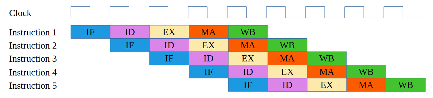
Figure 2 : pipelined instructions
In this version of the MIPS architecture the instruction processing is broken down into five separate stages:
By allowing each processing stage to be overlapped a new instruction is fetched from memory on each clock cycle. Therefore, after five clock cycles the processor will be processing five different instructions i.e. all stages are busy, the processing pipeline is full. Once full one instruction will then complete on each following clock cycle, giving a speed up of 5, when compared to a machine that waits until an instruction completes before fetching the next. There are exceptions to this basic rule, but the key to maximising performance on this architecture is to keep the pipeline full, as shown in figure 3. A second advantage of removing complex functions (hardware) is that the size of the logic in each stage is reduced, reducing its critical path delay i.e. how long it takes a block of combinatorial logic to settle down to a final value. Therefore, smaller, faster logic allows the processor's clock speed to be increased, further improving instruction throughput.
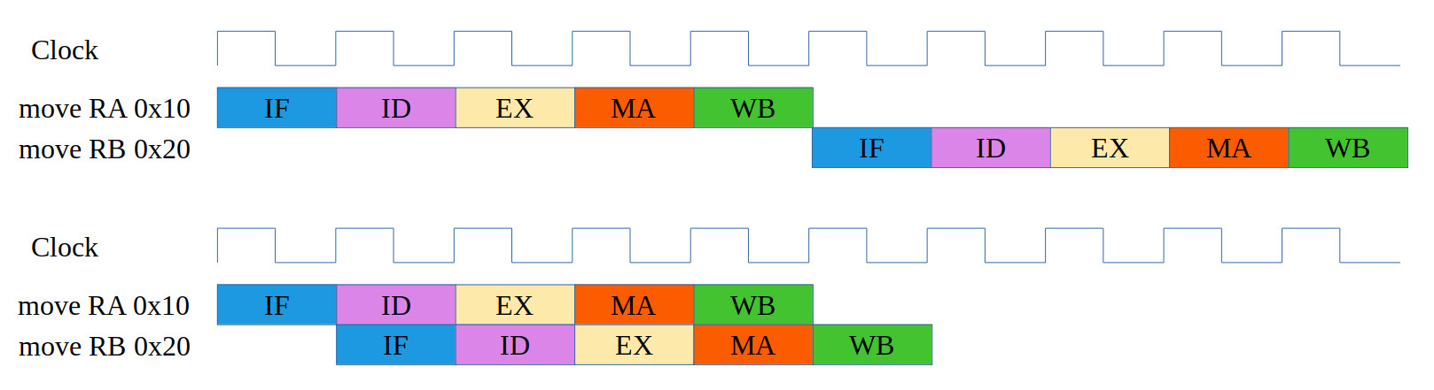
Figure 3 : non-pipelined (top) and pipelined (bottom)instructions
This CPU design emphasis triggered a reconsideration of how processors were designed, what functions should be implemented in hardware and what should be done in software i.e. as a sequence of simple instructions, rather than a single complex instruction. However, the requirement to allow an instruction to complete on each clock cycle has a number of undesirable consequences that limit the types of addressing modes and instructions that can be used on these CPUs. In the SimpleCPU_v1d the absolute addressing mode could be used with the ADD and SUB instructions:
ADD RA 0x100      RA <- RA + M[0x100]
SUB RB 0x55       RB <- RB - M[0x55]
However, the downside of these instructions is that they require two memory accesses i.e. when the instruction is first fetched and then its accesses its operand data. Multiple memory accesses would prevent the next instruction being accessed when pipelining i.e a basic memory architecture only has a single address and data bus, restricting it to a single memory transaction per clock cycle. Therefore, to minimise the occurrence of this issue the only instructions allowed to access operand data from memory are the LOAD and STORE instructions. All other instruction have to access their operands from registers. This gives the RISC architecture its second commonly used name i.e. a LOAD / STORE architecture. This shift in where operands are stored necessitates an increase in the register-file size i.e. we need space to store our temporary variables somewhere, so you typically you see 8, 16 or more general purpose registers in this type of CPU. A downside of this change is the increase in instruction length (bits) owing to the associated increases in register bit-field sizes (RegSel), as shown in figure 4.
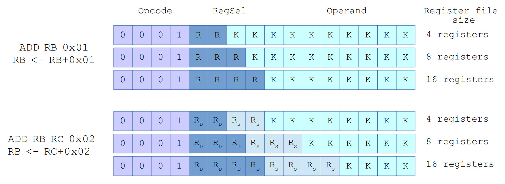
Figure 4 : instruction formats
As the register-file size is increased we need more bits for the register select bit fields (RegSel). This leaves less bits available for the opcode and operand bit fields. If we stick with the same fixed length instruction (16bits) these new instructions will not be capable of representing the desired number ranges etc. Therefore, the instruction length would need to be increased from 16bits to 24bits or 32bits. Increasing memory size / cost etc. In general the increased use of registers to store working variables is a good design optimisation, as it does minimises the number of memory accesses and allows the pipeline to operate correctly. This optimisation also increases processing performance when compared to accessing data from external memory as registers are typically quicker to access.
To state the obvious increasing the register-file size does not remove the memory access problem, we still need the LOAD and STORE instructions to move data between memory and registers. Therefore, we will need to break the golden rule of the MIPS and add an interlock to stop an instruction-fetch when processing the LOAD and STORE instructions i.e. a stall, as shown in figure 5.
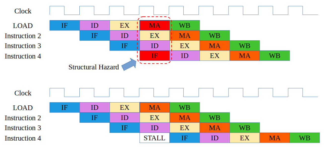
Figure 5 : STORE instruction stall
The issue shown in this example is called a structural hazard, the processor is trying to read two different memory locations on the same clock cycle i.e. the RED blocks, the MA stage for the LOAD instruction and the IF stage for instruction 4. This problem occurs as memory typically only has a single address bus, as shown in figure 6 i.e. a hardware limitation. Typically memory only has a single port i.e. a single address and data bus. However, the memory devices in the FPGA do also support dual port memory i.e. a memory with two separate address and data buses, allowing two memory transactions per clock cycle (slight complexities if read / write to the same memory location). Therefore, we could remove this structural hazard by replacing the single port memory used by the simpleCPU_v1d with a dual port version. Now one memory port would be used for accessing instructions, the other for data accesses. However, i decided not to do this, as dual port memory is not typically used for main memory, also its a good teaching example of a structural hazard in action :).
Note, in the example shown in figure 5 we will assume that instructions 2 - 4 are independent register based instructions i.e. the data accessed by the LOAD instruction is not used by instructions 2 - 4, and their operands are stored in different registers. If not other hazards will occur. Also assume that instructions 2 - 4 are not LOAD / STORE instructions :).
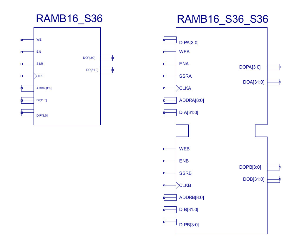
Figure 6 : Memory devices, single port (left), dual port (right)
Therefore, to over come this structural hazard we need to delay the fetch of instruction 4 i.e. delay the issue of instruction 3 in the ID stage until the LOAD instruction has accessed its data. This delay is called a pipeline stall, the act of stopping instructions moving onto the next pipeline stage. This effectively creates "bubbles" into the pipeline i.e. gaps in the instruction flow, where no instruction are being executed, as we allow instructions already in the pipeline to complete. There are two common methods of implementing this stall:
In the MIPS architecture a NOP instruction was created by using the R0 register. This register was not really a register, rather a hardwired constant i.e. if you read R0 you would always get zero and if you wrote a value to R0 it would be lost. Therefore, the instruction ADD R0, R0 i.e. R0 <- R0+R0 does nothing, as the operands fetched are constants and the result of the ADD is discarded. We could do something similar in this processor, however, to avoid adding new instruction or altering the existing register file, i decided to go for the second approach and add a VALID flag to each stage.
Another common problem in a pipelined processor are RAW hazards i.e Read After Write hazards. These occur in a pipelined CPU as an instruction does not complete before we issue the next. Therefore, if the next instruction uses the result of the previous instruction i.e. the result of the instruction ahead of it in the pipeline, when it accesses its operands it will access old operand values, not the new result, as shown in figure 7.
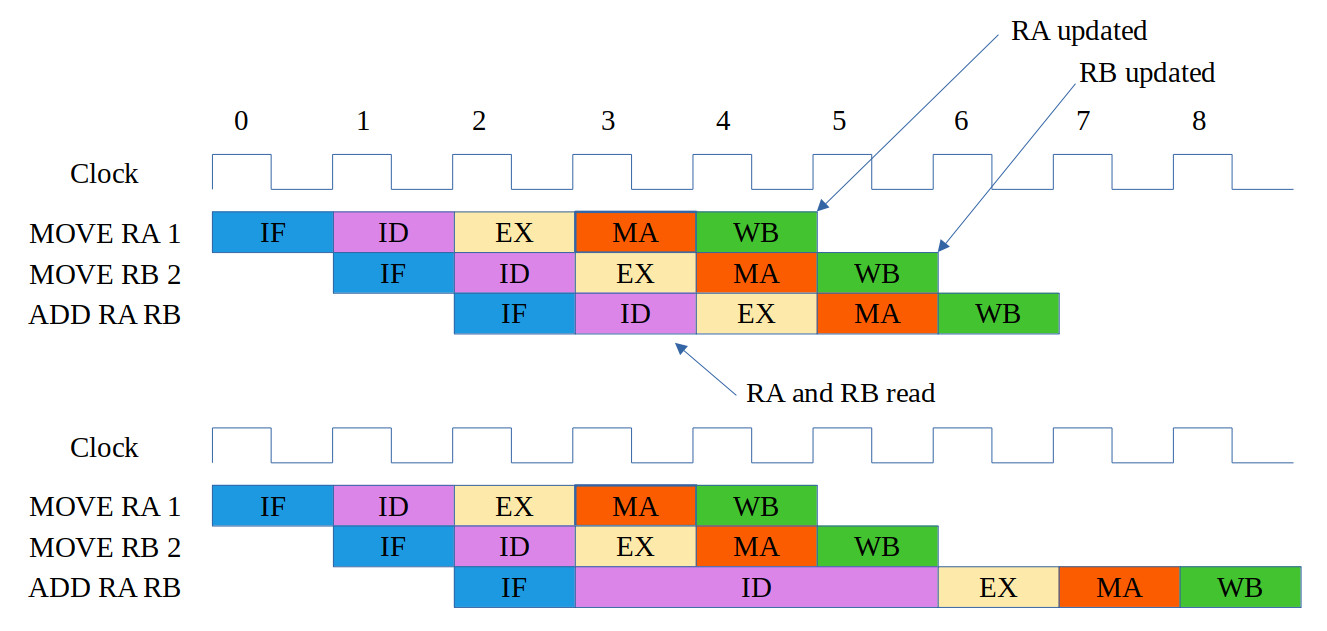
Figure 7 : RAW hazard
In this example the first two MOVE instructions initialise registers RA and RB with the values 1 and 2. These values will be written to the register-file at the end of clock cycle 5. However, the ADD instruction accesses its operands (these values) during its ID stage i.e. clock cycle 3. Therefore, it will access the previous values of RA and RB. Therefore, to prevent this error within the ID stage, the instruction decoder compares the source register fields of the current instruction to the destination register fields of the instructions in the EX, MA and WB stages. If these match, the current instruction is held in the ID phase i.e. stalled, until the matching instructions within the pipeline have written their results to the register file.
There is one final design problem we need to consider for this processor: Control Hazards. Although the SimpleCPU_v1d and the MIPS processor are architecturally similar i.e. they are RISCy rather than CISCy, they have fundamental differences in how they process their instructions. The SimpleCPU_v1d allows an instruction to complete before starting the next, whereas the MIPS overlaps the execution of five instructions within its processing pipeline. This difference is significant when it comes to flow-control instructions i.e. conditional and unconditional jump instructions. A MIPS example is shown in figure 8.
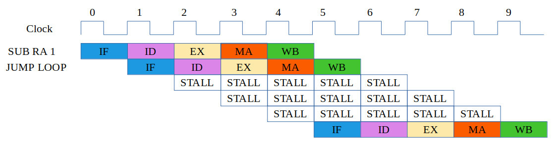
Figure 8: Control hazard
Here, the jump instruction's (JUMP) target address is not selected until the MA phase i.e. cycle 5. Therefore, the pipeline has to stall for three clock cycles until the address of the next instruction is known. On the SimpleCPU_v1d this issue does not occur as each instruction completes before the next instruction is fetched. This issue is further complicated when you consider conditional jum instructions e.g. JUMPZ, JUMPNZ etc. These are typically controlled via flags stored in the processor's' status register:
These flags store the outcome of the last arithmetic or logic instruction, and are globally visible across the processor. The SimpleCPU_v1d's branch instructions shown in figure 9. The top 4bits representing the opcode, the lower 12bit (AAAAAAAAAAAA) the target address. These instructions implementing the IF-THEN-ELSE or FOR/WHILE software structures.
| Instr. | Description | IR15 | IR14 | IR13 | IR12 | IR11 | IR10 | IR09 | IR08 | IR07 | IR06 | IR05 | IR04 | IR03 | IR02 | IR01 | IR00 |
|---|---|---|---|---|---|---|---|---|---|---|---|---|---|---|---|---|---|
| JUMPU | unconditional jump | 1 | 0 | 0 | 0 | A | A | A | A | A | A | A | A | A | A | A | A |
| JUMPZ | jump if zero | 1 | 0 | 0 | 1 | A | A | A | A | A | A | A | A | A | A | A | A |
| JUMPNZ | jump if not zero | 1 | 0 | 1 | 0 | A | A | A | A | A | A | A | A | A | A | A | A |
| JUMPC | jump if carry | 1 | 0 | 1 | 1 | A | A | A | A | A | A | A | A | A | A | A | A |
Figure 9 : SimpleCPU_v1d branch instructions
The unconditional jump instruction JUMPU (or just JUMP) will always jump to the branch target address. For the conditional jump instructions: JUMPZ, JUMPNZ and JUMPC, the branch target address is dependant on the flags stored in the status register. For the SimpleCPU_v1d these indicate the result of the last arithmetic or logic instruction. However, for the MIPS determining this status register's state is a little more complicated, as it could be the result of three different instructions within the pipeline, as shown in figure 10 i.e. the result from the overlapped EX stages.
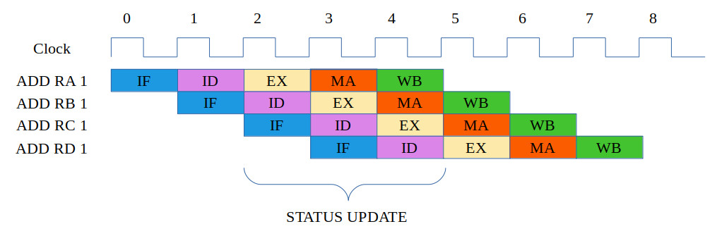
Figure 10: Status register updates
There a different approaches to overcome the issues involved of updating the status register. However, like the previous issue of access operand data from memory, pipelined processors tend to overcome this problem by removing the status register from the processor's architecture and implementing conditional jumps using the value stored in a general purpose register, as shown in the next section (figure 12).
Note, there are other better solutions to overcome structural, RAW and Control hazards. The ones previously discussed i.e. based on stalls, were selected as they are simple to implement in terms of software and hardware.
Owing to the problems (hazards) highlighted in the previous section a pipelined processor''s instruction-set tends to follow a common format. A good example is shown below based on the DLX processor (Link).
| Format | Bits | |||||
|---|---|---|---|---|---|---|
| 31 26 | 25 21 | 20 16 | 15 11 | 10 6 | 5 0 | |
| R-type | 0x0 | Rs1 | Rs2 | Rd | unused | opcode |
| I-type | opcode | Rs1 | Rd | immediate | ||
| J-type | opcode | value | ||||
Figure 11: DLX instruction format
| Instr. | Description | Format | Opcode | Operation (C-style coding) |
|---|---|---|---|---|
| ADD | add | R | 0x20 | Rd = Rs1 + Rs2 |
| ADDI | add immediate | I | 0x08 | Rd = Rs1 + extend(immediate) |
| AND | and | R | 0x24 | Rd = Rs1 & Rs2 |
| ANDI | and immediate | I | 0x0c | Rd = Rs1 & immediate |
| BEQZ | branch if equal to zero | I | 0x04 | PC += (Rs1 == 0 ? extend(immediate) : 0) |
| BNEZ | branch if not equal to zero | I | 0x05 | PC += (Rs1 != 0 ? extend(immediate) : 0) |
| J | jump | J | 0x02 | PC += extend(value) |
| JAL | jump and link | J | 0x03 | R31 = PC + 4 ; PC += extend(value) |
| JALR | jump and link register | I | 0x13 | R31 = PC + 4 ; PC = Rs1 |
| JR | jump register | I | 0x12 | PC = Rs1 |
| LHI | load high bits | I | 0x0f | Rd = immediate << 16 |
| LW | load word | I | 0x23 | Rd = MEM[Rs1 + extend(immediate)] |
| OR | or | R | 0x25 | Rd = Rs1 | Rs2 |
| ORI | or immediate | I | 0x0d | Rd = Rs1 | immediate |
| SEQ | set if equal | R | 0x28 | Rd = (Rs1 == Rs2 ? 1 : 0) |
| SEQI | set if equal to immediate | I | 0x18 | Rd = (Rs1 == extend(immediate) ? 1 : 0) |
| SLE | set if less than or equal | R | 0x2c | Rd = (Rs1 <= Rs2 ? 1 : 0) |
| SLEI | set if less than or equal to immediate | I | 0x1c | Rd = (Rs1 <= extend(immediate) ? 1 : 0) |
| SLL | shift left logical | R | 0x04 | Rd = Rs1 << (Rs2 % 8) |
| SLLI | shift left logical immediate | I | 0x14 | Rd = Rs1 << (immediate % 8) |
| SLT | set if less than | R | 0x2a | Rd = (Rs1 < Rs2 ? 1 : 0) |
| SLTI | set if less than immediate | I | 0x1a | Rd = (Rs1 < extend(immediate) ? 1 : 0) |
| SNE | set if not equal | R | 0x29 | Rd = (Rs1 != Rs2 ? 1 : 0) |
| SNEI | set if not equal to immediate | I | 0x19 | Rd = (Rs1 != extend(immediate) ? 1 : 0) |
| SRA | shift right arithmetic | R | 0x07 | as SRL & see below |
| SRAI | shift right arithmetic immediate | I | 0x17 | as SRLI & see below |
| SRL | shift right logical | R | 0x06 | Rd = Rs1 >> (Rs2 % 8) |
| SRLI | shift right logical immediate | I | 0x16 | Rd = Rs1 >> (immediate % 8) |
| SUB | subtract | R | 0x22 | Rd = Rs1 - Rs2 |
| SUBI | subtract immediate | I | 0x0a | Rd = Rs1 - extend(immediate) |
| SW | store word | I | 0x2b | MEM[Rs1 + extend(immediate)] = Rd |
| XOR | exclusive or | R | 0x26 | Rd = Rs1 ^ Rs2 |
| XORI | exclusive or immediate | I | 0x0e | Rd = Rs1 ^ immediate |
Figure 12: DLX instruction-set
The instruction set of the new pipelined SimpleCPU will be a cut down version of the DLX processor's. However, do want to keep a similar style to the original simpleCPU_v1d e.g. the LOAD and STORE instructions have to use register RA for the source/destination register. However, like the MIPS processor these instructions use a new addressing mode: displacement. As previously discussed only the LOAD and STORE instructions can now access data in memory, so i have expanded the register-file to 8 general purpose data registers: RA,RB,RC,RD,RE,RF,RG and RH. I have also removed the status register, making conditional JUMP instructions conditional on a general purpose register, the same as the MIPS processor. This also requires a new addressing mode: relative, as these conditional jump instruction no longer have enough bits to represent the 12bit target address, now PC offset by +254 to -255. The CALL and RET instructions have also been replaced with the MIPS style JAL and JR i.e. the processor no longer has an internal CALL/RET stack, rather the return address is placed in register RH. The CALL/RET stack is now implemented in external memory using software. For initial testing the ISA is limited to:
 INSTR   IR15 IR14 IR13 IR12 IR11 IR10 IR09 IR08 IR07 IR06 IR05 IR04 IR03 IR02 IR01 IR00    Operation (C-style coding)

 MOVE    0    0    0    0    Rd   Rd   Rd    X    K    K    K    K    K    K    K    K      Rd = sign_extend( immediate )
 ADD     0    0    0    1    Rd   Rd   Rd    X    K    K    K    K    K    K    K    K      Rd = Rd + sign_extend( immediate )
 SUB     0    0    1    0    Rd   Rd   Rd    X    K    K    K    K    K    K    K    K      Rd = Rd - sign_extend( immediate )
 AND     0    0    1    1    Rd   Rd   Rd    X    K    K    K    K    K    K    K    K      Rd = Rd & ( immediate )

 LOAD    0    1    0    0    Rs   Rs   Rs    A    A    A    A    A    A    A    A    A      RA = MEM[Rs + sign_extend( value )]
 STORE   0    1    0    1    Rs   Rs   Rs    A    A    A    A    A    A    A    A    A      MEM[Rs + sign_extend( value )] = RA

 JUMPU   1    0    0    0     A    A    A    A    A    A    A    A    A    A    A    A      PC = value
 JUMPZ   1    0    0    1    Rs   Rs   Rs    A    A    A    A    A    A    A    A    A      PC = PC + (Rs == 0 ? sign_extend( value ) : 0)
 JUMPNZ  1    0    1    0    Rs   Rs   Rs    A    A    A    A    A    A    A    A    A      PC = PC + (Rs != 0 ? sign_extend( value ) : 0)

 JAL     1    1    0    0     A    A    A    A    A    A    A    A    A    A    A    A      RH = PC+1; PC = value
 JR      1    1    1    1    Rs   Rs   Rs    X    X    X    X    X    0    0    0    0      PC = Rs

 MOVE    1    1    1    1    Rd   Rd   Rd   Rs   Rs   Rs    X    X    0    0    0    1      Rd = Rs
 ADD     1    1    1    1    Rd   Rd   Rd   Rs   Rs   Rs    X    X    0    0    1    0      Rd = Rd + Rs
 SUB     1    1    1    1    Rd   Rd   Rd   Rs   Rs   Rs    X    X    0    0    1    1      Rd = Rd - Rs
 AND     1    1    1    1    Rd   Rd   Rd   Rs   Rs   Rs    X    X    0    1    0    0      Rd = Rd & Rs
Figure 13: Pipelined simpleCPU instruction-set
To speed up initial develop i implemented the prototype in VHDL i.e. a lot quicker to write some HDL than to draw a schematic. This processor was based on the simpleCPU_v1d with a few "small" alterations. The automatic RTL schematic (for what its worth) is shown in figure 14.
Figure 14: pipelined simplecpu schematic
To test if this processor is working correctly we need to devise a series of testcases to test how this hardware handles: Structural, RAW and Control hazards.
ASSEMBLY CODE              COMMENTS                        ADDR     MACHINE CODE
-------------              --------                        ----     ------------
LOAD RA 0(RA)    # RA = 0100 0000 0000 0000 = 0x4000       0000   0100000000000000
MOVE RB 1        # RB = 1 = 0x0001                         0001   0000001000000001
MOVE RC 2        # RC = 2 = 0x0010                         0002   0000010000000010
MOVE RD 3        # RD = 3 = 0x0011                         0003   0000011000000011
MOVE RE 4        # RE = 4 = 0x0100                         0004   0000100000000100
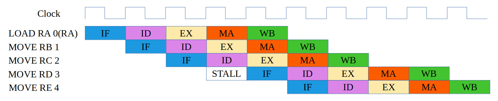
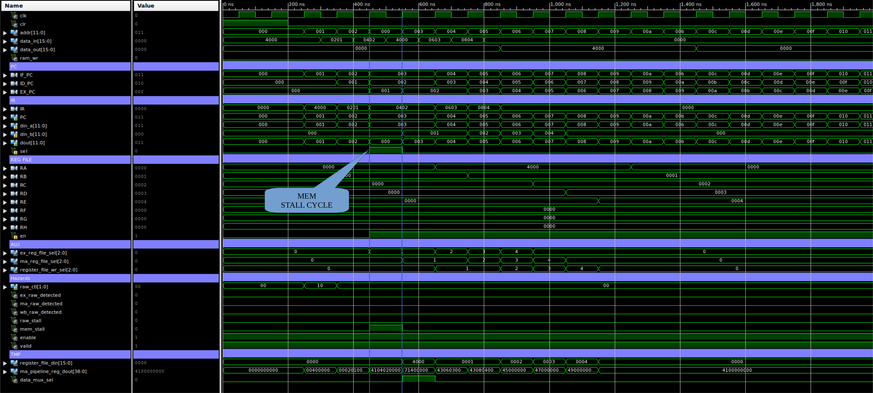
Figure 15: test case 1a, code (top), correct execution (middle), simulation (bottom)
The initial value of RA=0, therefore the LOAD instruction will load itself i.e. the bit pattern that represents LOAD RA 0(RA) into RA. The remaining MOVE instruction load the values 1 - 4 into registers RB - RE. If all is working correctly the above values will be loaded into registers RA - RE. Unfortunately this first test case broke the hardware :). Not in a way i would guess, the hardware did detect the structural hazard correctly, rather that the first instruction caused the processor to lock i.e. the LOAD RA 0(RA) incorrectly detected that RA was being read as the pipeline registers were reset to 0. This incorrectly signalled instructions were in the pipeline that were going to write to register RA. Therefore, the instruction LOAD RA 0(RA) was never released from the decode stage. Solution, needed a hardware flag to signal if the EX, MEM and WB stages were empty. Went for a quick and dirty solution i.e. an extra shift register (stage_enable in waveform diagram), maybe will come back to this one, but it works.
ASSEMBLY CODE        COMMENTS        ADDR     MACHINE CODE
-------------        --------        ----     ------------
LOAD RA 5(RA)    # RA = 0x000A       0000   0100000000000101
LOAD RA 6(RB)    # RA = 0x000B       0001   0100001000000110
LOAD RA 7(RC)    # RA = 0x000C       0002   0100001000000111
LOAD RA 8(RD)    # RA = 0x000D       0003   0100001000001000
LOAD RA 9(RE)    # RA = 0x000E       0004   0100001000001001

DATA 0xA                             0005   0000000000001010
DATA 0xB                             0006   0000000000001011
DATA 0xC                             0007   0000000000001100
DATA 0xD                             0008   0000000000001101
DATA 0xE                             0009   0000000000001110
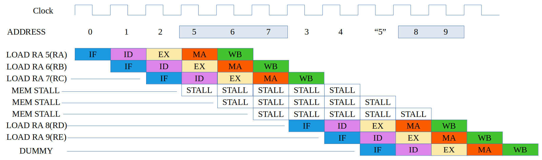
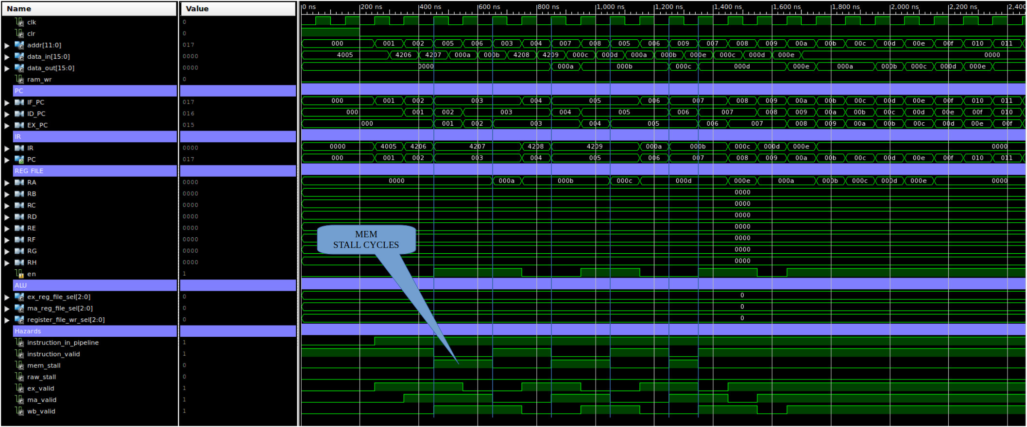
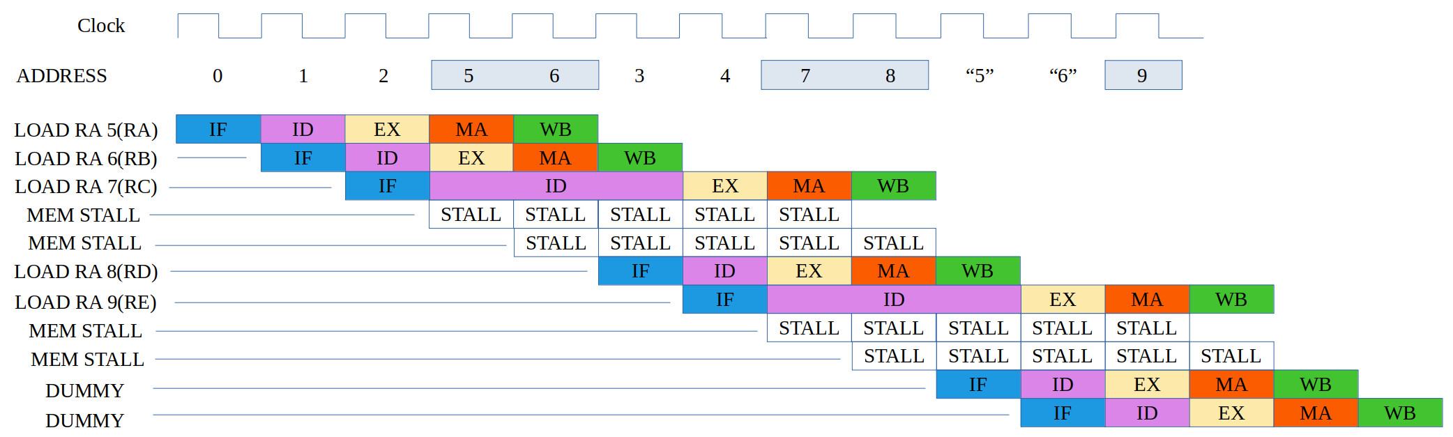
Figure 16: test case 1b, code (top), correct execution (top middle), simulation (bottom middle), actual execution (bottom)
Owing to the limitation of the LOAD instruction the value read from memory has to be stored in register RA, so the above program does not make any practical sense as the values read from memory are being overwritten i.e. only the last LOAD result can be accessed by other instruction. However, i thought this would be an interesting test case to test if the displacement addressing mode was functioning correctly i.e. changing the offset. Note, initial values in RA - RE are assumed to be 0 i.e. reset. Like the first test case this code also failed :(. This issue with this testcase was that the series of LOAD instructions resulted in the structural hazard detection hardware locking the pipeline i.e. the hardware stopped fetching instructions after the third LOAD. This error does not occur for a single LOAD i.e. when there is a mix of memory and register based instructions, as used in figure 15. To solve this issue i made some adjustments to the hazard detection hardware. This "solved" the issue, however, the instruction timing was not as expected, not the same as shown in figure 16 (top). Now the third LOAD instruction's stall behaviour is slightly different, as shown in figure 16 (bottom). The current solution does "work", but the ID phase is held for one cycle more than expected. Looking at the memory transactions there are no wasted cycles, so can be argued this is just as efficient, but i could not find an easy fit to produce the original behaviour. Again, this is something that i will need to have a second look at.
RAW hazards occur when you try to read data (register) before it has been written to a register. These types of hazards occur a lot in pipelined processors as we don't allow an instruction to complete before we issue the next.
ASSEMBLY CODE        COMMENTS        ADDR     MACHINE CODE
-------------        --------        ----     ------------
MOVE RA 0x0F     # RA = 0x000F       0000   0000000000001111
STORE RA 7(RB)   # RB = 0x0000       0001   0101001000000111

DATA 0x9                             0002   0000000000001001
DATA 0xA                             0003   0000000000001010
DATA 0xB                             0004   0000000000001011
DATA 0xC                             0005   0000000000001100
DATA 0xD                             0006   0000000000001101
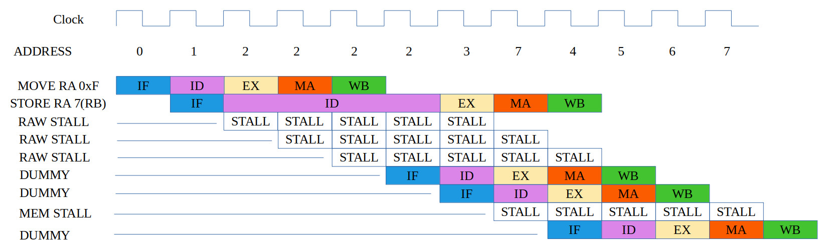
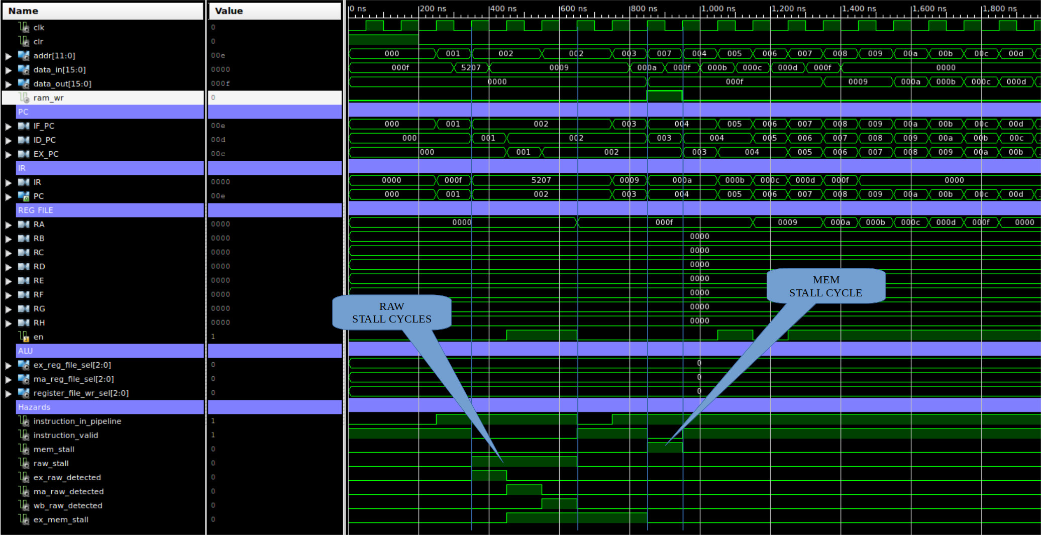
Figure 17: test case 2a, code (top), correct execution (middle), simulation (bottom)
This test code tests for RAW hazards and to again test the displacement addressing mode i.e. the write address should be 7+0=7. Here the value in RA is initialised to 15, therefore, the STORE instruction has to be stalled until the WB phase has completed. The value in RA is then written to memory address 7 (assuming RB=0). This program seemed to work OK :). The instruction timing could be improved by allowing delayed reads i.e. WB write is performed early and ID reads are delayed, allowing the WB and ID phases to overlapped. However, to keep this optimisation back for a later design, i kept in the each ID read cycle. Again, something that i will have a second look at later.
ASSEMBLY CODE        COMMENTS        ADDR     MACHINE CODE
-------------        --------        ----     ------------
MOVE RA 0x0F     # RA = 0x000F       0000   0000000000001111
MOVE RB 0x05     # RB = 0x0005       0001   0000001000000101
STORE RA 7(RB)   #                   0002   0101001000000111

DATA 0x9                             0003   0000000000001001
DATA 0xA                             0004   0000000000001010
DATA 0xB                             0005   0000000000001011
DATA 0xC                             0006   0000000000001100
DATA 0xD                             0007   0000000000001101
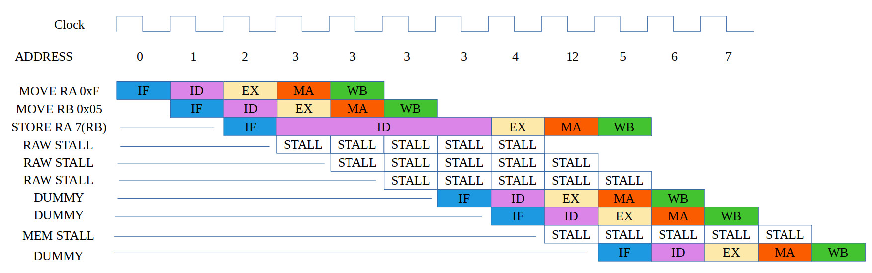
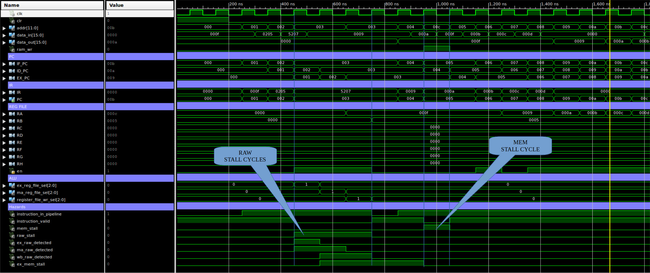
Figure 18: test case 2b, code (top), correct execution (middle), simulation (bottom)
This test code tests for two RAW hazards and to again test the displacement addressing mode i.e. the write address should be 7+5=12. Here the value in RB is initialised to 5, therefore, the STORE instruction has to be stalled until the WB phase for RB has completed. The value in RA is then written to memory address 12. This program seemed to work OK :).
ASSEMBLY CODE        COMMENTS        ADDR     MACHINE CODE
-------------        --------        ----     ------------
MOVE RA 0
MOVE RB 10
MOVE RC 11
MOVE RD 12

LOAD RA 0(RA)
STORE RA 0(RB)
STORE RA 0(RC)
STORE RA 0(RD)
STORE RA 0(RE)
ASSEMBLY CODE        COMMENTS        ADDR     MACHINE CODE
-------------        --------        ----     ------------
LOAD RA 4(RA)    # RA = 0x000A       0000   0100000000000100
STORE RA 6(RB)   #                   0001   0101001000000101
LOAD RA 5(RC)    # RA = 0x000B       0002   0100001000000110
STORE RA 7(RD)   #                   0003   0101001000000111

DATA 0xA                             0004   0000000000001010
DATA 0xB                             0005   0000000000001011
DATA 0xC                             0006   0000000000001100
DATA 0xD                             0007   0000000000001101
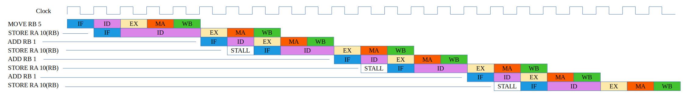

Figure 19: test case 2c, code (top), correct execution (top middle), simulation (bottom middle), actual execution (bottom)
This code would be more typical of how LOAD/STORE instructions would work, could see this block of code in a loop with RA,RB,RC and RD being pointers used to copy blocks of data stored in memory.
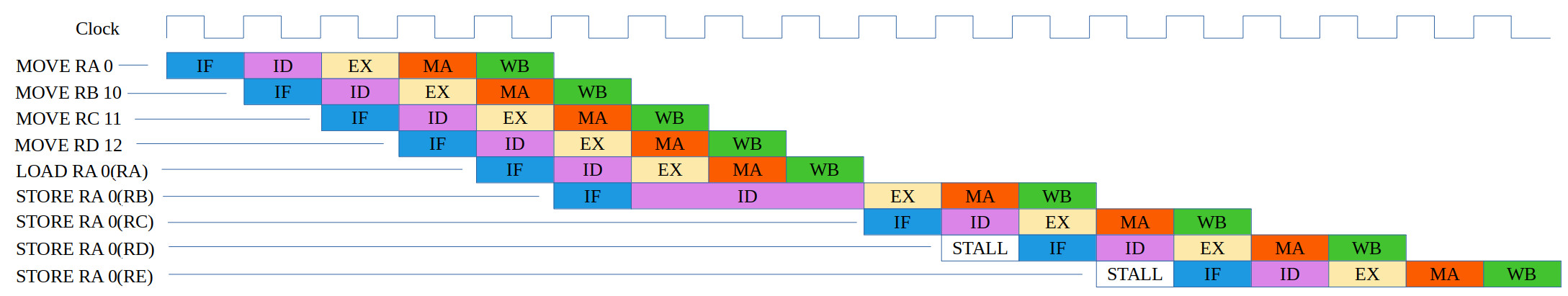

Figure 19: test case 2b, code (top), correct execution (middle), simulation (bottom)
Again this test case used to test RAW hazards i.e. does the processor what for RA - RD to be updated before performing the LOAD and STORE instructions. Also tests that structural hazards are handled correctly i.e. between the LOAD and STORE instructions.
start:
    JUMPU   skip
    MOVE RB 1

skip:
    MOVE RB 2
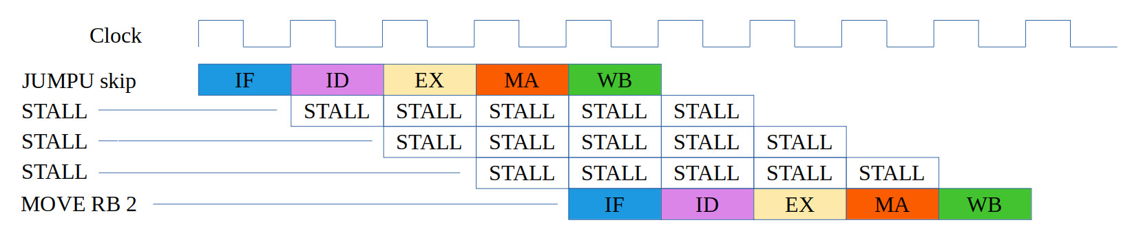
Figure 19: test case 3a, code (top), correct execution (middle), simulation (bottom)
start:
    MOVE RA 0
    MOVE RB 1
    JUMPZ RA skip1
    MOVE RC 2

skip1:
    JUMPZ RB skip2
    MOVE RC 3

skip2:
    MOVE RC 4
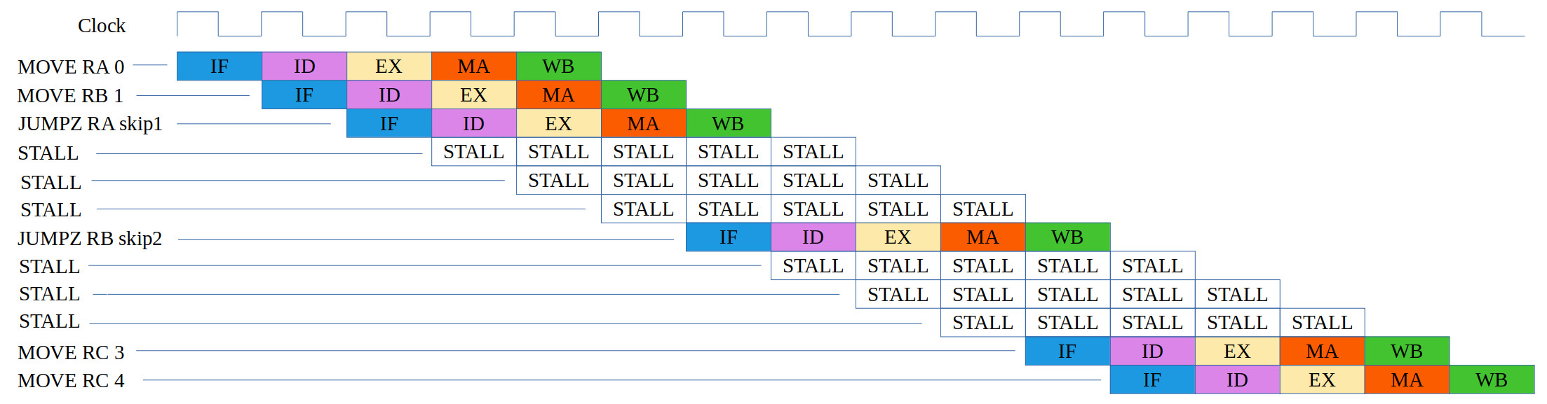
Figure 20: test case 3b, code (top), correct execution (middle), simulation (bottom)
start:
    MOVE RA 0
    MOVE RB 1
    JUMPNZ RA skip1
    MOVE RC 2

skip1:
    JUMPNZ RB skip2
    MOVE RC 3

skip2:
    MOVE RC 4
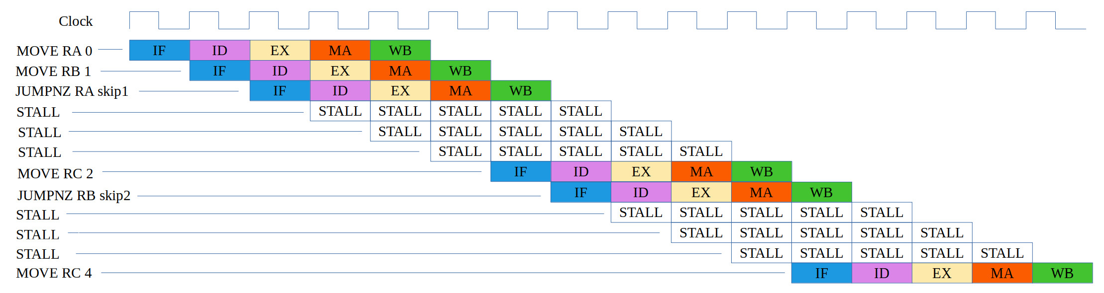

Figure 21: test case 3c, code (top), correct execution (middle), simulation (bottom)
start:
    MOVE RA 0
    JAL func
    MOVE RC 2

func:
    MOVE RC 3
    JR RH
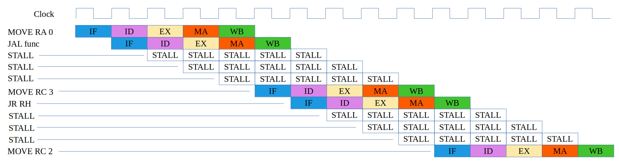

Figure 22: test case 3d, code (top), correct execution (middle), simulation (bottom)
WORK IN PROGRESS

This work is licensed under a Creative Commons Attribution-NonCommercial-NoDerivatives 4.0 International License.
Contact email: mike@simplecpudesign.com