The simpleCPU architectures are designed to be implemented on FPGA hardware (Link). The software used to implement, simulate and configure this hardware is: Xilinx ISE 14.7 (Link). This software is free and can be downloaded here: (Link). To get started on the Xilinx ISE journey below is a guide on how to install and use this software.
Software
Schematics
Simulations
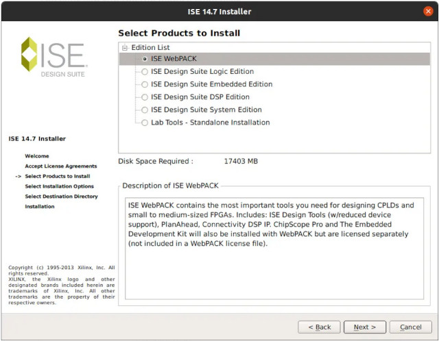
Figure 1 : ISE WebPack
To avoid reinventing the wheel, instructions on how to install the Xilinx ISE software on Windows and Linux can be accessed through the links below:
Note, before you can download the ISE software you do have to register with Xilinx, this purely for admin purposes, the WebPack version used with the simpleCPU is free i.e. the simpleCPU designs only use the basic IP cores, not the the more specialised hardware e.g. HDMI interface etc. To install the core software tools in Linux, download ISE 14.7 Full Installer for Linux from the Xilinx software download page. This is a few GBytes, so may take a while. Open a terminal and extract the TAR file, cd into the folder created and enter the commands below to start the installer:
chmod +x xsetup
sudo ./xsetup
The installer will now start, as shown in figure 1, select the ISE WebPACK option, and thats basically it. Note, cable drivers are another issue, also some of the more specialised tool in ISE do need legacy libraries, however, as we don't need these for basic schematic capture and simulations this is not a problem :).
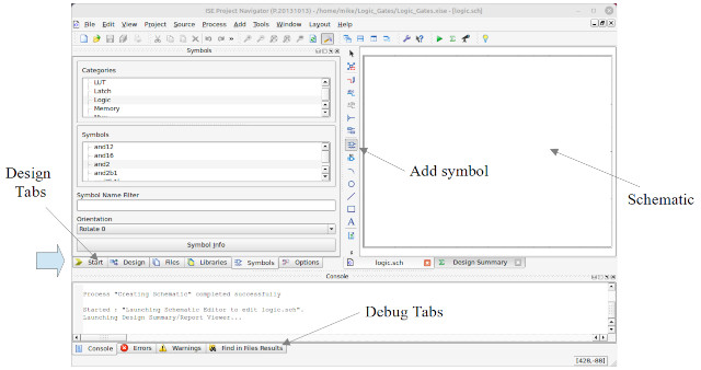
Figure 2 : ISE project navigator
To start ISE, in a terminal enter the commands below:
cd /opt/Xilinx/14.7/ISE_DS
source settings64.sh
ise
This will start the ISE project navigator, as shown in figure 2. To create a new project left click on the File pull down within the project navigator window.
File -> new project
The New project wizard will ask you to enter a name and location for this project:
Name :                  Logic_Gates
Project Location :      /home/mike/Logic_Gates
Top-level source type : Schematic
Click the Next button. Note: the software doesn't like SPACE characters in directory or file names etc, so be careful not to use them, also network drives can cause issues, so safest to stick to your home directory. You will now be asked to select the device and simulator for this project. For this test project i'm using a older Zybo board (Link), so the parameters are set to those shown below:
Family :          Zynq
Device :          XC7Z010
Package :         CLG400
Speed grade :     -3
Synthesis tools : XST (VHDL / Verilog)
Simulator :       ISim (VHDL / Verilog)
Language :        VHDL
Click the Next button. The Project navigator will now create a new project with the entered specifications. Click Finished. The required hardware needed to implement the SimpleCPU processor can be defined using schematics i.e. circuit diagrams. To create a new schematic left click on:
Project -> New Source
This will open the 'New Source Wizard', click on the Schematic Icon and enter the name and location (default project directory) for this source:
File Name : Logic
Location :  /home/mike/Logic_Gates
Click the Next button. Confirm these parameters by clicking on the Finish button. A blank schematic will appear in the main project navigator window as shown in figure 2. To add a component to the schematic click on the 'Add Symbol' icon, select its type from the Categories box e.g. Logic. This will update the Symbols design tab with the components supported by the chosen FPGA. Select the desired symbol, move the cursor onto the schematic and left click to add a component. To stop adding instances of a component press the ESC button. From the Logic component category select the INV and AND2 components, layout the schematic for this circuit, as shown in figure 3.
Tip: if you are unsure of a component’s function click on the 'Symbol Info' button at the bottom of this panel. This will open the components .pdf data sheet.
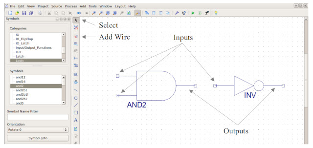
Figure 3 : Component placement
To move a component, left click on the 'Select' icon in the toolbar. Left click on the component, hold, then drag and drop (release) the component to its new position. IMPORTANT: in a schematic inputs to a circuit are placed on the left hand side and outputs on the right hand side of the circuit diagram. The two logic gates we have selected implement the logical AND and INV functions as shown in figure 4. Note, the alternative name for an INV (inverter) is a NOT gate.
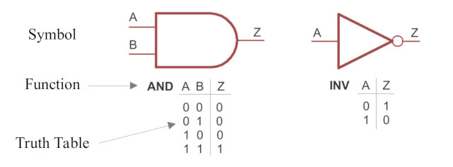
Figure 4 : Logic gates and truth tables
A logic gate processes Boolean signals, a TRUE is encoded as a logic 1 and a FALSE as a logic 0 i.e. digital signals. An INV simply outputs the opposite state to its input. An AND gate outputs a logic 1 when both its inputs are 1 i.e. A=B=1, otherwise it outputs a logic 0. A logic gates functionality is defined by its truth table. A complete set of logic gate symbols and truth tables are shown in figure 5.
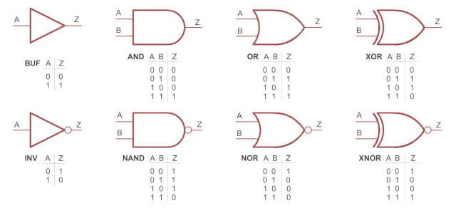
Figure 5 : Complete logic gate family
To view different parts of the schematic use the side scroll bars and the Zoom buttons shown in figure 6. Test this functionality out by zooming in on the INV gate. Tip: a quick way of doing this is to click on the 'Zoom Box' icon, position the cursor above and left of the INV gates, left click, hold, then drag and drop a box on the area to view.

Figure 6 : Zoom options
To delete a component, left click on the 'Select' icon in the toolbar. Left click on the component, then press the DEL key to remove it. To add wires (signals) click on the 'Add Wire' icon in the toolbar. Position the cursor where you would like to start, left click, hold and drag the wire to its end position e.g. an INV input. When the wire is in the correct position four small squares will appear around the cursor, release the button to place the wire, as shown in figure 7. To stop drawing wires press the ESC key.
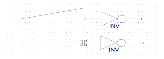
Figure 7 : Adding wires, start (top), end (bottom)
Tip: by default a wire’s path is determined automatically i.e. the path from start to finishing positions. To manually specify the path click on the 'Use Manual method' radio button within the 'Add Wire Options' panel. This is available by clicking on the Options design tab at the bottom of the left panel, shown in figure 2.
To move a wire click on the 'Select' icon, then left click, hold and drag the wire to its new position before releasing the button. Tip: by default a wire's connections to other objects are maintained e.g. the wire is stretched. To move the wire click on the 'Break connections' radio button within the Select Options panel shown in figure 8. To delete a wire or a component click on the 'Select' icon, left click on the item to select it, then press the DEL key to remove it.
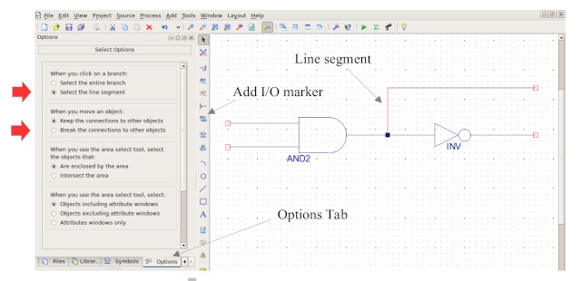
Figure 8 : Moving / deleting line (wire) segment
Tip: by default when you delete a wire the whole wire will be deleted (all wires with the same label), to delete a section of wire click on the 'Select the line segment' radio button within the Select Options panel, as shown in figure 8, the segment that would be deleted is highlighted in red. If all else fails CTRL Z will undo a lot of problems / mistakes :). Wire up the INV and AND2 components as shown in figure 8. Note, the inputs to the AND gate and the output of the INV have been extended with wires.
To assign the circuit's inputs and outputs (I/O) to the FPGA’s external pins click on the 'Add I/O Marker' icon in the toolbar. Position the cursor at the end of the selected wire, when in the correct position four small squares will appear around the cursor, left click to place the I/O pad marker. Continue wiring this circuit, placing I/O markers on all inputs and outputs, when complete your circuit diagram should be comparable to that shown in figure 9.
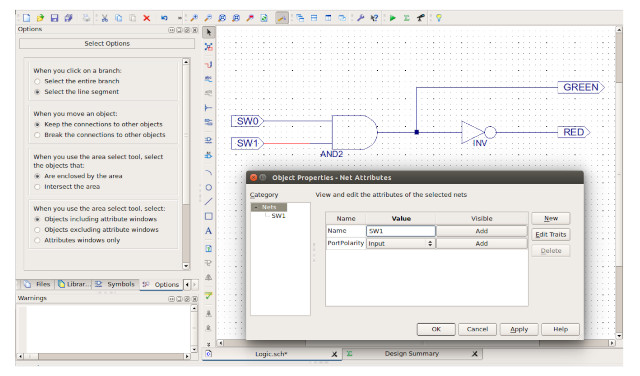
Figure 9 : logic circuit
To assign a label (name) to a wire click on the 'Select' icon, then double left click on the wire. This will open the Object Properties - 'Net Attributes' window allowing you to change the default name (Value text box) assigned to the wire. To make this label visible click on the 'Add' option, this will open the 'Net Attribute Visibility' window, showing all wires of that name. Left click on the wire (position) you wish the label to appear. Click on OK to return to the main screen. Note: if you double click on the schematic by mistake the 'Schematic Properties' box will appear, press Cancel, then reposition the cursor. You can also label an IO port by right clicking on the port, then select 'Rename Port'. When you have finished entering this circuit left click on the save icon in the top left toolbar in the main window.
A schematic's functionality can be verified before implementation using a hardware simulator. To specify what input signals (test cases) should be applied to the Unit Under Test (UUT) a VHDL (Link) test bench must be created. Left click on:
Project -> New Source
This will open the 'New Source Wizard', click on the VHDL Test Bench Icon and enter the name and location (default project directory) for this source:
File Name : Logic_TB
Location : /home/mike/Logic_Gates
Click the Next button. Click Next again to associated this file with the schematic Logic. Confirm these parameters by clicking on the Finish button. This will generate a VHDL test bench template i.e. no test case is defined, just the UUT. Edit the VHDL test bench template to match figure 10. This defines the series of tests that we want to perform, you can download a copy here: (Link). Note: some lines in the template are dependent on the order the various wires were added to the schematic, this will not affect how the simulation will function.
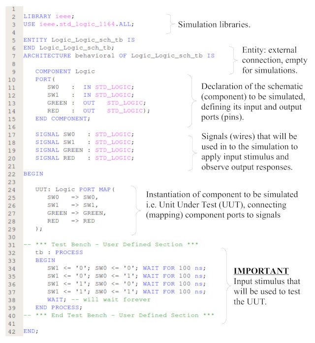
Figure 10 : VHDL testbench
Left click on the Design tab (figure 2, bottom left) to display project sources. Click on the Simulation radio button, then within the pull down box (top left) ensure Behavioral simulation is selected, as shown in figure 11. Left click (highlight) on the testbench file Logic_TB, this will update the Processes for source window, then double left click on Simulate Behavioural Model. IMPORTANT: you must select the testbench file before you launch the simulator i.e. the file ending with "_TB", as the software will allow you to simulate any file, even if it can't be simulated. If you do make this mistake the waveform will be ORANGE / RED rather than GREEN.
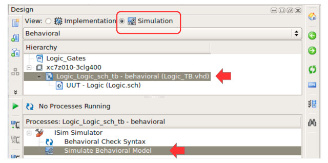
Figure 11 : Simulating a schematic
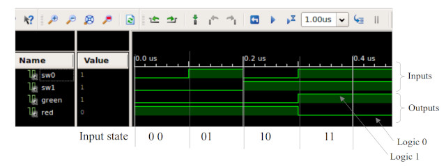
Figure 12 : Functional timing waveform diagram
The VHDL simulator allows the operation of the circuit to be checked by examining its waveform timing diagram i.e. comparing the simulated outputs to those in its original truth table, as shown in figure 12. Tip, you may have to rescale the waveform diagram to fit the display window. This can be achieved by clicking on the magnifying glass icon in the top left corner of the ISim window. In this simulation all possible input states (logic values) are applied to the unit under test (UUT) i.e. the INV and AND2 components, via the signals SW1 and SW0. The results of this simulation can be verified by observing the state of the outputs signals GREEN and RED during each input state i.e. GREEN=AND, RED=NAND.
The waveform diagram shown is a functional simulation i.e. no routing or logic delays are included. This can be confirmed by examining the timing relationship between changes on inputs SW_1 or SW_0 and the outputs GREEN and RED. In a real systems these instantaneous changes would not be possible i.e. it will take some time (ns) for an electrical signal to travel down a wire or through the transistors in the logic gates before an output is updated i.e. signals would not change at the same time.
Note: functional simulation lack information regarding logic and routing delays which may be important when determining how a circuit will perform in a real world e.g. determining the critical path delay (CPD), which we will be looking at later. The Xilinx ISE software does allow more detailed simulations to be performed, however, these would take significantly longer to run. However, for the purposes of understanding how the simpleCPU works functional simulations are fine, but do remember they are only an approximation.
The final step would be to upload this design into an FGPA and test it functions correctly, however, you would need the hardware to do this :)
WORK IN PROGRESS

This work is licensed under a Creative Commons Attribution-NonCommercial-NoDerivatives 4.0 International License.
Contact email: mike@simplecpudesign.com