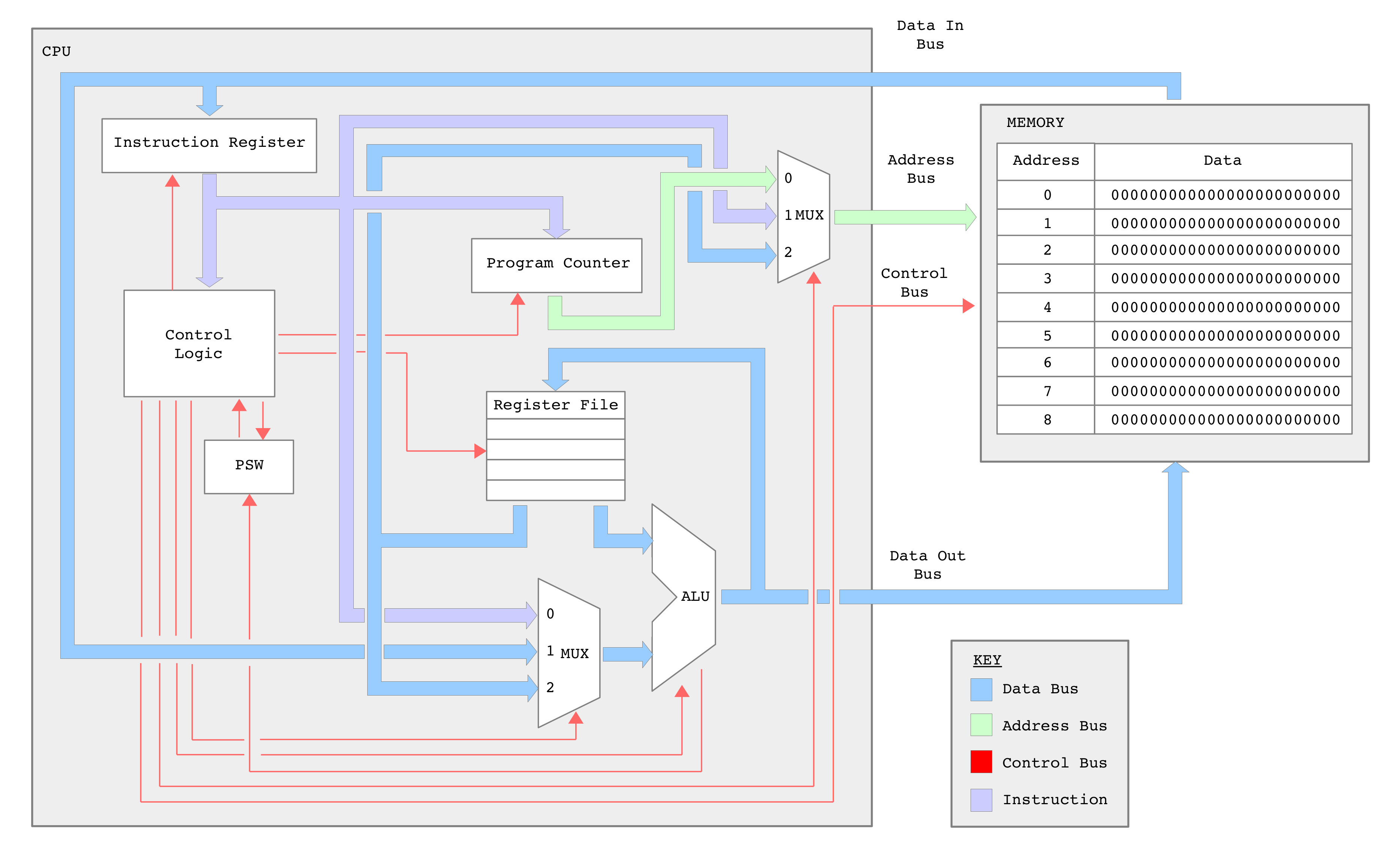
Figure 1 : simpleCPU_v1dv2 block diagram, spot the differences
##################################
# SIMPLECPU V1D2 INSTRUCTION-SET #
##################################

INSTR   IR15 IR14 IR13 IR12 IR11 IR10 IR09 IR08 IR07 IR06 IR05 IR04 IR03 IR02 IR01 IR00
MOVE    0    0    0    0    RD   RD   0    0    K    K    K    K    K    K    K    K
MOVEH   0    0    0    0    RD   RD   0    1    K    K    K    K    K    K    K    K
MOVEU   0    0    0    0    RD   RD   1    0    K    K    K    K    K    K    K    K

ADD     0    0    0    1    RD   RD   0    0    K    K    K    K    K    K    K    K
ADDU    0    0    0    1    RD   RD   0    1    K    K    K    K    K    K    K    K
ADDC    0    0    0    1    RD   RD   1    0    K    K    K    K    K    K    K    K
SUB     0    0    1    0    RD   RD   0    0    K    K    K    K    K    K    K    K
SUBU    0    0    1    0    RD   RD   0    1    K    K    K    K    K    K    K    K
SUBC    0    0    1    0    RD   RD   0    1    K    K    K    K    K    K    K    K

AND     0    0    1    1    RD   RD   0    0    K    K    K    K    K    K    K    K
OR      0    0    1    1    RD   RD   0    1    K    K    K    K    K    K    K    K
XOR     0    0    1    1    RD   RD   1    0    K    K    K    K    K    K    K    K

LOAD    0    1    0    0    A    A    A    A    A    A    A    A    A    A    A    A
STORE   0    1    0    1    A    A    A    A    A    A    A    A    A    A    A    A
ADDM    0    1    1    0    A    A    A    A    A    A    A    A    A    A    A    A
SUBM    0    1    1    1    A    A    A    A    A    A    A    A    A    A    A    A

JUMPU   1    0    0    0    A    A    A    A    A    A    A    A    A    A    A    A
JUMPZ   1    0    0    1    0    0    0    R    R    R    R    R    R    R    R    R  -- RELATIVE -256 to +255
JUMPNZ  1    0    0    1    0    0    1    R    R    R    R    R    R    R    R    R
JUMPC   1    0    0    1    0    1    0    R    R    R    R    R    R    R    R    R
JUMPNC  1    0    0    1    0    1    1    R    R    R    R    R    R    R    R    R
JUMPO   1    0    0    1    1    0    0    R    R    R    R    R    R    R    R    R
JUMPNO  1    0    0    1    1    0    1    R    R    R    R    R    R    R    R    R
JUMPN   1    0    0    1    1    1    0    R    R    R    R    R    R    R    R    R
JUMPP   1    0    0    1    1    1    1    R    R    R    R    R    R    R    R    R

CMP     1    0    1    0    RD   RD   0    0    K    K    K    K    K    K    K    K
TEST    1    0    1    0    RD   RD   0    1    K    K    K    K    K    K    K    K
MULU    1    0    1    1    RD   RD   X    X    K    K    K    K    K    K    K    K

ADDMC   1    1    0    0    A    A    A    A    A    A    A    A    A    A    A    A
SUBMC   1    1    0    1    A    A    A    A    A    A    A    A    A    A    A    A

CALL    1    1    1    0    A    A    A    A    A    A    A    A    A    A    A    A
RET     1    1    1    1    X    X    X    X    X    X    X    0    0    0    0    0

MOVE    1    1    1    1    RD   RD   RS   RS   X    X    X    0    0    0    0    1
LOAD    1    1    1    1    RD   RD   RS   RS   X    X    X    0    0    0    1    0  -- REG INDIRECT
STORE   1    1    1    1    RD   RD   RS   RS   X    X    X    0    0    0    1    1  -- REG INDIRECT
ROL     1    1    1    1    RSD  RSD  X    X    X    X    X    0    0    1    0    0
ROR     1    1    1    1    RSD  RSD  X    X    X    X    X    0    0    1    0    1

ADD     1    1    1    1    RD   RD   RS   RS   X    X    X    0    0    1    1    0
SUB     1    1    1    1    RD   RD   RS   RS   X    X    X    0    0    1    1    1
AND     1    1    1    1    RD   RD   RS   RS   X    X    X    0    1    0    0    0
OR      1    1    1    1    RD   RD   RS   RS   X    X    X    0    1    0    0    1
XOR     1    1    1    1    RD   RD   RS   RS   X    X    X    0    1    0    1    0
ASL     1    1    1    1    RSD  RSD  X    X    X    X    X    0    1    0    1    1
ASR     1    1    1    1    RSD  RSD  X    X    X    X    X    0    1    1    0    0
SHL     1    1    1    1    RD   RD   X    X    X    X    X    0    1    1    0    1
SHR     1    1    1    1    RD   RD   X    X    X    X    X    0    1    1    1    0

ADDC    1    1    1    1    RD   RD   RS   RS   X    X    X    0    1    1    1    1
SUBC    1    1    1    1    RD   RD   RS   RS   X    X    X    1    0    0    0    0
CMP     1    1    1    1    RD   RD   RS   RS   X    X    X    1    0    0    0    1
TEST    1    1    1    1    RD   RD   RS   RS   X    X    X    1    0    0    1    0
MULU    1    1    1    1    RD   RD   RS   RS   X    X    X    1    0    0    1    1
Another year, another processor :). When designing the simpleCPU processor the goal was not to build the fastest processor, the best processor i.e. a replacement for an off the shelf processor, that could be purchased for a fraction of the cost, rather it was to build a processor that would be used for teaching. There are a lot of different approaches to teaching computer architectures and i'm sure many of my colleagues would disagree with the way i run the SYS1 module, but for me learning is something you do by doing, something that a student has to actively engage with. Therefore, for me learning is something a student has to experience, simply using a "thing" is not enough, you need to build that "thing", fail to get the "thing" to do what you want it to do and have to build a new "thing". This work also needs to be set in a real world context to understand why that "thing" looks the way it does, you need to become the "thing" (Link) :). Soooo the simpleCPU processor is a platform from which a student can experience what a processor is, something they can build upon, add features and functionality to, a platform where they can experience what works and what does not, go beyond simply using a processor. Well that is the thought :).
From figure 1 you should spot that there are no top level architectural changes from the simpleCPUv1d to the simpleCPUv1d2. I did consider adding more general purpose data registers, different data paths, but these are "nice to have" improvements, rather than "teaching" improvements. Not to say there isn't significant changes to some of these hardware components, but these changes are driven by changes to the instruction-set i.e. to add more instructions, to add more flexibility to the processor, to make it easier to use, easier to program.
The new and improved ISE project files for this processor can be downloaded here: (Link). Note, this is a work in progress, i update periodically so may not be the latest and greatest, there may also be features / bugs :).
Improvement 1 : immediate addressing mode
Improvement 2 : changes to data MUX
Improvement 3 : AND, OR, XOR instructions
Improvement 4 : relative addressing mode
Improvement 5 : changes to the PC
Improvement 6 : ROL, ROR, ASL, ASR, SHR and SHL instructions
Improvement 7 : CMP and TEST instructions
Improvement 8 : MULU instruction
Improvement 9 : ADDC, ADDMC, SUBC, SUBMC instructions
Testing : simulating the new instructions
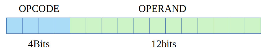
Figure 2 : basic instruction format
A basic simpleCPU instruction is a 16bit fixed length instruction, with a 4bit opcode and a 12bit operand. To add more flexibility and functionality i could switch to a variable length instruction format e.g. instruction could vary in size, from 8bit to 64bit+ in length, depending on their requirements / operands etc. You can see an example of this type of micro-coded architecture in the simpleCPUv2 (Link). However, this approach significantly increases the complexity of the fetch-phase and control logic, therefore, making it more difficult for students to add new instructions. So i decided to stick with fixed length instructions. The downside of this is that you are limited to 16 basic instructions, which is enough to make a simple processor i.e. the simpleCPUv1a (Link), but its a little limited. That is, the ideal teaching processor should NOT do everything a student whats i.e. some of those features are for the student to add, but equally it should not cause excessive frustration when programming like the minimalCPU :) (Link). Fortunately, there is space within the existing instructions to add additional bit-fields, to expand the functionality of some of the instructions. Consider the immediate addressing mode instruction format shown in figure 3.
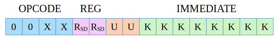
Figure 3 : immediate addressing mode instruction format
# INSTR   IR15 IR14 IR13 IR12 IR11 IR10 IR09 IR08 IR07 IR06 IR05 IR04 IR03 IR02 IR01 IR00

# MOVE    0    0    0    0    RD   RD   U    U    K    K    K    K    K    K    K    K
# ADD     0    0    0    1    RD   RD   U    U    K    K    K    K    K    K    K    K
# SUB     0    0    1    0    RD   RD   U    U    K    K    K    K    K    K    K    K
# AND     0    0    1    1    RD   RD   U    U    K    K    K    K    K    K    K    K
All immediate addressing mode instruction opcodes start with 00, have a 2bit register select field and an 8bit immediate value. They also have two unused bits (UU). Therefore, these bits can be used to augment the functionality of these instructions. Thats is, where possible, without significant changes to the processor's hardware we can use these bits to add new instructions. Note, i'm not looking to just add instructions here, rather expand the functionality of the existing ones, any changes should not break existing instructions, the instruction must use the same addressing mode, or at a push be a variation upon. Looking to show how we can expand the processor's instruction-set, rather than rewrite from scratch.
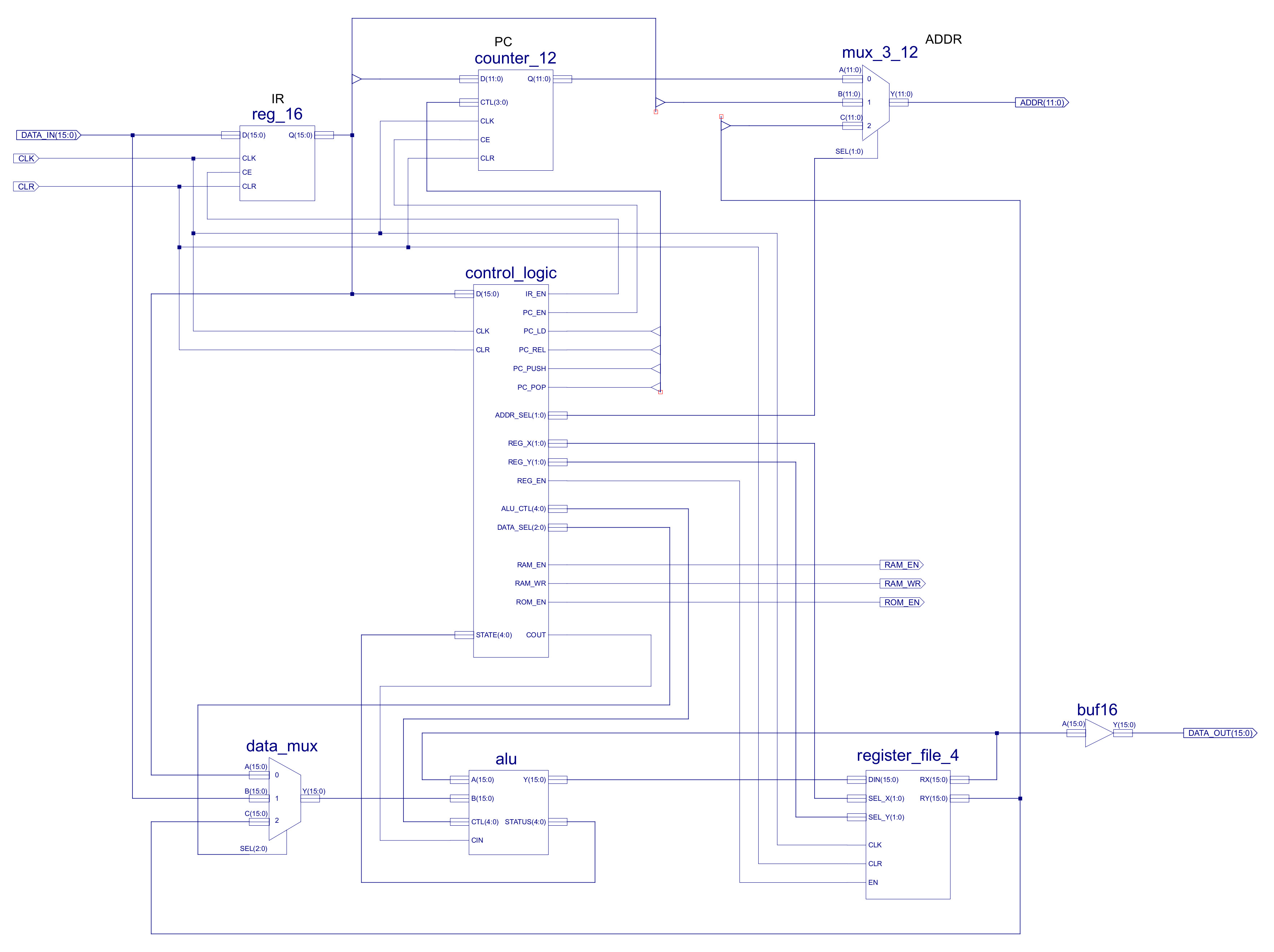
Figure 4 : simpleCPUv1d2 top level schematic
The top level schematic of the simpleCPUv1d2 is shown in figure 4, from this we can identify the possible data paths for the immediate addressing mode. This hardware is fixed, partially to maintain consistency with the previous version, but to also help ensure we meet timing closure i.e. we don't change the critical path delay tooo much. Sooo the first improvement is to add new MOVE instructions:
INSTR   IR15 IR14 IR13 IR12 IR11 IR10 IR09 IR08 IR07 IR06 IR05 IR04 IR03 IR02 IR01 IR00

MOVE    0    0    0    0    RD   RD   0    0    K    K    K    K    K    K    K    K
MOVEH   0    0    0    0    RD   RD   0    1    K    K    K    K    K    K    K    K
MOVEU   0    0    0    0    RD   RD   1    0    K    K    K    K    K    K    K    K

Example          :    move RA 0xFF, RA = 0xFFFF
Addressing mode  :    immediate
Opcode           :    0000 00
RTL              :    RX <- ( (K7)8 || KK )
Flags set        :    None
Description      :    write 8bit immediate value to low byte position and sign extend high byte

Example          :    moveh RA 0xFF, RA = 0xFF00
Addressing mode  :    immediate
Opcode           :    0000 01
RTL              :    RX <- ( KK || 00 )
Flags set        :    None
Description      :    write 8bit immediate value to high byte position

Example          :    moveu RA 1, RA = 0x00FF
Addressing mode  :    immediate
Opcode           :    0000 10
RTL              :    RX <- ( 00 || KK )
Flags set        :    None
Description      :    write 8bit immediate value to low byte position and zero high byte
MOVE is a signed extended 8bit move, MOVEH is a write 8bit immediate to high byte position, low byte is zeroed. MOVEU is an unsigned move, write 8bit immediate into low byte position, high byte zeroed. These changes help support the use of unsigned values e.g. loop counter, you don't always need a signed value :), Also the generation of 16bit data values in code i.e. how do you set a variable to a 16bit value when your immediate bit-field is limited to an 8bit value. Answer: MOVEH + OR.
I have implemented most of the ADD and SUB instructions, did need to make some changes to the ALU's adder/subtractor to allow me to add instructions to include the previous carry flag values, to allow the addition of values greater than 16bits i.e. numbers spread across multiple memory locations, 32bits values. However, as all my webpages state "This is work in process" :), the instructions now include :
INSTR   IR15 IR14 IR13 IR12 IR11 IR10 IR09 IR08 IR07 IR06 IR05 IR04 IR03 IR02 IR01 IR00

ADD     0    0    0    1    RD   RD   0    0    K    K    K    K    K    K    K    K
ADDU    0    0    0    1    RD   RD   0    1    K    K    K    K    K    K    K    K
ADDC    0    0    0    1    RD   RD   1    0    K    K    K    K    K    K    K    K

SUB     0    0    1    0    RD   RD   0    0    K    K    K    K    K    K    K    K
SUBU    0    0    1    0    RD   RD   0    1    K    K    K    K    K    K    K    K
SUBC    0    0    1    0    RD   RD   1    0    K    K    K    K    K    K    K    K

Example            :    add RB 2
Addressing mode    :    immediate
Opcode             :    0001 00
RTL                :    RX <- RX + ( (K7)8 || KK )
Flags set          :    Z,C,O,P,N
Description        :    signed addition

Example            :    addu RB 2
Addressing mode    :    immediate
Opcode             :    0001 01
RTL                :    RX <- RX + ( 00 || KK )
Flags set          :    Z,C,O,P,N
Description        :    unsigned addition

Example            :    addc RB 2
Addressing mode    :    immediate
Opcode             :    0001 10
RTL                :    RX <- RX + ( (K7)8 || KK ) + carry flag
Flags set          :    Z,C,O,P,N
Description        :    signed addition + cary flag

Example            :    sub RB 2
Addressing mode    :    immediate
Opcode             :    0010 00
RTL                :    RX <- RX - ( (K7)8 || KK )
Flags set          :    Z,C,O,P,N
Description        :    signed subtraction

Example            :    subu RB 2
Addressing mode    :    immediate
Opcode             :    0010 01
RTL                :    RX <- RX + ( 00 || KK )
Flags set          :    Z,C,O,P,N
Description        :    unsigned subtraction

Example            :    subc RB 2
Addressing mode    :    immediate
Opcode             :    0010 10
RTL                :    RX <- RX - ( (K7)8 || KK ) - carry flag
Flags set          :    Z,C,O,P,N
Description        :    signed subtraction - carry flag
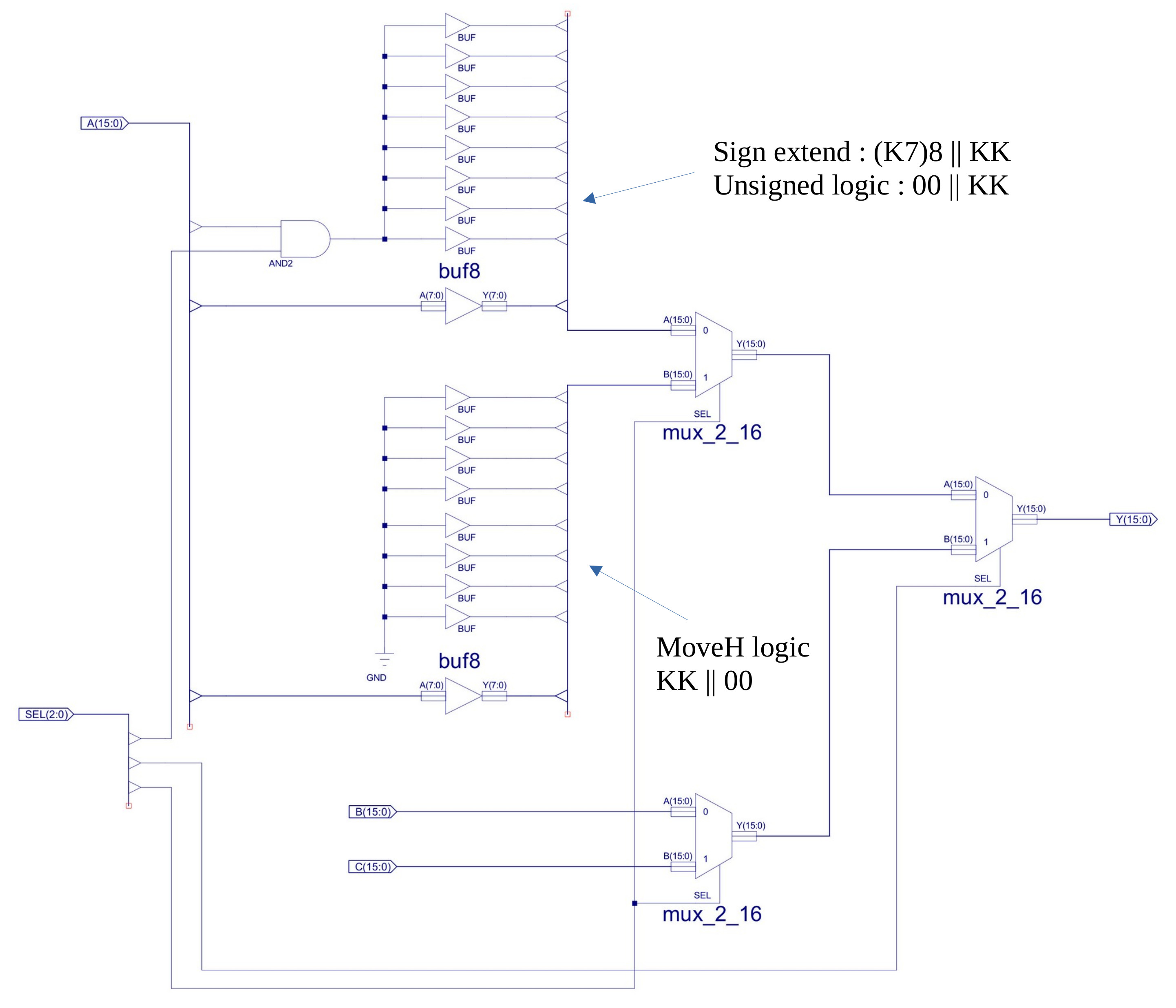
Figure 5 : changes to data MUX
To allow the different MOVE instructions to function we need to update the DATA_MUX component shown in figure 5. This multiplexer always did have an unused A-input branch that was included for future addressing mode expansion, which i confess i never got around to adding until now :). Sooo this hardware was removed and the hardware needed for the MOVEH instruction added. The top A-input logic generates sign extended and unsigned immediate values. The bottom A-input logic generates the MOVEH value, writing the immediate value to the high byte of the destination register and zeroing the low byte.
To implement the Boolean logic functions the AND_16, OR_16 and XOR_16 components have been added to the ALU, as shown in figure 6. These components are just an array of 16 2-input logic gates that perform the required bit-wise operations i.e. exactly the same as the previous bitwise AND component just using OR and XOR. For these changes i am slightly pushing the limits of the rules i set, but rather than implementing different types of AND instructions, i decided to go for a Boolean instruction group by adding support for bitwise OR and XOR using an opcode modifier in bits 8 and 9:
INSTR   IR15 IR14 IR13 IR12 IR11 IR10 IR09 IR08 IR07 IR06 IR05 IR04 IR03 IR02 IR01 IR00

AND     0    0    1    1    RD   RD   0    0    K    K    K    K    K    K    K    K
OR      0    0    1    1    RD   RD   0    1    K    K    K    K    K    K    K    K
XOR     0    0    1    1    RD   RD   1    0    K    K    K    K    K    K    K    K

Example            :    and RD 0x04
Addressing mode    :    immediate
Opcode             :    0011 00
RTL                :    RX <- RX & ( (0)8 || KK )
Flags set          :    Z,C,O,P,N
Description        :    bitwise AND of immediate 8bit values and low byte of register

Example            :    or RD 0x04
Addressing mode    :    immediate
Opcode             :    0011 01
RTL                :    RX <- RX | ( (0)8 || KK )
Flags set          :    None
Note               :    bitwise OR of immediate 8bit values and low byte of register

Example            :    xor RD 0x04
Addressing mode    :    immediate
Opcode             :    0011 10
RTL                :    RX <- RX ^ ( (0)8 || KK )
Flags set          :    None
Note               :    bitwise XOR of immediate 8bit values and low byte of register
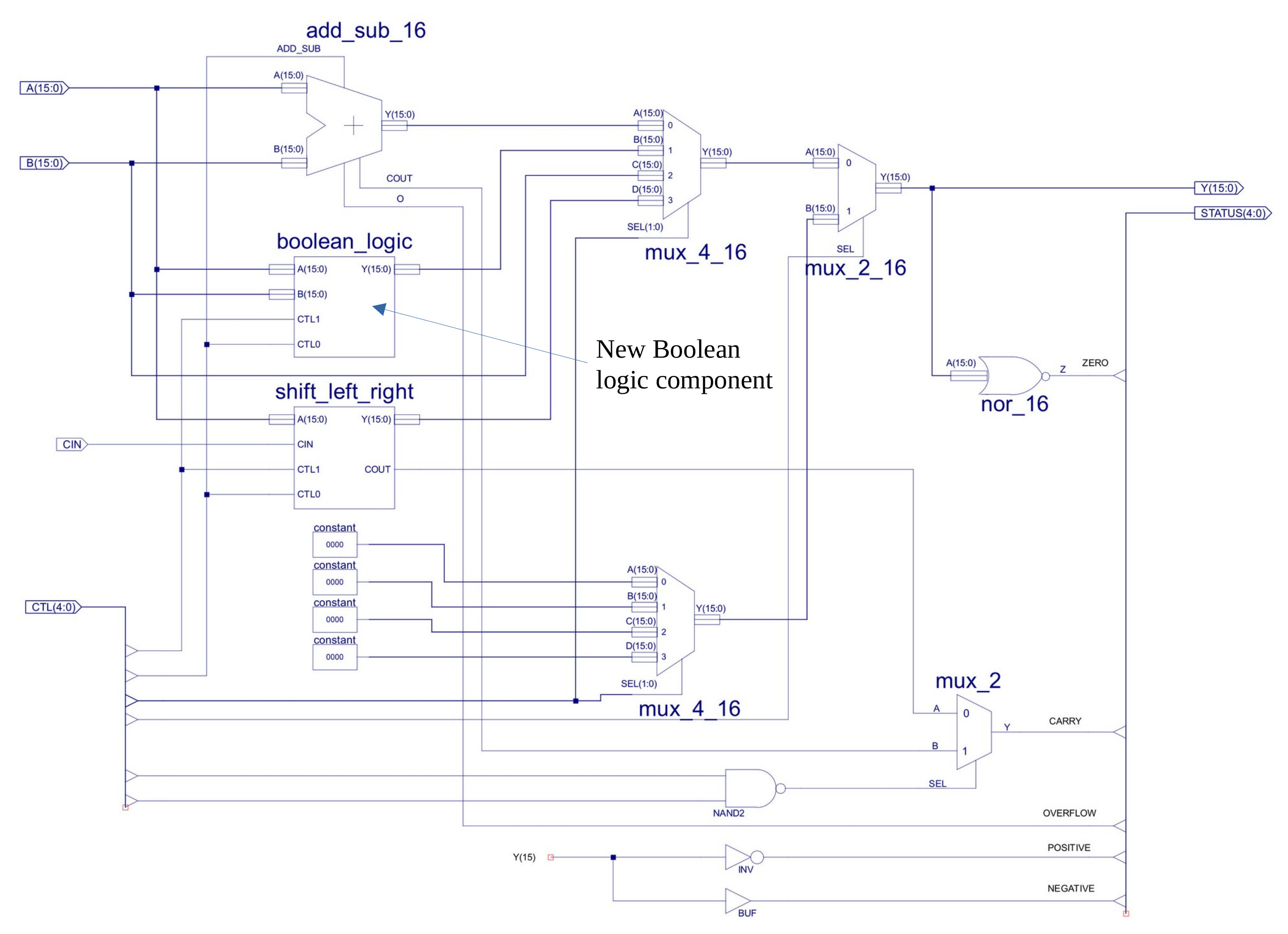
Figure 6 : ALU
The simpleCPU has four JUMP instructions (listed below), one unconditional and three conditional jumps. These use the absolute/direct addressing mode i.e. they contain the 12bit branch target address.
INSTR   IR15 IR14 IR13 IR12 IR11 IR10 IR09 IR08 IR07 IR06 IR05 IR04 IR03 IR02 IR01 IR00

JUMPU   1    0    0    0    A    A    A    A    A    A    A    A    A    A    A    A
JUMPZ   1    0    0    1    A    A    A    A    A    A    A    A    A    A    A    A
JUMPNZ  1    0    1    0    A    A    A    A    A    A    A    A    A    A    A    A
JUMPC   1    0    1    1    A    A    A    A    A    A    A    A    A    A    A    A
Note, for the simpleCPU i slightly bend the definitions of absolute and direct addressing modes, so that i can differentiate between addresses used in LOAD/STORE instructions and those used in JUMP instructions. If the specified address points to a data value, in the simpleCPU i refer to this as an absolute addressing mode. If the specified address points to an instruction, in the simpleCPU i refer to this as an direct addressing mode. Both absolute/direct addressing modes are addresses, its just that i think its useful to highlight what these instructions are pointing to different "things". For people that don't like this, all i can say is its my processor, so my rules :)
The downside of the implementation in the simpleCPUv1d is that these four JUMP instructions take 4 of the 16 base opcode values, is this a big chunk of opcodes, limiting the processor's istruction-set. Also, to simplify coding, to improve code density we need to increase the number of conditional JUMP instructions, however, there are no spare opcodes to do this :(. Sooo, to make some space we can take advantage of the observation that the branch target address distance of a conditional jump is small, we rarely need to branch the full address range, typically we only need to skip forwards or backwards a few instructions i.e. a small relative jump. Therefore, rather than specifying the branch-target address as an absolute/direct address we can use a relative address i.e. an +/- offset from the current PC value. Using this approach we now have bit-fields free to define a range of conditional jump instructions:
INSTR   IR15 IR14 IR13 IR12 IR11 IR10 IR09 IR08 IR07 IR06 IR05 IR04 IR03 IR02 IR01 IR00
# JUMPU   1    0    0    0    A    A    A    A    A    A    A    A    A    A    A    A     Absolute addressing mode
# JUMPZ   1    0    0    1    0    0    0    R    R    R    R    R    R    R    R    R     Relative addressing mode
# JUMPNZ  1    0    0    1    0    0    1    R    R    R    R    R    R    R    R    R     Relative addressing mode
# JUMPC   1    0    0    1    0    1    0    R    R    R    R    R    R    R    R    R     Relative addressing mode
# JUMPNC  1    0    0    1    0    1    1    R    R    R    R    R    R    R    R    R     Relative addressing mode
# JUMPO   1    0    0    1    1    0    0    R    R    R    R    R    R    R    R    R     Relative addressing mode
# JUMPNO  1    0    0    1    1    0    1    R    R    R    R    R    R    R    R    R     Relative addressing mode
# JUMPN   1    0    0    1    1    1    0    R    R    R    R    R    R    R    R    R     Relative addressing mode
# JUMPP   1    0    0    1    1    1    1    R    R    R    R    R    R    R    R    R     Relative addressing mode

Example            :    jump 200
Addressing mode    :    direct
Opcode             :    1000
RTL                :    PC <- AAA
Flags set          :    None
Description        :    unconditional jump, 12bit absolute address

Example            :    jumpz 201
Addressing mode    :    direct
Opcode             :    1001 000
RTL                :    IF Z=1 THEN PC <- PC + RRR ELSE PC <- PC + 1
Flags set          :    None
Description        :    jump if zero conditional jump, signed 9bit relative address, jump if last
                        arithmetic / logical instruction generated a zero result.

Example            :    jumpnz 202
Addressing mode    :    direct
Opcode             :    1001 001
RTL                :    IF Z=0 THEN PC <- PC + RRR ELSE PC <- PC + 1
Flags set          :    None
Description        :    jump if not zero conditional jump, signed 9bit relative address, jump if last
                        arithmetic / logical instruction did not generate a zero result.

Example            :    jumpc 203
Addressing mode    :    direct
Opcode             :    1001 010
RTL                :    IF C=1 THEN PC <- PC + RRR ELSE PC <- PC + 1
Flags set          :    None
Description        :    jump if carry conditional jump, signed 9bit relative address, jump if last
                        arithmetic / logical instruction generated a carry.

Example            :    jumpnc 204
Addressing mode    :    direct
Opcode             :    1001 011
RTL                :    IF C=0 THEN PC <- PC + RRR ELSE PC <- PC + 1
Flags set          :    None
Description        :    jump if not carry conditional jump, signed 9bit relative address, jump if last
                        arithmetic / logical instruction did not generate a carry.

Example            :    jumpo 205
Addressing mode    :    direct
Opcode             :    1001 100
RTL                :    IF O=1 THEN PC <- PC + RRR ELSE PC <- PC + 1
Flags set          :    None
Description        :    jump if overflow conditional jump, signed 9bit relative address, jump if last
                        arithmetic / logical instruction generated an overflow.

Example            :    jumpno 206
Addressing mode    :    direct
Opcode             :    1001 101
RTL                :    IF O=0 THEN PC <- PC + RRR ELSE PC <- PC + 1
Flags set          :    None
Description        :    jump if not overflow conditional jump, signed 9bit relative address, jump if last
                        arithmetic / logical instruction did not generate an overflow.

Example            :    jumpn 207
Addressing mode    :    direct
Opcode             :    1001 110
RTL                :    IF N=1 THEN PC <- PC + RRR ELSE PC <- PC + 1
Flags set          :    None
Description        :    jump if negative conditional jump, signed 9bit relative address, jump if last
                        arithmetic / logical instruction generated a negative result.

Example            :    jumpp 208
Addressing mode    :    direct
Opcode             :    1001 111
RTL                :    IF P=1 THEN PC <- PC + RRR ELSE PC <- PC + 1
Flags set          :    None
Description        :    jump if positive conditional jump, signed 9bit relative address, jump if last
                        arithmetic / logical instruction generated a positive result.
Unconditional JUMP/CALL use a 12bit absolute/direct address (AAA) allowing them to traverse the full address range. Conditional jumps use a signed 9bit relative address (RRR) i.e. PC-256 to PC+255. Note, assembler detects if relative jump distance exceeded and flags an error.
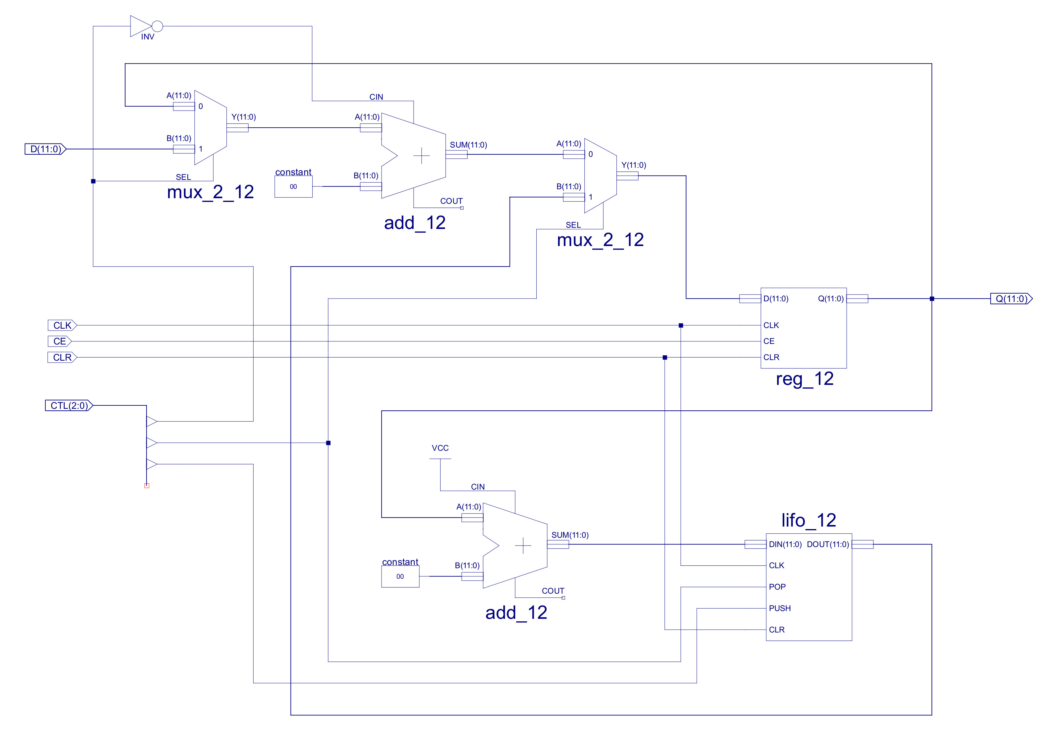
Figure 7 : original PC
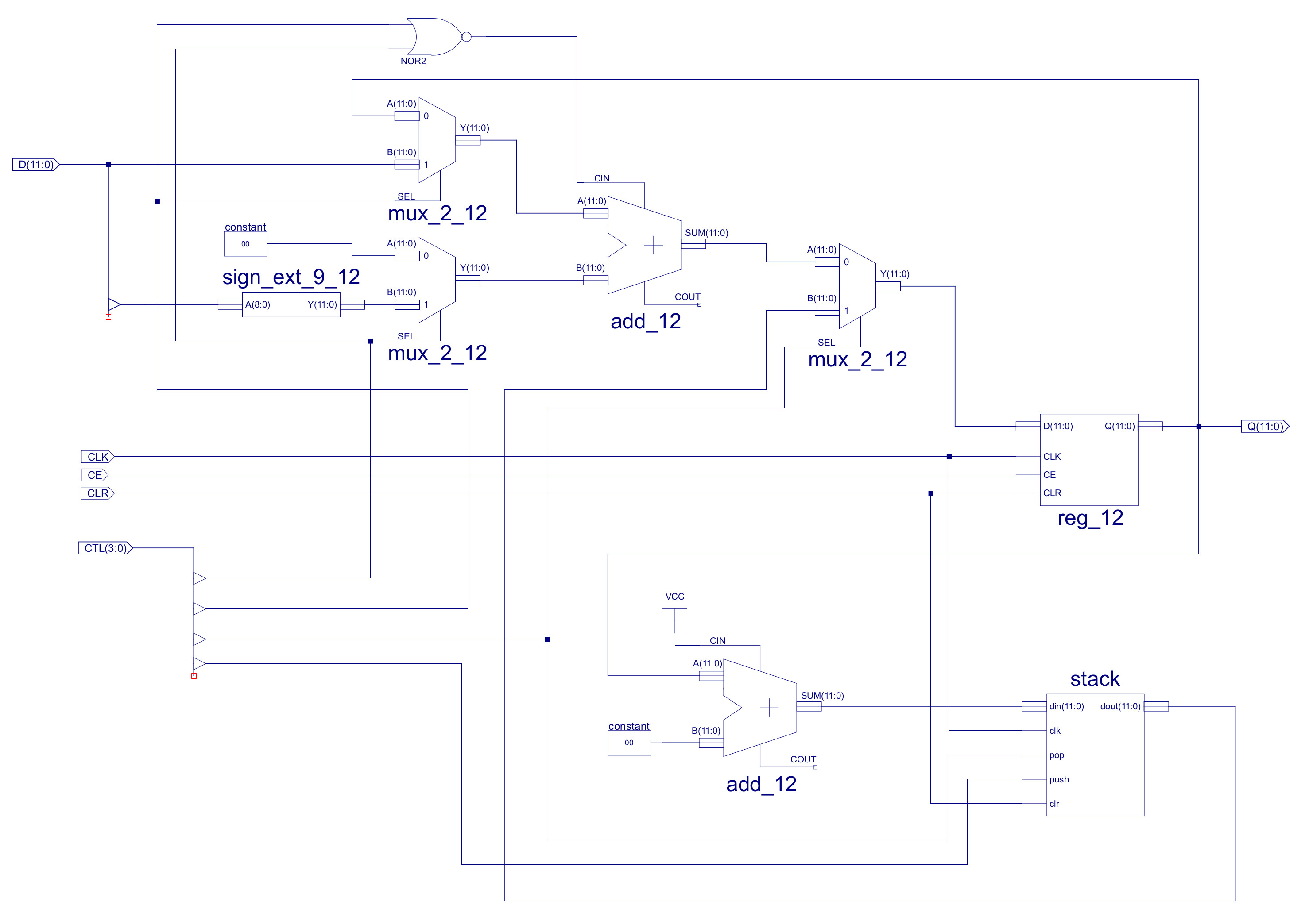
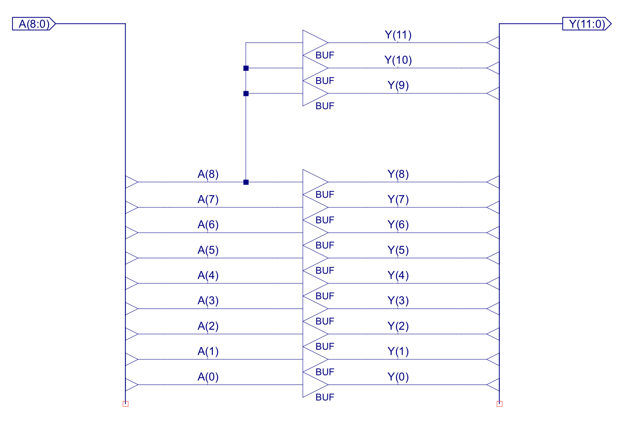
Figure 8 : changes to the PC (top), 9-to-12bit sign extender logic (bottom)
To implement the relative addressing mode we need to update the program counter (PC) component, as shown in figures 7 and 8. As you can see i have added a second multiplexer on the B input of the top adder. This allows the control logic to add a sign extended 9bit immediate stored in the JUMP instruction to the PC i.e. the PC can be updated within the range PC-256 to PC+255. These muxs are controlled by control signals CTL3 and CTL0:
CTL3  CTL0   MUX_A_OUT   MUX_B_OUT    CIN    ADDER_OUT
0     0        PC           0         1        PC+1
0     1        ABS          0         0        ABS
1     0        PC           REL       0        PC+REL
1     1        ABS          REL       0        NOT-USED
The second update to the PC is to the CALL/RET stack. In the original PC the LIFO stack was implemented as a schematic, a register based stack with a depth of 4. However, after using this in a number of different applications i found a call depth of 4 a little limiting, sooo i increased the call depth to 8, which was a lot more usable i.e. when using subroutine it was very easily to miss that you have had exceeded the call depth of 4, that you had overwritten the return addresses. As you can imagine when this did occur you would observe very "interesting" behaviours. Note, moving to a call depth of 8 does not remove this issue, just makes its less likely, sooo always keep an eye on what subroutines are calling other subroutines. To do this i normally have the stack-pointer as a trace on my waveform simulation, when things go mad this is the fist thing i check :).
Figure 9 : new LILO_12
Figure 10 : rotate_shift_left component
Figure 11 : ALU carry flag multiplexers
The logic to implement the shift left / right function is simply buffers i.e. wires, implementing a fixed shift. To fill the bubble, multiplexers are used to select between a fixed 0 for ASL and ASR, and the carry flag (C) for SHR and SHL and the "lost" bit for ROL and ROR. The new rotate_shift_left component is shown in figure 10, the rotate_shift_right is basically the same, just with the buffers wired to perform a shift right. The ALU now also needs extra MUXs to select the carry out source i.e. from the shift logic, or the adder/subtractor, as shown in figure 11. Note, did consider a barrel shifter, but wanted to keep the hardware small. As always its a trade-off between code size and hardware size.
INSTR   IR15 IR14 IR13 IR12 IR11 IR10 IR09 IR08 IR07 IR06 IR05 IR04 IR03 IR02 IR01 IR00
ROL     1    1    1    1    RSD  RSD  X    X    X    X    X    0    0    1    0    0
ROR     1    1    1    1    RSD  RSD  X    X    X    X    X    0    0    1    0    1
ASL     1    1    1    1    RSD  RSD  X    X    X    X    X    0    1    0    1    1
ASR     1    1    1    1    RSD  RSD  X    X    X    X    X    0    1    1    0    0
SHL     1    1    1    1    RSD  RSD  X    X    X    X    X    0    1    1    0    1
SHR     1    1    1    1    RSD  RSD  X    X    X    X    X    0    1    1    1    0

Example            :    rol RB
Addressing mode    :    register
Opcode             :    1111 00100
RTL                :    RX <- RX(14:0) || RX(15)
Flags set          :    Z,C,O,P,N
Description        :    rotate left, insert MSB into LSB

Example            :    ror RB
Addressing mode    :    register
Opcode             :    1111 00101
RTL                :    RX <- RX(0) || RX(15:1)
Flags set          :    Z,C,O,P,N
Description        :    rotate right, insert LSB into MSB

Example            :    asl RB
Addressing mode    :    register
Opcode             :    1111 01011
RTL                :    RX <- RX(14:0) || 0
Flags set          :    Z,C,O,P,N
Description        :    arithmetic shift left, insert 0 into LSB

Example            :    asr RB
Addressing mode    :    register
Opcode             :    1111 01100
RTL                :    RX <- 0 || RX(15:1)
Flags set          :    Z,C,O,P,N
Description        :    arithmetic shift right, insert 0 into MSB

Example            :    shl RB
Addressing mode    :    register
Opcode             :    1111 01101
RTL                :    RX <- RX(14:0) || C
Flags set          :    Z,C,O,P,N
Description        :    shift left, insert carry flag (C) into LSB

Example            :    shr RB
Addressing mode    :    register
Opcode             :    1111 01110
RTL                :    RX <- C || RX(15:1)
Flags set          :    Z,C,O,P,N
Description        :    shift right, insert carry flag (C) into MSB
Compare (CMP) and Test instructions, these instructions are used to test the state of a register without changing its value. The CMP instruction performs a subtract operation i.e. register - immediate, or register - register. However, no registers are updated with the result, only the status register is updated. Therefore, in a program this can be used with a conditional JUMP instruction to test a variable e.g. to test if a loop counter, if the Z flag is set then the register equals the immediate/register value. The advantage of using the CMP instruction rather than a SUB instruction is that the original value is not lost i.e. when do not have to add additional instructions to buffer this value so that it can be restored after the SUB instruction is performed. The TEST instruction is the same but performs a bitwise-AND operation, allowing the programmer to test if specific bits are set within a register. Note, no new hardware needs to be added to the processor to implement these new instructions, they are simply the SUB and AND instructions with the register file's write-enable disabled.
INSTR   IR15 IR14 IR13 IR12 IR11 IR10 IR09 IR08 IR07 IR06 IR05 IR04 IR03 IR02 IR01 IR00
CMP     1    0    1    0    RD   RD   0    0    K    K    K    K    K    K    K    K
TEST    1    0    1    0    RD   RD   0    1    K    K    K    K    K    K    K    K
CMP     1    1    1    1    RD   RD   RS   RS   X    X    X    1    0    0    0    1
TEST    1    1    1    1    RD   RD   RS   RS   X    X    X    1    0    0    1    0

Example            :    cmp RB 2
Addressing mode    :    immediate
Opcode             :    1010 00
RTL                :    RX - ( (K7)8 || KK )
Flags set          :    Z,C,O,P,N
Description        :    signed subtraction, register is not updated, flags are.

Example            :    test RB 2
Addressing mode    :    immediate
Opcode             :    1010 01
RTL                :    RX & ( (0)8 || KK )
Flags set          :    Z,C,O,P,N
Description        :    bitwise AND, register is not updated, flags are.

Example            :    cmp RB RC
Addressing mode    :    register
Opcode             :    1111 10001
RTL                :    RX - RY
Flags set          :    Z,C,O,P,N
Description        :    signed subtraction, register is not updated, flags are.

Example            :    test RB RD
Addressing mode    :    register
Opcode             :    1010 10010
RTL                :    RX & RY
Flags set          :    Z,C,O,P,N
Description        :    bitwise AND, register is not updated, flags are.
Part of the reason behind not putting in a barrel shifter was the desire to include a multiplier. Not because typical program need a multiplier, but because students build this hardware in one of the practicals, so using it in a processor seemed logical. The top level schematic of our unsigned 8bit x 8bit multiplier (16bit result) is shown in figure 12. Note, do have a few concerns about the critical path delay, at this point starting to add a fair amount of new hardware, trying to balance the placement of this to avoid a bottleneck, but we shall see, ideally want to keep the processor running at 25MHz as this simplifies interfacing with the HDMI and UART i.e. a simple clock domain.
INSTR   IR15 IR14 IR13 IR12 IR11 IR10 IR09 IR08 IR07 IR06 IR05 IR04 IR03 IR02 IR01 IR00
MULU     1    0    1    1    RD   RD   0    0    K    K    K    K    K    K    K    K
MULU     1    1    1    1    RD   RD   RS   RS   X    X    X    1    0    0    1    1

Example            :    mulu RB 2
Addressing mode    :    immediate
Opcode             :    1011
RTL                :    RX <- RX * ( (0)8 || KK )
Flags set          :    Z,C,O,P,N
Description        :    unsigned 8bit multiplication

Example            :    mulu RB RA
Addressing mode    :    register
Opcode             :    1111 10011
RTL                :    RX <- RX * RY
Flags set          :    Z,C,O,P,N
Description        :    unsigned 8bit multiplication
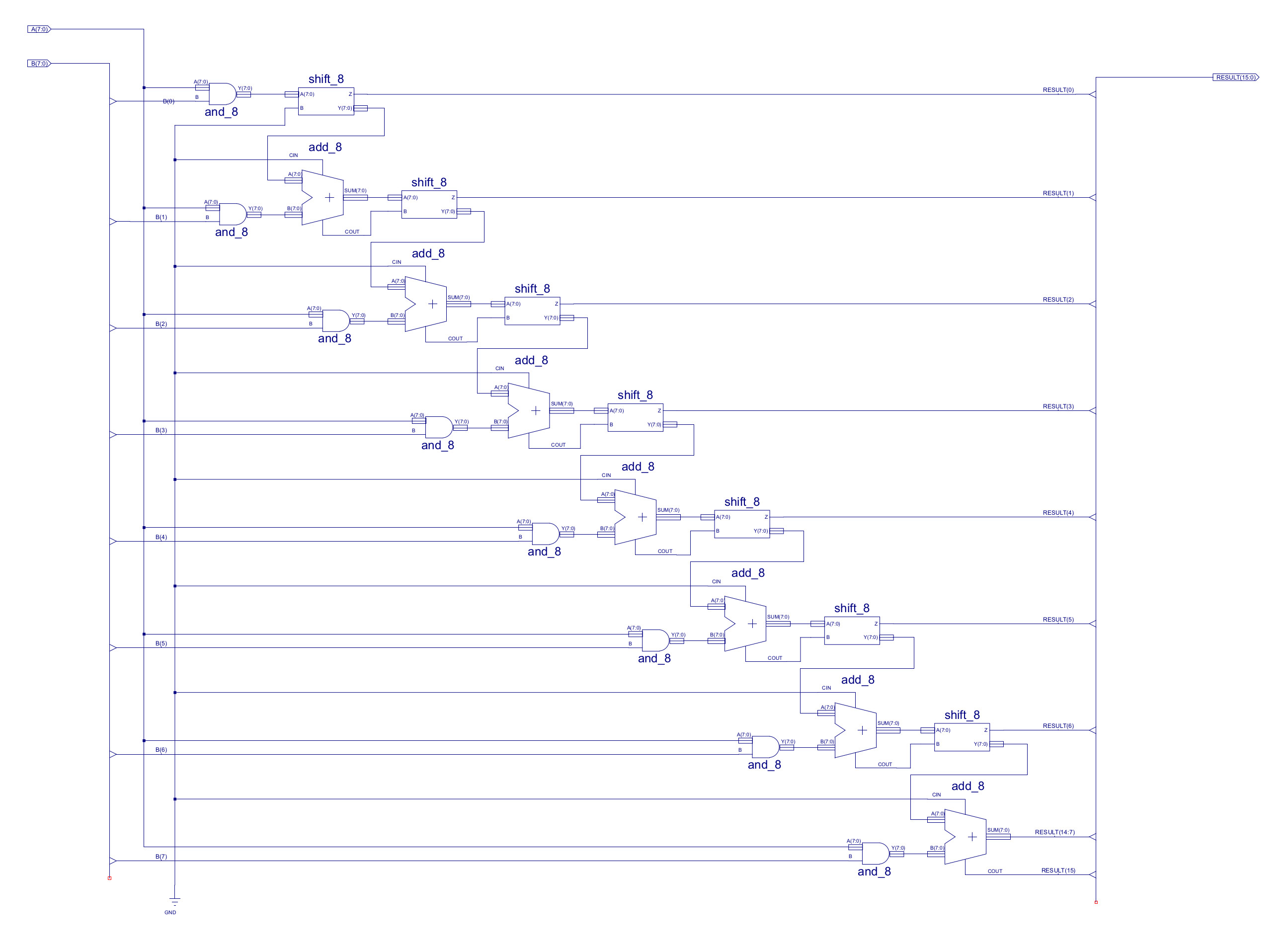
Figure 12 : multiplier schematic
One thing you can always guarantee when designing hardware is that the person that wants to use it will want to process bigger and smaller numbers. Then you hit the problems of overflows: number of bits used is not big enough to represent a value e.g. 256 in 8bits, or underflows: when the result produced is tooo small to be represented using the binary encoding used e.g. 0.1 in 8bits. This typically means moving to a floating, or fixed point representation. As i want to keep things simple i.e. keep the hardware simple, we are going to use a fixed point representation. This does add some issues, but for the moment lets consider underflows, as shown in figure 13.
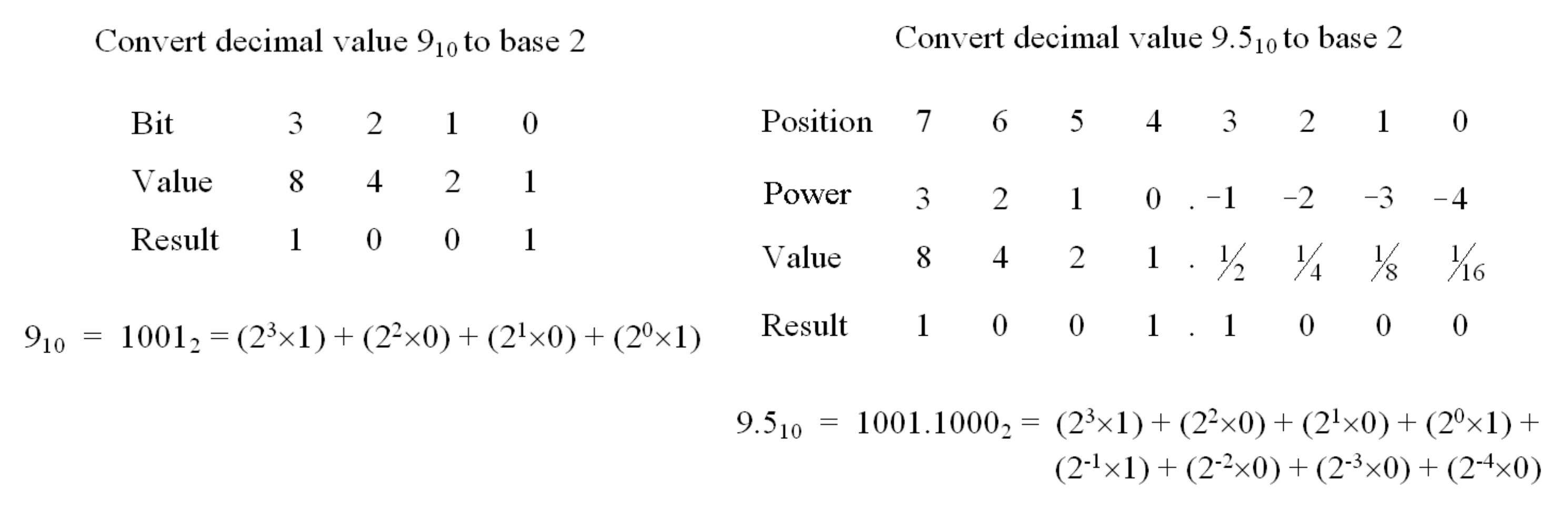
Figure 13 : fixed point
If we want to present the value 9.5, in the current hardware this will be truncated to 9 i.e. we have an underflow. Real numbers can be represented using a fixed point representation i.e. by inserting an imaginary decimal point into the binary number. Therefore, digits to the left of the decimal point represent the positive powers of two (1,2,4,8…) and those to the right represent the negative powers of two (1/2, 1/4, 1/8…), as shown in figure 13. Note, this decimal point is just an imaginary concept used by the programmer i.e. there is no hardware used to represent this decimal point, therefore, the existing adder and other functional blocks can be used, as the relative powers of 2 between each column remains the same. Consider the fixed point value below, it has m integer bits and n fractional bits, commonly referred to as a Qm.n format i.e. this value uses a Q8.8 number format.
9.5 = 00001001.10000000

Unsigned Q8.8 Min=0, Max=255.99609375
Signed Q8.8 Min=−128, Max=127.99609375

Resolution = 2^-8 = 0.00390625
For the simpleCPU this fits nicely into our data registers and memory i.e. 16bit values. We improve the resolution, but at the cost of range, sooo we need to process larger values e.g. 32bit values allowing a Q16.16 or a Q24.8 representation, or process even larger values, 64bit, 128bit etc. However, we do not want to have to create a 128bit adder etc, sooo we need instruction that will allow the hardware to break these task down into 16bit chunks i.e. the size of our registers and ADDER. Therefore, we have the instruction below:
INSTR   IR15 IR14 IR13 IR12 IR11 IR10 IR09 IR08 IR07 IR06 IR05 IR04 IR03 IR02 IR01 IR00
ADD     0    0    0    1    RD   RD   0    0    K    K    K    K    K    K    K    K
ADDC    0    0    0    1    RD   RD   1    0    K    K    K    K    K    K    K    K
SUB     0    0    1    0    RD   RD   0    0    K    K    K    K    K    K    K    K
SUBC    0    0    1    0    RD   RD   0    1    K    K    K    K    K    K    K    K

ADDM    0    1    1    0    A    A    A    A    A    A    A    A    A    A    A    A
ADDMC   1    1    0    0    A    A    A    A    A    A    A    A    A    A    A    A
SUBM    0    1    1    1    A    A    A    A    A    A    A    A    A    A    A    A
SUBMC   1    1    0    1    A    A    A    A    A    A    A    A    A    A    A    A

ADD     1    1    1    1    RD   RD   RS   RS   X    X    X    0    0    1    1    0
ADDC    1    1    1    1    RD   RD   RS   RS   X    X    X    0    1    1    1    1
SUB     1    1    1    1    RD   RD   RS   RS   X    X    X    0    0    1    1    1
SUBC    1    1    1    1    RD   RD   RS   RS   X    X    X    1    0    0    0    0


Example            :    add RB 2
Addressing mode    :    immediate
Opcode             :    0001 00
RTL                :    RX <- RX + ( (K7)8 || KK )
Flags set          :    Z,C,O,P,N
Description        :    signed addition

Example            :    addc RB 2
Addressing mode    :    immediate
Opcode             :    0001 10
RTL                :    RX <- RX + ( (K7)8 || KK ) + carry flag
Flags set          :    Z,C,O,P,N
Description        :    signed addition + carry flag

Example            :    sub RB 2
Addressing mode    :    immediate
Opcode             :    0010 00
RTL                :    RX <- RX - ( (K7)8 || KK )
Flags set          :    Z,C,O,P,N
Description        :    signed subtraction

Example            :    subc RB 2
Addressing mode    :    immediate
Opcode             :    0010 10
RTL                :    RX <- RX - ( (K7)8 || KK ) - carry flag
Flags set          :    Z,C,O,P,N
Description        :    signed subtraction + carry flag

Example            :    addm RA 123
Addressing mode    :    absolute
Opcode             :    0110
RTL                :    RA <- RA + M[123]
Flags set          :    Z,C,O,P,N
Description        :    signed addition

Example            :    addmc RA 124
Addressing mode    :    absolute
Opcode             :    1100
RTL                :    RA <- RA + M[124] + carry flag
Flags set          :    Z,C,O,P,N
Description        :    signed addition + carry flag

Example            :    subm RA 125
Addressing mode    :    absolute
Opcode             :    0111
RTL                :    RA <- RA - M[125]
Flags set          :    Z,C,O,P,N
Description        :    signed subtraction

Example            :    submc RA 126
Addressing mode    :    absolute
Opcode             :    1101
RTL                :    RA <- RA - M[126] - carry flag
Flags set          :    Z,C,O,P,N
Description        :    signed subtraction - carry flag

Example            :    add RA RB
Addressing mode    :    register
Opcode             :    1111 00110
RTL                :    RX <- RX + RY
Flags set          :    Z,C,O,P,N
Description        :    signed addition

Example            :    addc RB RC
Addressing mode    :    register
Opcode             :    1111 01111
RTL                :    RX <- RX + RY + carry flag
Flags set          :    Z,C,O,P,N
Description        :    signed addition + carry flag

Example            :    sub RC RD
Addressing mode    :    register
Opcode             :    1111 00111
RTL                :    RX <- RX - RY
Flags set          :    Z,C,O,P,N
Description        :    signed subtraction

Example            :    subc RD RA
Addressing mode    :    register
Opcode             :    1111 10000
RTL                :    RX <- RX - RY - carry flag
Flags set          :    Z,C,O,P,N
Description        :    signed subtraction - carry flag
Consider the example shown in figure 14. Confess this is a SimpleCPUv1a example, i didn't want to have redraw the figures, but it does still make the point :). Sooo, in this example the value 1000 decimal is split into two 7bit chunks, stored in two memory locations. Therefore, if we wanted to perform the calculation 1000 + 1000 i.e. add together the four chucks stored in four memory locations, we can break this down into two steps:
STEP1 : use ADDM instruction to add low 7bit memory locations together,
        store any carry produced in carry flag
STEP2 : use ADDMC instruction to add high 7bit memory locations together + any carry from STEP1,
        store any carry produced in carry flag
Sooo, when we perform a ADDM i.e. add the low 7bits, the EN=0, setting CIN to 0. When we perform a ADDMC i.e. add the high 7bits, the EN=1, setting CIN to the previously generated carry flag (C). Key thing to spot is that we are not testing to see if a carry was generated by the low 7bit addition we simple add it to the high 7bits i.e. if no carry was produced then C=0 so we add 0, if there was a carry produced C=1 so we add 1.
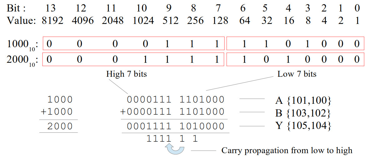
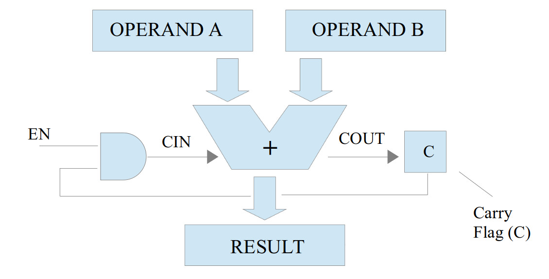
Figure 14 : carry propagation between ADD instructions
Using this technique we can add (or subtract) any size of number stored in external memory, the first add will be an ADDM, then every additional "chunk" will be added together using an ADDMC instruction, so to add together two 32bit numbers:
# Add together two 32bit values Y=A+B

start:
  load RA A_low     # read A low 16bits into RA
  addm RA B_low     # add to RA B low 16bits
  store RA Y_low    # save result to Y low 16bits
  load RA A_high    # read A high 16bits into RA
  addmc RA B_high   # add to RA B high 16bits
  store RA Y_high   # save result to Y high 16bits

trap:
  jump trap

A_low:
  .data 0           # variable A low 16bits
A_high:
  .data 0           # variable A high 16bits

B_low:
  .data 0           # variable B low 16bits
B_high:
  .data 0           # variable B high 16bits

Y_low:
  .data 0           # variable Y low 16bits
Y_high:
  .data 0           # variable Y high 16bits
We can now use these instruction to process fixed point values e.g. Q16:16 bit values, stored across two memory locations. Note, remember the processor has no knowledge of the fixed point, or values bigger than 16bits.
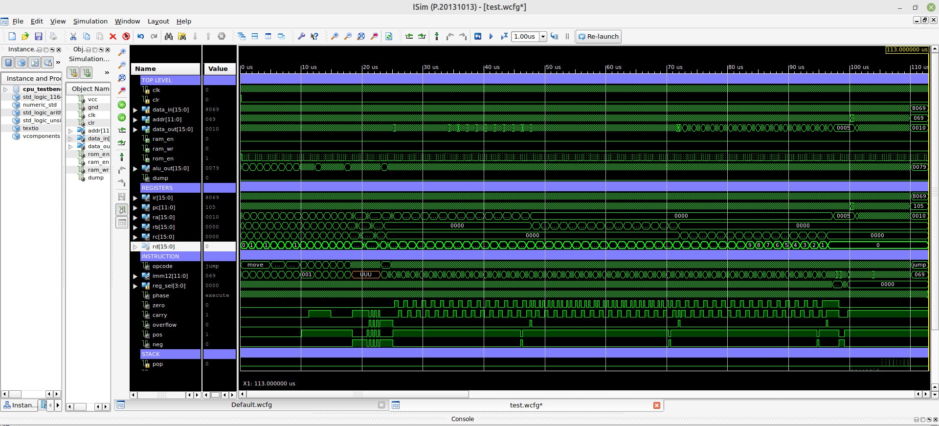
Figure 15 : simulation waveform
As always it easy to design new hardware, the hard part is getting it to work :). To test out these new instructions i wrote this test code. At this time it seems to be working correctly, fingers crossed, but i have not tested all instruction yet :).
###############################
# SIMPLECPU V1d2 TEST PROGRAM #
###############################

start:
  move RA 0x01        # RA = 0x0001
  move RB 0x01        # RB = 0x0001
  move RC 0x01        # RC = 0x0001
  move RD 0x01        # RD = 0x0001

  move RA 0x80        # RA = 0xFF80
  move RB 0x80        # RB = 0xFF80
  move RC 0x80        # RC = 0xFF80
  move RD 0x80        # RD = 0xFF80

  moveh RA 0x01       # RA = 0x0100
  moveh RB 0x01       # RB = 0x0100
  moveh RC 0x01       # RC = 0x0100
  moveh RD 0x01       # RD = 0x0100

  moveh RA 0x80       # RA = 0x8000
  moveh RB 0x80       # RB = 0x8000
  moveh RC 0x80       # RC = 0x8000
  moveh RD 0x80       # RD = 0x8000

  moveu RA 0x01       # RA = 0x0001
  moveu RB 0x01       # RB = 0x0001
  moveu RC 0x01       # RC = 0x0001
  moveu RD 0x01       # RD = 0x0001

  moveu RA 0x80       # RA = 0x0080
  moveu RB 0x80       # RB = 0x0080
  moveu RC 0x80       # RC = 0x0080
  moveu RD 0x80       # RD = 0x0080

  add RA 0x01         # RA = 0x0081
  add RB 0x01         # RB = 0x0081
  add RC 0x01         # RC = 0x0081
  add RD 0x01         # RD = 0x0081

  sub RA 0x01         # RA = 0x0080
  sub RB 0x01         # RB = 0x0080
  sub RC 0x01         # RC = 0x0080
  sub RD 0x01         # RD = 0x0080

  move RA 0xFF        # RA = 0xFFFF
  move RB 0xFF        # RB = 0xFFFF
  move RC 0xFF        # RC = 0xFFFF
  move RD 0xFF        # RD = 0xFFFF

  and RA 0x55         # RA = 0x0055
  and RB 0x55         # RB = 0x0055
  and RC 0x55         # RC = 0x0055
  and RD 0x55         # RD = 0x0055

  or RA 0xAA          # RA = 0x00FF
  or RB 0xAA          # RB = 0x00FF
  or RC 0xAA          # RC = 0x00FF
  or RD 0xAA          # RD = 0x00FF

  xor RA 0xCC         # RA = 0x0033
  xor RB 0xCC         # RB = 0x0033
  xor RC 0xCC         # RC = 0x0033
  xor RD 0xCC         # RD = 0x0033

  addm RA one         # RA = 0x0034
  subm RA one         # RA = 0x0033

                      # store RA to memory data 0-9
  store RA data0      # RA = 0x0033
  addm RA one         # RA = 0x0034
  store RA data1
  addm RA one         # RA = 0x0035
  store RA data2
  addm RA one         # RA = 0x0036
  store RA data3
  addm RA one         # RA = 0x0037
  store RA data4
  addm RA one         # RA = 0x0038
  store RA data5
  addm RA one         # RA = 0x0039
  store RA data6
  addm RA one         # RA = 0x003A
  store RA data7
  addm RA one         # RA = 0x003B
  store RA data8
  addm RA one         # RA = 0x003C
  store RA data9
  addm RA one         # RA = 0x003D

                      # load memory data 0-9
  load RA data0       # RA = 0x0033
  load RA data1       # RA = 0x0034
  load RA data2       # RA = 0x0035
  load RA data3       # RA = 0x0036
  load RA data4       # RA = 0x0037
  load RA data5       # RA = 0x0038
  load RA data6       # RA = 0x0039
  load RA data7       # RA = 0x003A
  load RA data8       # RA = 0x003B
  load RA data9       # RA = 0x003C

  move RA 0xFF        # RA = 0xFFFF
  move RB 0xFF        # RB = 0xFFFF
  move RC 0xFF        # RC = 0xFFFF
  move RD 0xFF        # RD = 0xFFFF

  asl RA              # RA = 0xFFFE 1111 1111 1111 1110
  shl RA              # RA = 0xFFFD 1111 1111 1111 1101
  asl RB              # RB = 0xFFFE
  shl RB              # RB = 0xFFFD
  asl RC              # RC = 0xFFFE
  shl RC              # RC = 0xFFFD
  asl RD              # RD = 0xFFFE
  shl RD              # RD = 0xFFFD

  asr RA              # RA = 0x7FFE 0111 1111 1111 1110
  shr RA              # RA = 0xBFFF 1011 1111 1111 1111
  asr RB              # RB = 0x7FFE
  shr RB              # RB = 0xBFFF
  asr RC              # RC = 0x7FFF
  shr RC              # RC = 0xBFFF
  asr RD              # RD = 0x7FFF
  shr RD              # RD = 0xBFFF

  move RA 0x00        # RA = 0x0000
  move RB 0x00        # RB = 0x0000
  move RC 0x00        # RC = 0x0000
  move RD 0x00        # RD = 0x0000

  move RD 48          # walk a 1 through RA, RB and RC
  move RA 1           # RD is loop counter
loop:
  asl RA
  shl RB
  shl RC
  sub RD 1
  jumpnz loop

  move RB 0x00        # compare RA to 5
  move RA 5           # RB 0=OK, 1=ERROR
  cmp RA 5
  jumpz cmp_eq        # is RA = 5

  move RB 0xFF

cmp_eq:
  cmp RA 10           # is RA = 10
  jumpz cmp_neq
  jump next

cmp_neq:
  move RB 0xFF

next:
  test RA 1           # is RA(0) 1?
  jumpnz test_eq

  move RB 0xFF

test_eq:
  test RA 2           # is RA(1) 1?
  jumpz test_neq
  jump next1

test_neq:
  move RB 0xFF

next1:
  call subA           # test nested subroutines
  move RA 16          # call depth 8, if working correctly the value
                      # 1 to 15 should be stored in register RA
trap:
  jump trap           # finish

subA:
  move RA 1           # subroutine A
  call subB
  move RA 15
  ret

subB:
  move RA 2           # subroutine B
  call subC
  move RA 14
  ret

subC:
  move RA 3           # subroutine C
  call subD
  move RA 13
  ret

subD:
  move RA 4           # subroutine D
  call subE
  move RA 12
  ret

subE:
  move RA 5           # subroutine E
  call subF
  move RA 11
  ret

subF:
  move RA 6           # subroutine F
  call subG
  move RA 10
  ret

subG:
  move RA 7           # subroutine G
  call subH
  move RA 9
  ret

subH:
  move RA 8           # subroutine H
  ret

one:
  .data 1

data0:
  .data 0
data1:
  .data 0
data2:
  .data 0
data3:
  .data 0
data4:
  .data 0
data5:
  .data 0
data6:
  .data 0
data7:
  .data 0
data8:
  .data 0
data9:
  .data 0
WORK IN PROGRESS

This work is licensed under a Creative Commons Attribution-NonCommercial-NoDerivatives 4.0 International License.
Contact email: mike@simplecpudesign.com