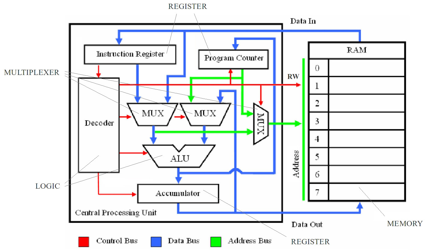
Figure 1 : Simple CPU
Modern CPU's are complex beasts, highly optimised and tricky to understand. This makes it very difficult to see why one was constructed in the way it was. Part of the problem is the requirement for backwards compatibility i.e. a new processor has to be able to run code from the previous generations. This incremental development can result in a very confusing instruction-set and a 'cluttered' hardware architecture. Also, when you do start to dig down into the literature a lot of things are not always fully disclosed i.e. to protect those industrial secrets. However, at their hearts all processors are simple machines and in some respects have not changed that much since the 1940s i.e. they still use instructions and perform a Fetch-Decode-Execute cycle. Therefore, to prove that processors are actually very simple to build and understand i developed a simple 8bit CPU architecture that can be implemented in an FPGA. To be honest it wasn't really designed, it evolved, therefore, the hardware could be optimised quite a bit. However, the aim was to break the processor down into its fundamental building blocks i.e. Boolean logic gates. Then combining these to form more complex components e.g. adders, multiplexers, flip-flop, counters etc, which are at the heart of any computer. The basic block diagram of this computer is shown in figure 1, a very simple machine, made from registers, multiplexers and an adder. The operation of this machine and its components will be explained from the bottom up, logic gates to "Hello World", implemented in a Spartan 3 FPGA, its hardware defined in schematics. The source files for each version of this processor can be downloaded (links in each section) and simulated using the Xilinx ISE 14.7 ISim tool.
Back to Basics - simpleCPU_v1
Testing: "Hello World"
Testing: fully tested :)
NOTE, some of the circuit diagrams are quite large, therefore, you may not be able to see signal / component names if viewed from this page. However, if you click on an image you will get a high resolution image, but some are quite large, so may take a while to load. PDFs are also available for some images.
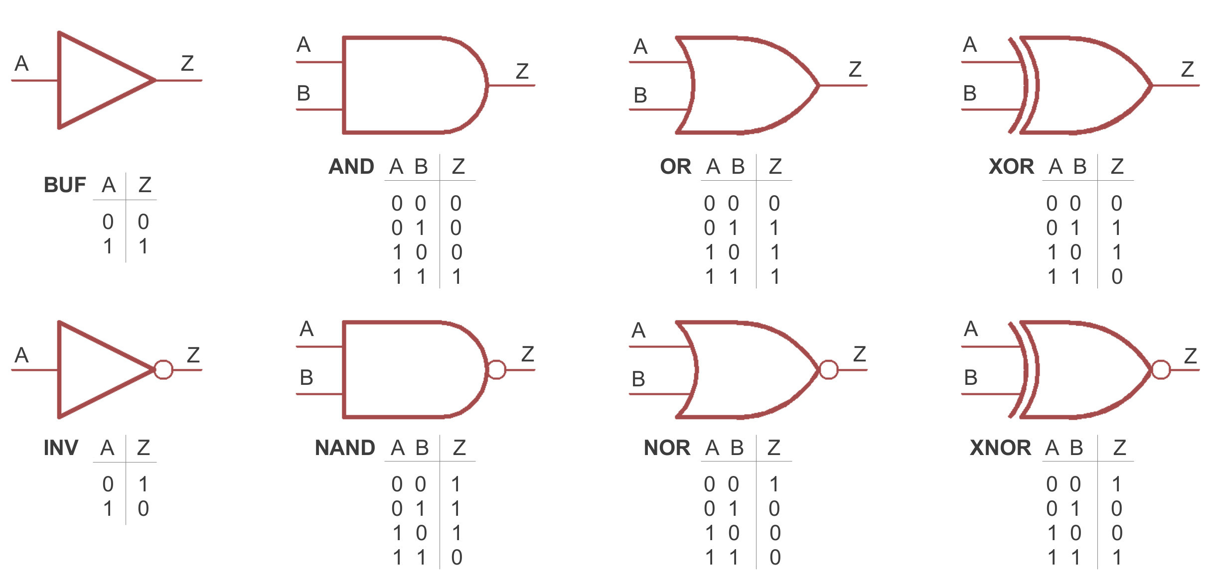

Figure 2 : Logic gates, symbols (top), waveform (bottom)
At its lowest level every operation in the computer is performed by logic gates like those shown in figure 2, for more information on Boolean logic refer to: (Link) (Link). Using these basic building blocks we can construct the four fundamental components of any computer:
Referring back to figure 1 you can see that this processor has three multiplexers (MUX) controlling the data and address buses. Note, in its simplest form a bus is just a group of wires carrying a binary numbers (Link ). Multiplexers are switches allowing the processor to select information from multiple sources (buses) and route it to a single destination. To select which data source should be used a multiplexer has one or more control lines as shown in figure 3. This 2:1 MUX has two data inputs (A,B), one output (Z) and an input (SEL), selecting which one of the two data inputs should be connected to its output, as defined by its truth table shown in the bottom of figure 3. When SEL=0 input A is connected to the output Z. When SEL=1 input B is connected to the output Z.
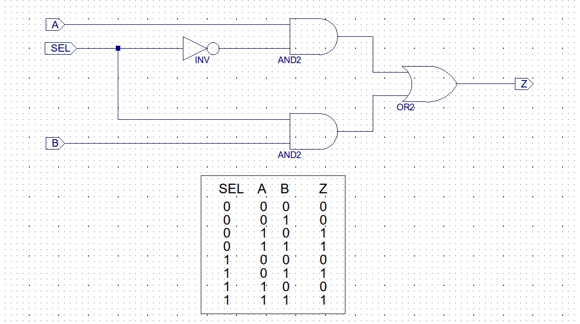
Figure 3 : 2:1 bit multiplexer, circuit diagram (top), truth table (bottom)
This multiplexer can select between two bits (binary digits), however, within the processor we need to select between 8 bit (byte) buses i.e. alternative data or address values. To achieved this the multiplexer is replicated eight times i.e. one per bit in the bus, as shown in figure 4. Note, each mux2_1_1 rectangle (symbol) contains the circuit shown in figure 3. To save space i have only shown the first three multiplexers, a full circuit diagram is available here: (Link ). The circuit symbol for this 8bit multiplexer is shown in figure 5, it's interface has three 8 bit buses (thick lines) and one signal (thin lines):
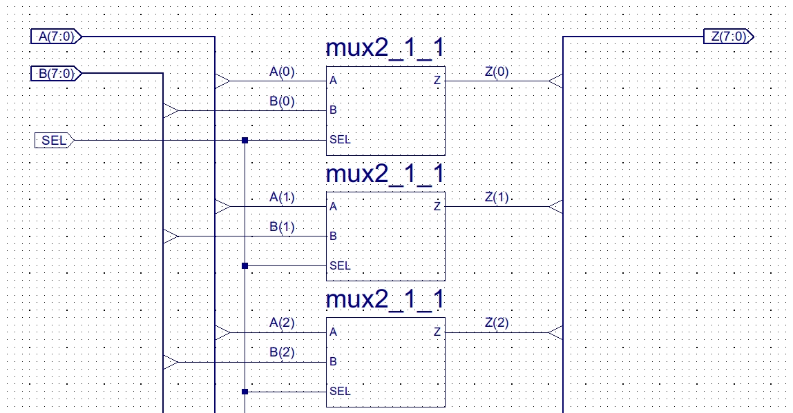
Figure 4 : 2:1 byte multiplexer circuit diagram (first three stages only)
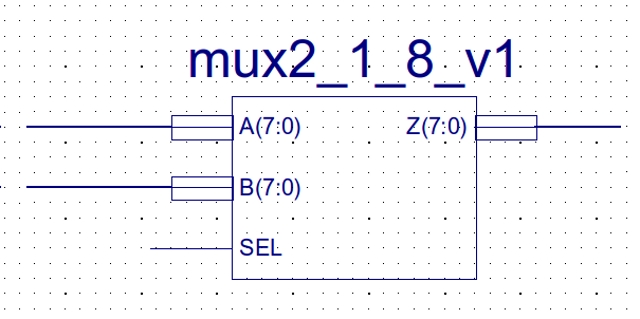

Figure 5 : 2:1 bye multiplexer, symbol (top), waveform (bottom)
Note, this approach of using hierarchical schematics is a good example of a fundamental design principle in computer science i.e. abstraction. Identifying key functionality, separating these out into distinct components, that can then be reused in the construction of other components or systems, simplifying schematic layout, construction and hides unnecessary details.
To state the obvious designing complex computing systems is a complex process, there is a large gap between user requirements and system realisation which is "difficult" (impossible) to perform in a single step. To simplify this design process we break the system down in to a number of functional blocks e.g. the top level block diagram shown in figure 1. We can then incrementally refine these components to a final implementation whilst ignoring irrelevant details.
In addition to 2:1 multiplexers shown in figure 1 the ALU also needs a 4:1 multiplexer (discussed later) i.e. a multiplexer that has four inputs and one output. This can be constructed from three 2:1 byte multiplexers, as shown in figure 6. Note, each mux2_1_8_v1 rectangle (symbol) contains the circuit shown in figure 3 i.e. 3 x 8 x 4 = 96 logic gates. The Xilinx schematics and symbols for these multiplexers can be downloaded here: (Link ). For more information on multiplexers refer to : (Link ).

Figure 6 : 4:1 byte multiplexer, circuit diagram and truth table
All number crunching is performed in the Arithmetic and Logic Unit (ALU), implementing the central processing units (CPU) main arithmetic functions. To implement an ADD function (one of the core instructions of any computer), there are a number of different hardware solutions, each having advantages and disadvantages. However, to avoid an in depth discussions of their relative merits i'm going to stick with the basic half adder, as shown in figure 7. For more information on adders refer to: (Link ) (Link ). This circuit adds together two bits A and B, producing a Sum and Carry. Working through the truth table you can see the addition process 0+0=0, 0+1=1, 1+0=1. As this is a binary (base 2) machine, the maximum value any digit can store is 1, therefore, when A=B=1 the Sum output can not represent the result of 2, so a Carry is generated. This Carry would then be added to next digit in the number.
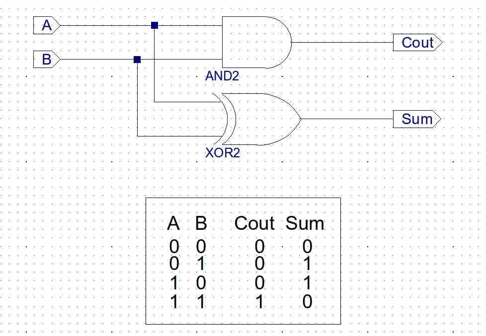
Figure 7 : Half adder, circuit diagram (top), truth table (bottom)
On its own a half adder is not that useful as we need to add together 8bit numbers, but it can be used as the building block for a full adder, as shown in figure 8. Note, each half_adder rectangle (symbol) contains the circuit shown in figure 7. This circuit can add together three bits: A,B and Cin. Another way to think about this circuit is that it counts the number of 1's:
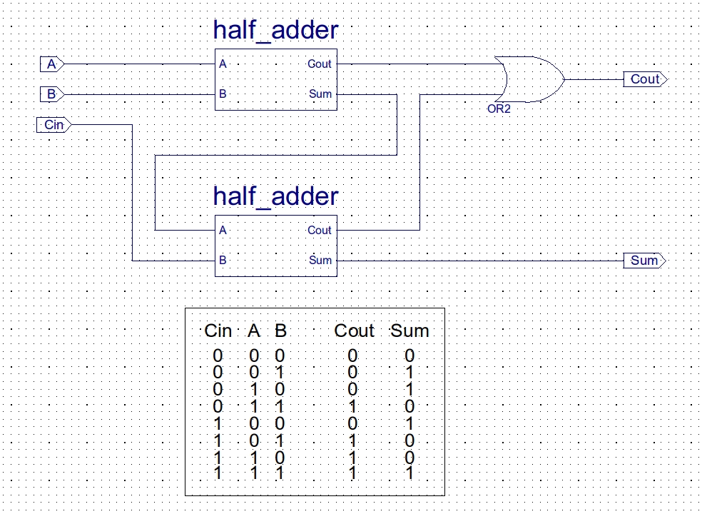

Figure 8 : Full adder, circuit diagram (top), truth table (middle), waveform (bottom)
Again at first glance the ability to add three bits together may not seem that useful, however, if we replicate this hardware eight times, connecting the Carry out (Cout) of the previous stage to the Carry in (Cin) of the next we can build a Ripple adder, as shown in figure 9. Note, again each rectangle (symbol) contains a sub-circuit, in this case full_adder shown in figure 8. To save space i have only shown the first three full adders, a full circuit diagram is available here: (Link ). An alternative way of considering this hardware is the pseudo code shown in figure 10. Each full adder is a modulus 2 adder, conceptually the addition process starts with the least significant digit (LSD) and 'ripples' through the hardware to the most significant digit (MSD) i.e. bits X0 and Y0 are added together to produce a Sum Z0 and a Carry C1, this Carry is then added to the next significant digits X1 and Y1 etc. This sequential behaviour does limit the hardware's performance. However, don't forget that the hardware associated with each digit's addition is all working in parallel e.g. best case performance: 987+12=999, no carries would be generated, the additions of 9+0, 8+1 and 7+2 would all be performed in parallel and complete in one unit of time. However, worst case performance: 999+1=1000, this would take four units of time owing to the carries having to ripple through the hardware from the LSD to the MSD. Note, its silly to say, but its important to remember that hardware is not software. When analysing hardware some elements may have a sequential behaviours, but ALL logic gates will be working in parallel (are active all the time).
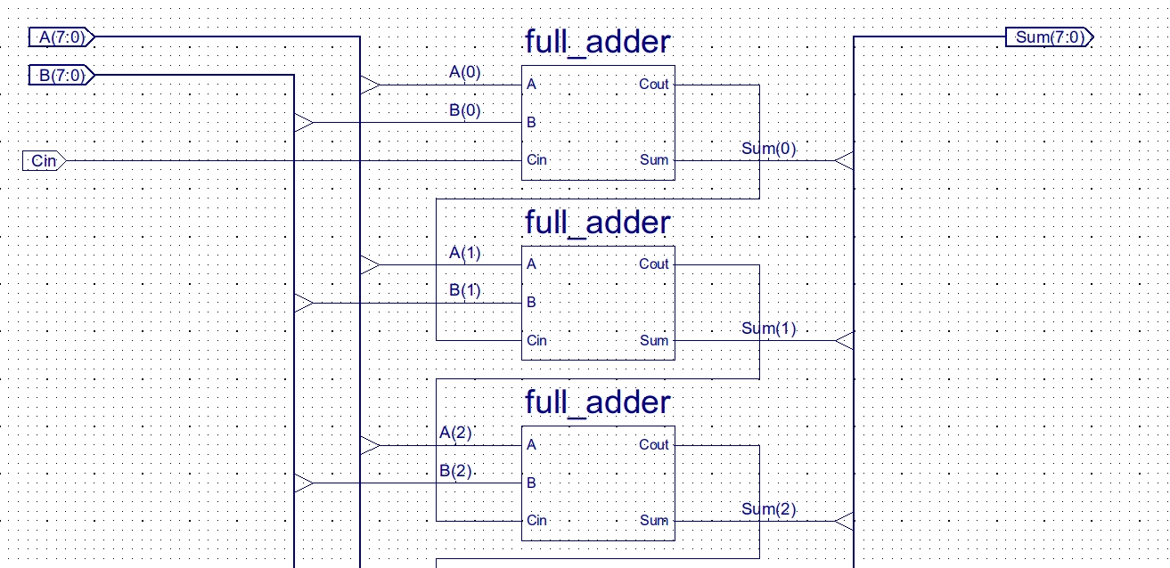
Figure 9 : Ripple adder circuit (first three stages only)
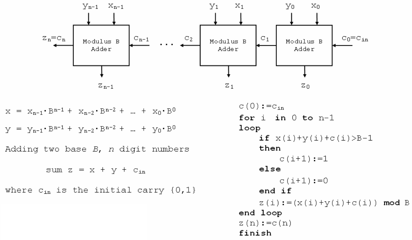
Figure 10 : Ripple adder architecture
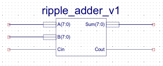
Figure 11 : Ripple adder symbol
The top level circuit symbol for the ripple adder is shown in figure 11 (containing the circuit shown in figure 9), this symbol's interface has three 8bit buses (thick lines) and two signals (thin lines):
The complete ALU circuit diagram is shown in figure 12. With a few small modifications the ripple adder can be used to implement a subtraction function. The subtraction hardware can be implemented using 2s complement (Link ) i.e. subtraction by the addition of negative numbers. To generate a negative number each bit is inverted and then 1 is added to the result, as shown in the example below.
    123     45 = 000101101   123 = 01111011      001111011
  -  45    inv = 111010010                     + 111010011
  -----     +1 = 111010011                     -----------
     78                                          001001110  = 78
  -----                                        -----------
                                                11111   1
To invert each bit an array of XOR logic gates are used, bitwise_inv_v1, as shown in figure 13. This circuit has an 8bit input bus (A), each bit is XORed with the signal EN. XORing a bit with 0, returns the same value. XORing a bit with 1, returns the inverse of that value. To add 1 the Carry-In (Cin) signal to the ripple adder is set to 1, incrementing the final result. In the ALU this is controlled using signals S2 and S3. The ADD and SUB functions can be simulated using the Xilinx ISim software tools, as shown in figure 14. In this waveform diagram the calculations 123+45 and 123-45 are performed. Remember, when you use a 2's complemented representation in a calculation the final Carry-out is ignored. The Xilinx schematics, symbols and VHDL testbench for this ALU can be downloaded here: (Link ).
  A B Z
  0 0 0       A XOR 0 = A
  0 1 1       A XOR 1 = NOT A
  1 0 1
  1 1 0
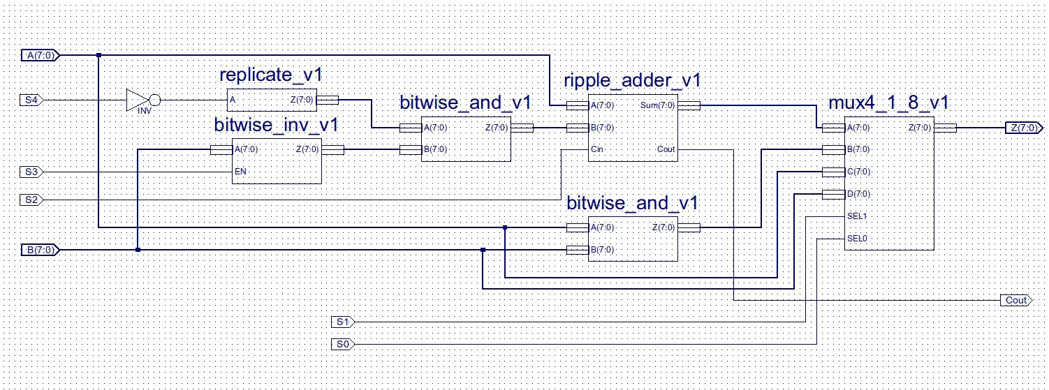
Figure 12 : ALU circuit diagram
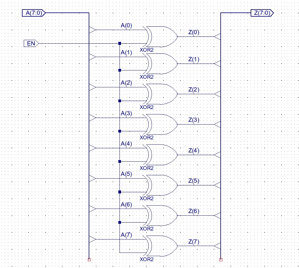
Figure 13 : Bitwise XOR
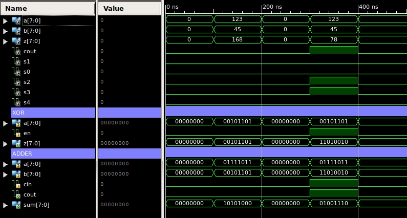
Figure 14 : ALU simulation, ADD and SUB
The Carry-in input can also be used to perform an increment function i.e. Z=A+0+1. This is quite a common requirement within a program e.g. incrementing a counter/variable, or the processor's program counter. To achieve this function the B input of the adder needs to be set to zero. To do this the replicate_v1 and bitwise_and_v1 circuits shown in figures 15 and 16 are used. The replicate_v1 component uses buffers (BUF) to drive the same signal onto each bit of its output bus Z. These signals are then ANDed with the data on the B input of the ALU. If they are ANDed with 1, the value on the B input of the adder is unaffected. If they are ANDed with 0, the value on the B input of the adder is set to zero. In the ALU this is controlled using signals S2 and S4. The INC function can be simulated using the Xilinx ISim software tools, as shown in figure 17. In this waveform diagram the calculations 123+1 and 45+1 are performed.
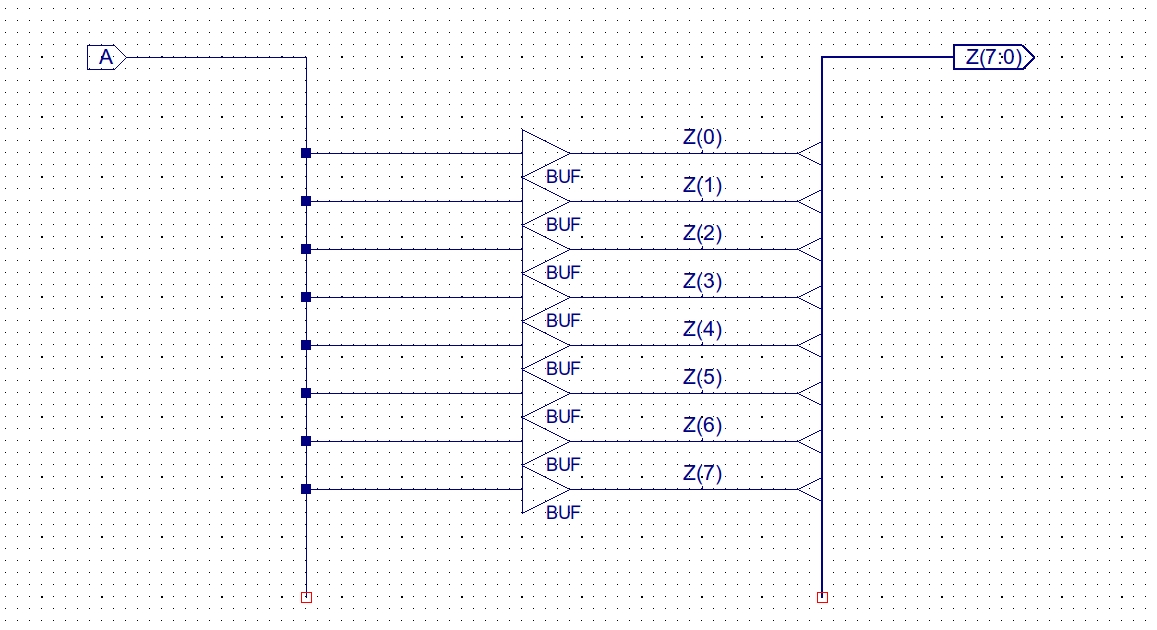
Figure 15 : replicate
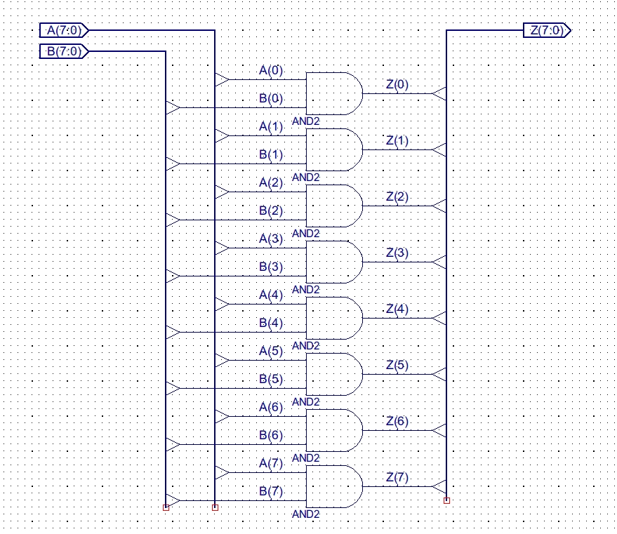
Figure 16 : Bitwise AND
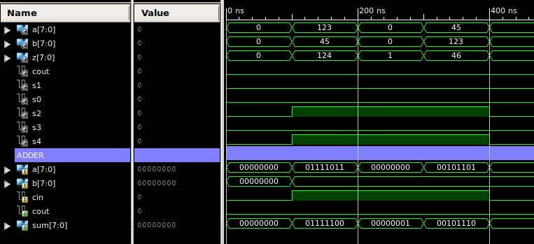
Figure 17 : ALU simulation, INC
The bitwise_and_v1 component is also used in the ALU to perform the bitwise AND function i.e. Z=A AND B, as shown in the example below. Note, at first glance this may not see that useful a function, but as we will see later its used a lot in programs to test the state of the internal registers etc.
  A B Z                           10101010
  0 0 0       A AND 0 = 0       & 11110000
  0 1 0       A AND 1 = A       ----------
  1 0 0                           10100000
  1 1 1                         ----------
To select the ALU's function the final 4:1 multiplexer is used, control lines S0 and S1 selecting either the adder's output, bitwise AND output, input A or Input B. The full set of control signals are shown below.
  S4 S3 S2 S1 S0  Z
  0  0  0  0  0   ADD (A+B)
  0  0  0  0  1   BITWISE AND (A&B)
  0  0  0  1  0   INPUT A
  0  0  0  1  1   INPUT B
  0  1  1  0  0   SUBTRACT (A-B)
  1  0  1  0  0   INCREMENT (A+1)
  1  0  0  0  0   INPUT A
  0  0  1  0  0   ADD (A+B)+1
  0  1  0  0  0   SUBTRACT (A-B)-1

Figure 18 : Arithmetic and Logic Unit (ALU) symbol
Computer's execute instructions using the Fetch-Decode-Execute cycle (Link), therefore, the processor must remember what phase it is in so that it can progress to the next. This temporary memory is implemented using flip-flops, each storing 1 bit of data, as defined by the state table shown in figure 19. A flip-flop has an input pin D and an output pin Q, the value on D is written to Q when there is a change from a logic 0 to a logic 1 on the CLK pin. Another way to think about the CLK pin is that it is the write, or update control signal i.e. the CLK line is pulsed to store a value. Owing to electronic reasons which i will quickly skip over all CLK lines must be connected to the same system clock i.e. a global square wave signal that determines the operating speed of the processor. This would mean that every flip-flop would update its output every clock cycle, which would not be very useful. Therefore, to control when different flip-flops update their outputs we use the clock enable input pin CE. If CE=0 the CLK pin is ignored. If CE=1 the CLK pin is used.
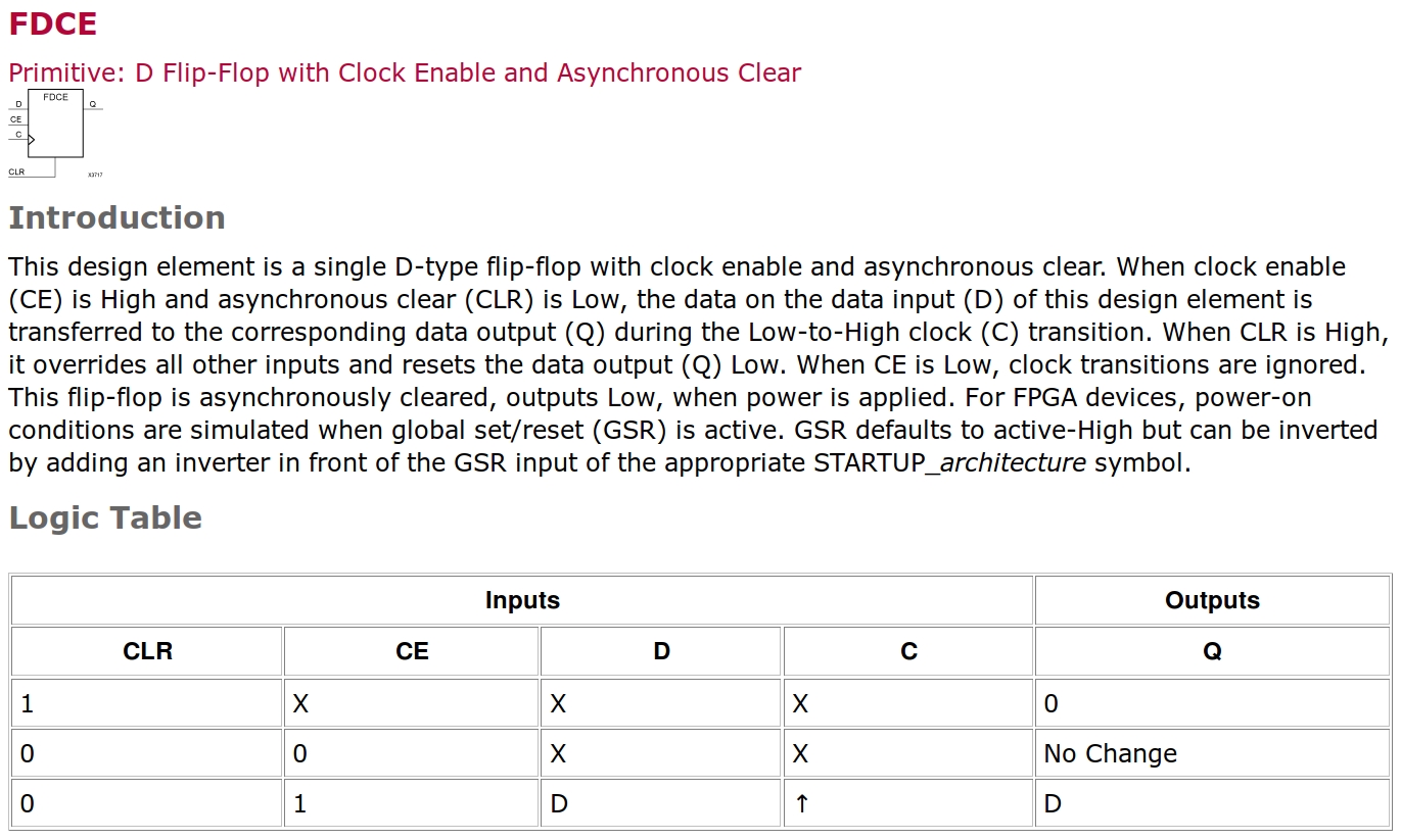
Figure 19 : D-type flip-flip
Within the processor temporary values are stored in registers, within a register each bit is stored in a flip-flop, as shown in figures 20, 21 and 22. To make larger registers multiple smaller registers are grouped together. Note, the rectangular components register_4 and register_8 contain the circuit diagrams shown in figure 20 and 21 respectively. The operation of the 8bit register can be simulated using the Xilinx ISim software tools, as shown in figure 23. In this waveform diagram the values 123 and 45 are stored in the register, using the CLK, CLR and CE lines to control when these values are updated. The Xilinx schematics, symbols and VHDL testbench for these registers can be downloaded here: (Link ).
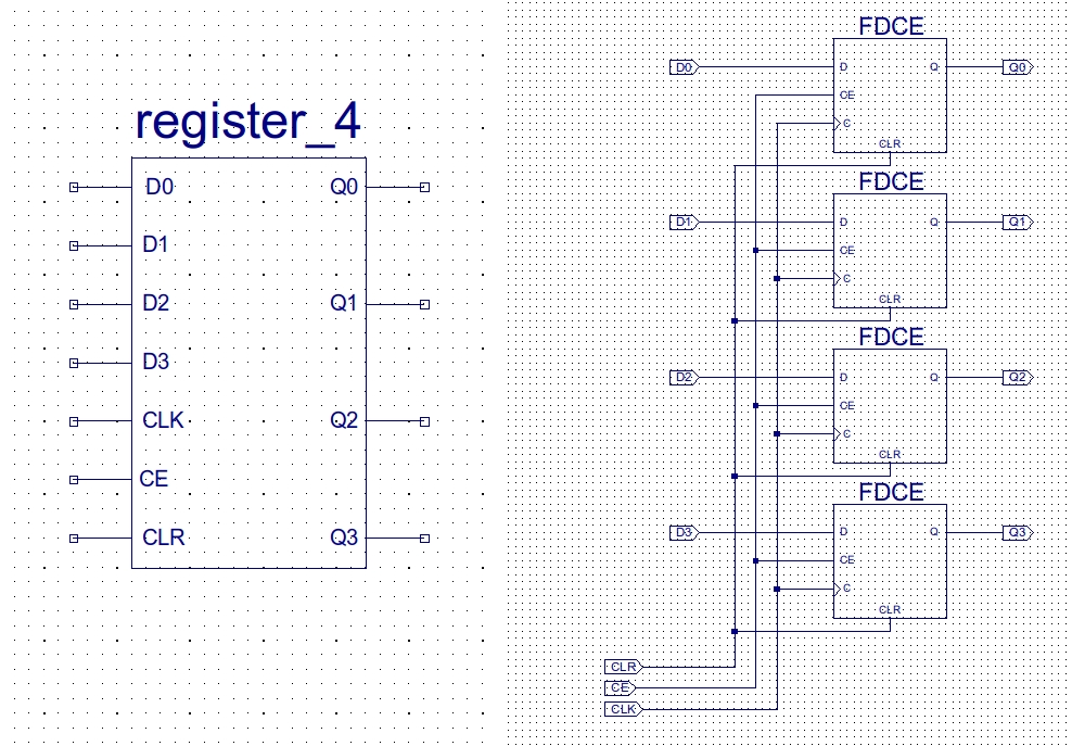
Figure 20 : Four bit register, symbol (left), circuit (right)

Figure 21 : Eight bit register, symbol (left), circuit (right)
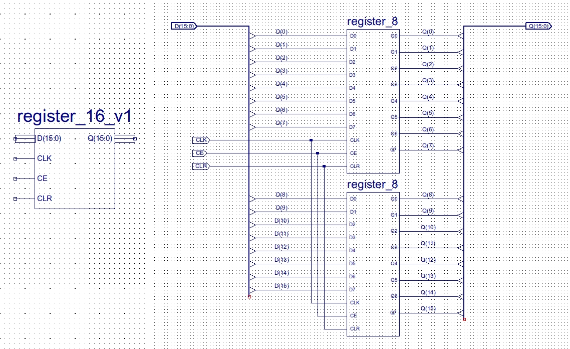
Figure 22 : Sixteen bit register, symbol (left), circuit (right)

Figure 23 : Eight bit register simulation
As shown in figure 1 this processor has three main registers:
Flip-flops are also used to generate the sequence of control signals needed to perform the functions defined by each instruction. These are contained within the decoder or control-logic block (figure 1), the circuit diagram symbol for this component is shown in figure 24. Inside this component are the instruction decoding logic and sequence generators needed to control the processor, as shown in figure 25. A high resolution diagram can be downloaded here: (Link ).
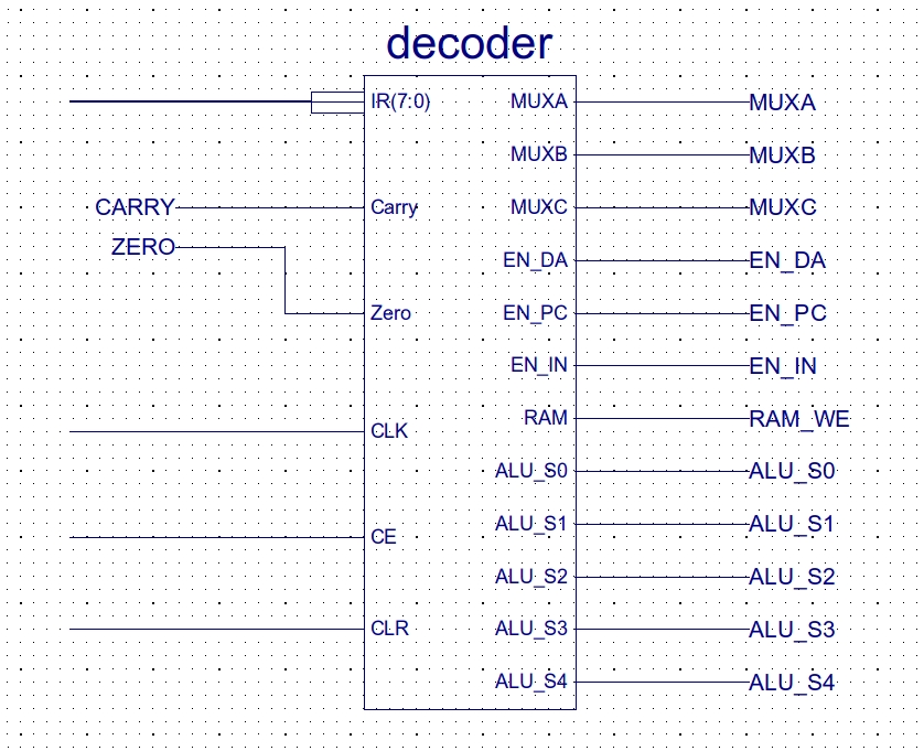
Figure 24 : Decoder symbol
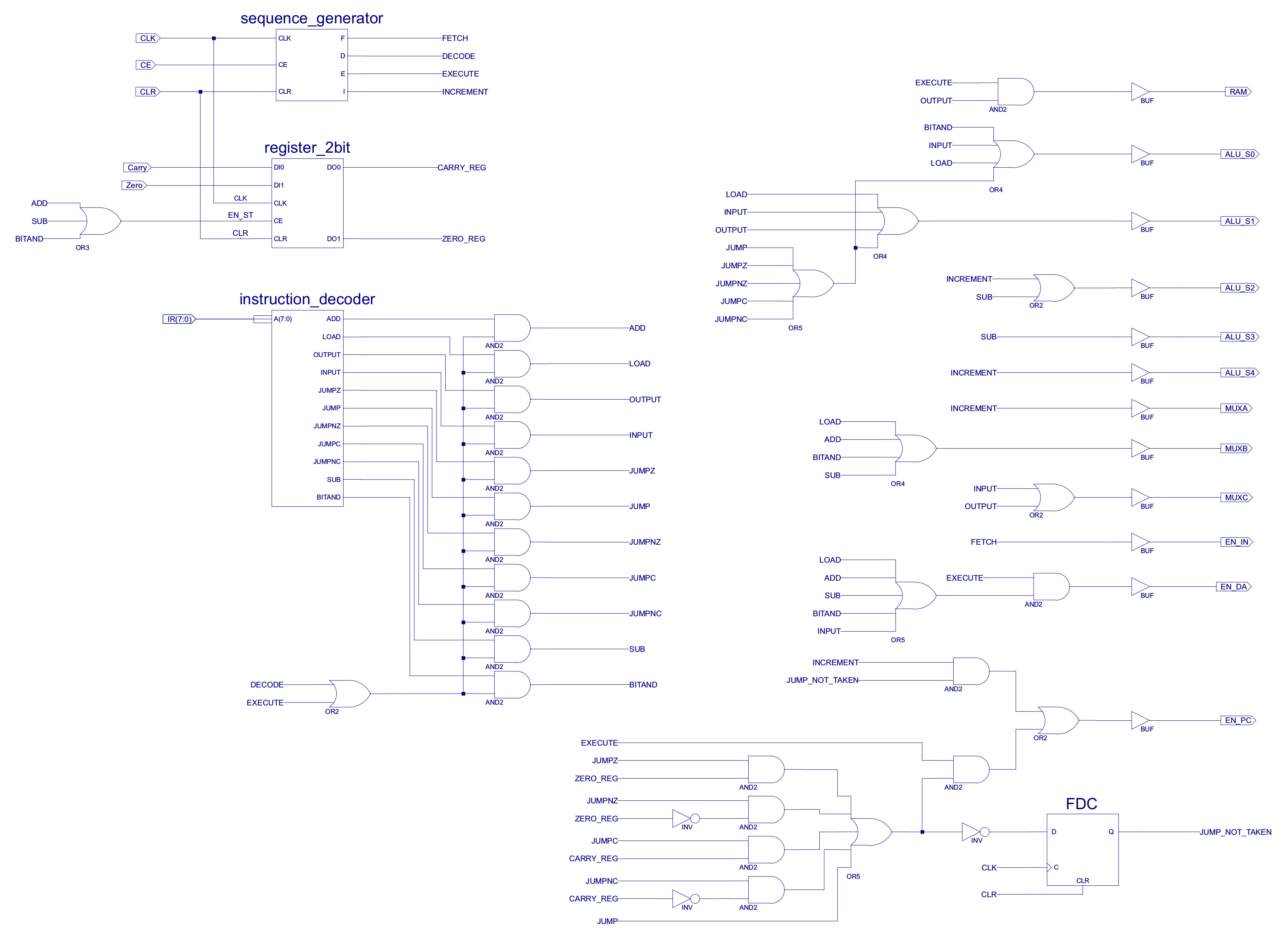
Figure 25 : Decoder circuit diagram
This processor has a slightly modified Fetch-Decode-Execute cycle. To save an adder (reduce hardware) i added an additional phase, it now has a Fetch-Decode-Execute-Increment cycle, the final phase incrementing the PC to the address of the next instruction (when needed).
Note, normally the PC update would be performed in the Fetch/Decode phase, i moved this into a separate phase to highlight these types of "housekeeping" operations are needed in the Fetch-Decode-Execute cycle i.e. you need to maintain the machinery within the processor that allows you to crunch instructions and data.
To identify which phase the processor is in a sequence generator is used, as shown in figures 26 and 27. This is a simple ring counter (Link), using a one-hot (Link) encoded value to indicate the processor's state, as shown in figure 28. Initially the value 1000 is loaded into the counter (fetch code), on each clock pulse the one-hot bit is then moved along the flip-flop chain, looping back to the start after four clock cycles. To determine the processor's state you simply identify which bit position is set to a logic 1. One-hot encoding i.e. when a number only ever has one bit set, is very easy to decode in hardware, but its sparse encoding means you need a lot of bits to represent larger values as not all bit states are used. A four bit one-hot value can represent 4 states, or the value 0 to 3, using a binary encoding you could represent the value 0 to 15, but you would need to decode all bits to determine its value, where as using one-hot you only need to look at one bit.
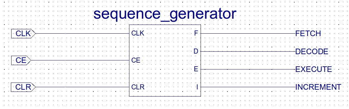
Figure 26 : Sequence generator symbol
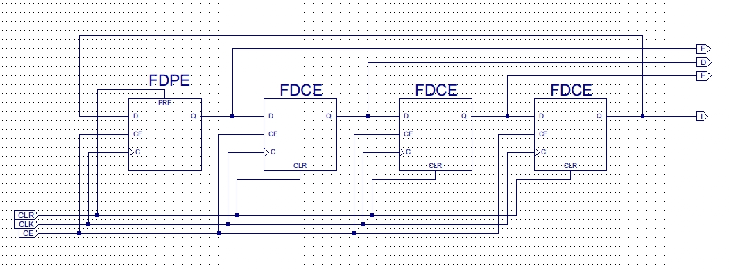
Figure 27 : Sequence generator

Figure 28 : Sequence generator simulation
During the Fetch phase the current instruction pointed to by the program counter (PC) is loaded into the instruction register (IR). Then in the decode phase the high byte of the 16bit, fixed length instruction is decoded by the instruction decoder shown in figure 29. A high resolution diagram can be downloaded here: (Link ). To simplify construction this processor has a very limited instruction set:
In this instruction syntax X=Not used, K=Constant, A=Instruction Address, P=Data Address. The complexity of an instruction is also defined by its addressing mode i.e. not just how much number crunching it does, but how it fetches its operands (data). Again, to simplify the required hardware these instructions are limited to simple addressing modes:
The register transfer level (RTL) description of each of these instructions is:
Note, in RTL syntax "<-" reads as "updated with", M[X] is memory, addressed at location X. For more information on addressing modes refer to: (Link).
The top 4 to 6 bits of each instruction defines the opcode: an unique binary pattern that allows the CPU to identify what function needs to be performed, where the data (operands) are and where any result produced should be stored. Note, the top nibble (4bit) of each instruction is unique to that instruction. For those of you who know your machine code you will recognise these instructions are based on the original PicoBlaze machine code (Link), another nice small 8 bit processor that i have used in Lectures. The instruction decoder shown in figure 29 converts the unique opcode into a one-hot value, these are then used during the Decode and Execute phases to control the processor's hardware. To ensure these signals are not active during the Fetch and Increment phases they are ANDed (zeroed) with the result of the logical OR of the Decode and Execute signals from the sequence generator, as shown in figure 30.
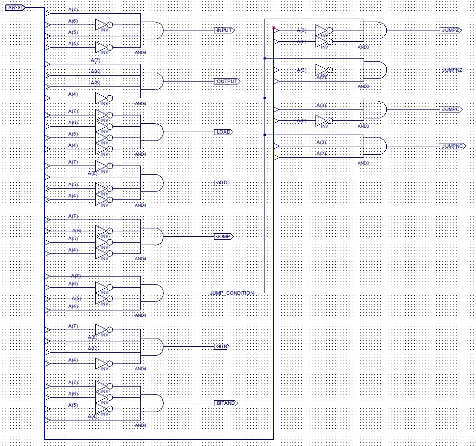
Figure 29 : Instruction decoder
Note, the AND gates in figure 29 decode the opcode field i.e. each zero in the opcode nibble is passed through a NOT gate, such that when a specific opcode is decoded only one AND gate will have all of its inputs driven to a logic one i.e. there will never be two AND gates producing a logic one at the same time (a one-hot encoded output).

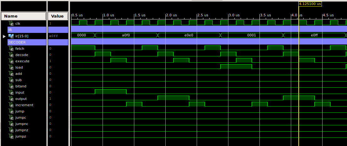
Figure 30 : Complete instruction decoder, circuit (top), waveform (bottom)
The processor supports unconditional and conditional JUMP instructions. The conditional JUMP instructions are based on the result of the last ALU operation i.e. the ZERO and CARRY bits for the ADD, SUB and AND instructions. These are stored in a 2bit register, as shown in figure 31. Note, the ZERO bit is generated by an 8bit NOR gate connected to the ALU's output bus i.e. a NOR only produce a 1 when all of its inputs are 0.
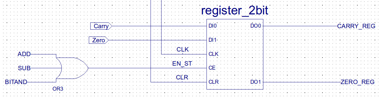
Figure 31 : Status register
The sequence_generator, instruction_decoder and status_register form the core elements of the processor's control unit (decoder block in figure 1). The signals from these units are used to generate the control signals for the system MUXs, ALU and REGs, as shown in figure 32. This table defines the state of each control signal, for each phase, to implement that instruction's function. This table also defines the control signals needed for the Fetch and Increment phases. The logic that drives these control signals (right hand side of figure 25) is derived from this table.

Figure 32 : Control signals
Most of this control logic is quite intuitive, you simply combine the one-hot output from the Decoder with the state bits from the Ring-counter to produce the logic 1's in each row of the table in figure 32. A slightly more complex bit is the Jump logic shown in figure 33. If the processor is in the Execute phase, the instruction decoder and status signals determine if the program counter (PC) should be updated i.e. should the jump address be loaded into the PC. If a JUMP instruction is taken, then the system does not need to increment the PC, as it already contains the address of the next instruction. Therefore, when the processor is in the Increment phase it checks to see if a jump has been taken, if it has been the PC is not enabled i.e. the result PC+1 is not stored in the program counter.
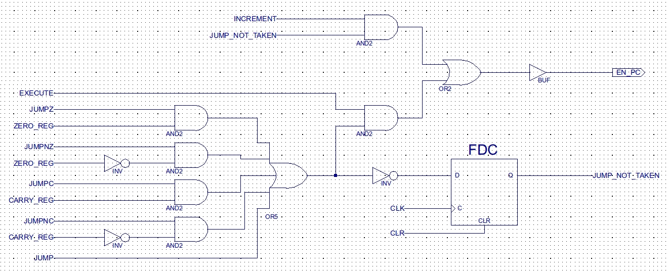
Figure 33 : Jump logic
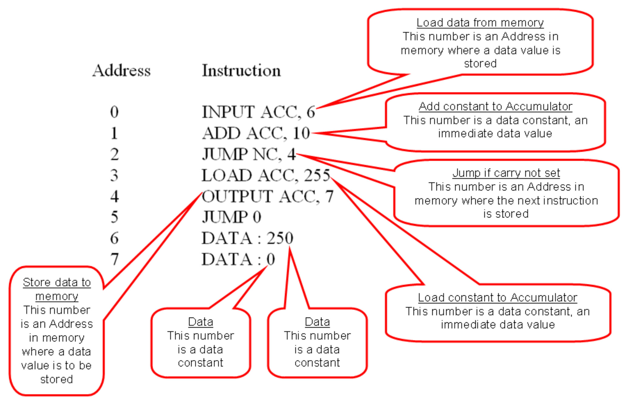
Figure 34 : test code
To illustrate the operation of this computer, consider the simple program in figure 34. This program adds two 8 bit unsigned numbers together and tests for an overflow. If an overflow occurs the result is saturated i.e. set to its maximum value (255). The step by step analysis of the execution of this program is shown in figures 35 to 37, adding the data values 250 and 10. This will cause an overflow to occur, resulting in the final result being saturated to 255. If however the data values used are 250 and 5, no overflow will occur as shown in figure 37. Note, in each phase the active address and data paths are highlighted dark BLUE.
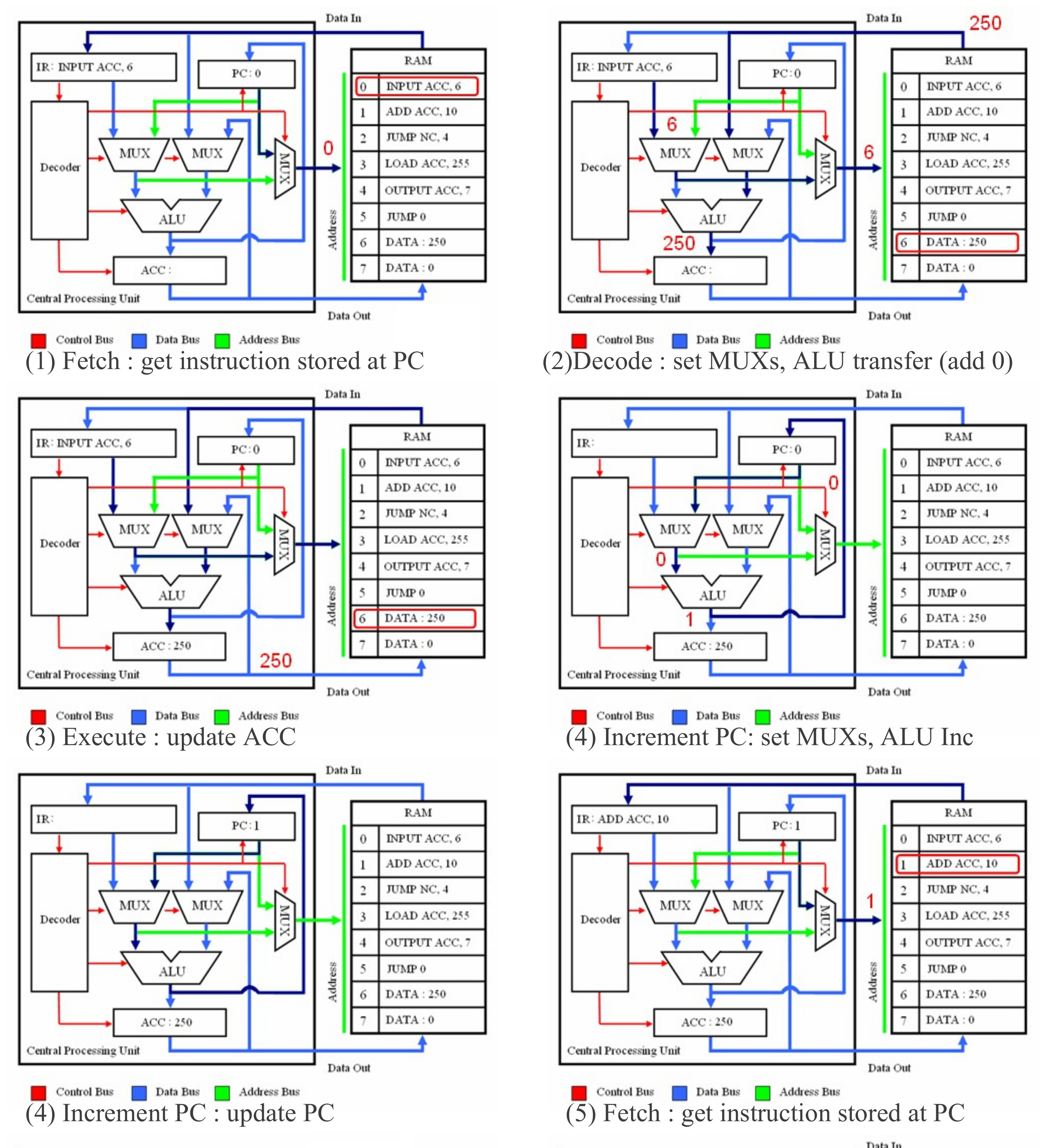
Figure 35 : steps 1 to 5
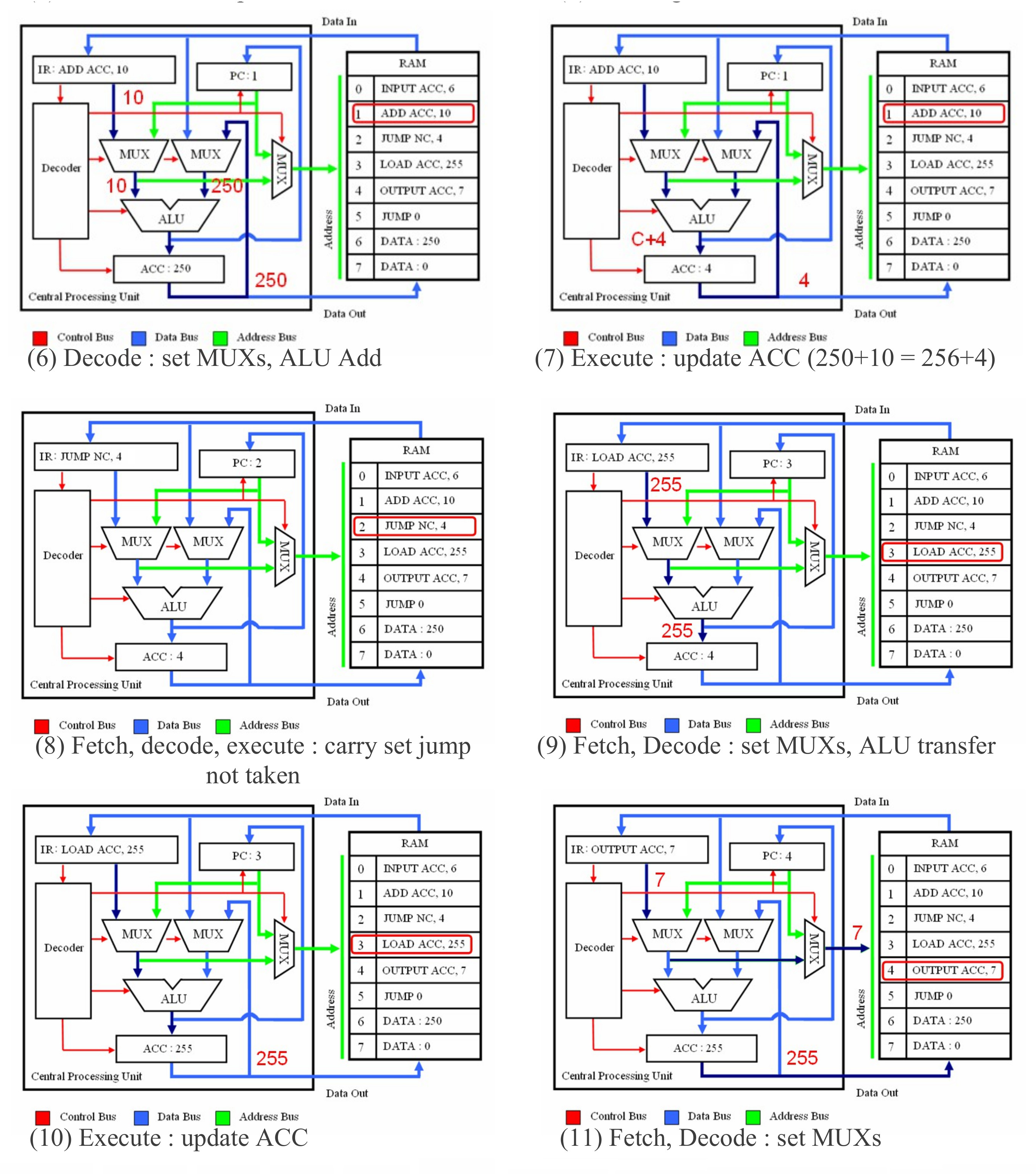
Figure 36 : steps 6 to 11
Note, a common misunderstanding is the differences between the LOAD and INPUT instructions. For this processor LOAD does not read memory. To read the contents of an external memory location we would use the INPUT instruction. The LOAD instruction is an internal operation copying the immediate value stored in the IR to the ACC, in the above example the constant 255. I agree is this confusing if you have used other processors, but for this processor i decided to follow PicoBlaze syntax :)
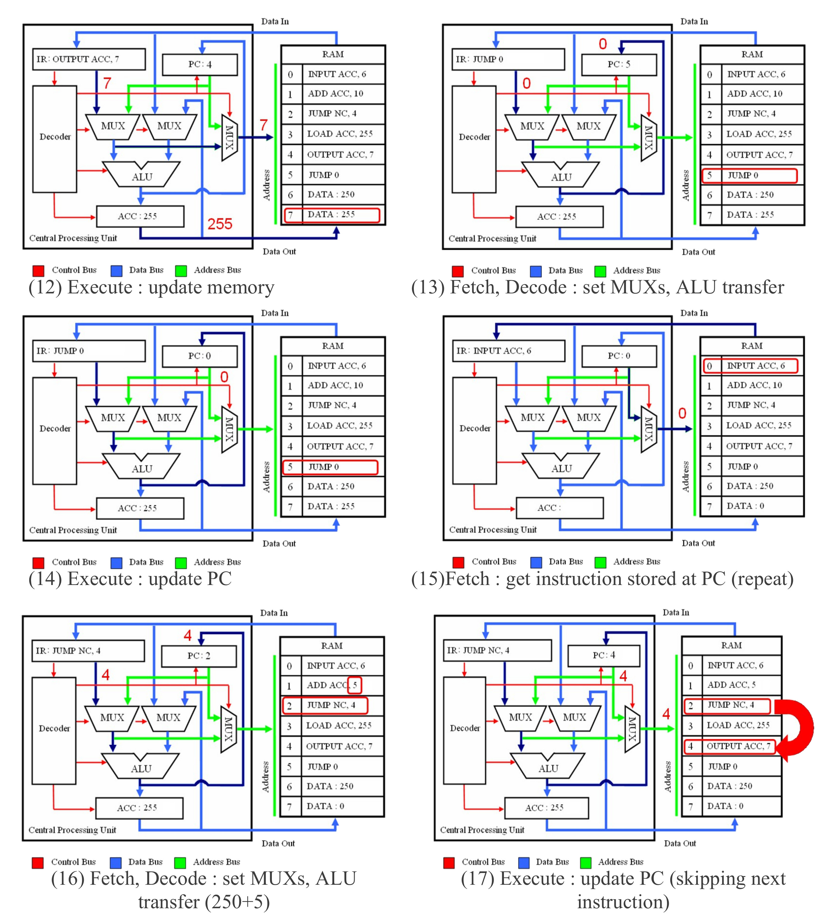
Figure 37 : steps 12 to 17
The memory used in the system (figure 38) stores both instructions and data i.e. a Von Neumann architecture. This could be constructed from the built in memory components used in the FPGA, but they are a real pain to configure i.e. initialise with the instructions (machine code) and data values needed. Therefore, i decided to cheat and use a bit of VHDL. This is a Hardware Description Language (HDL) representation of what the memory should do, abstracting away from the low level logic gates its actually made from. This allows me to simply type in the binary values as shown in figure 39. Note, i've only shown the first few values. This description is then synthesised (converted) by the Xilinx tools into the required hardware components. The complete computer system is shown in figure 40. A high resolution diagram can be downloaded here: (Link ).
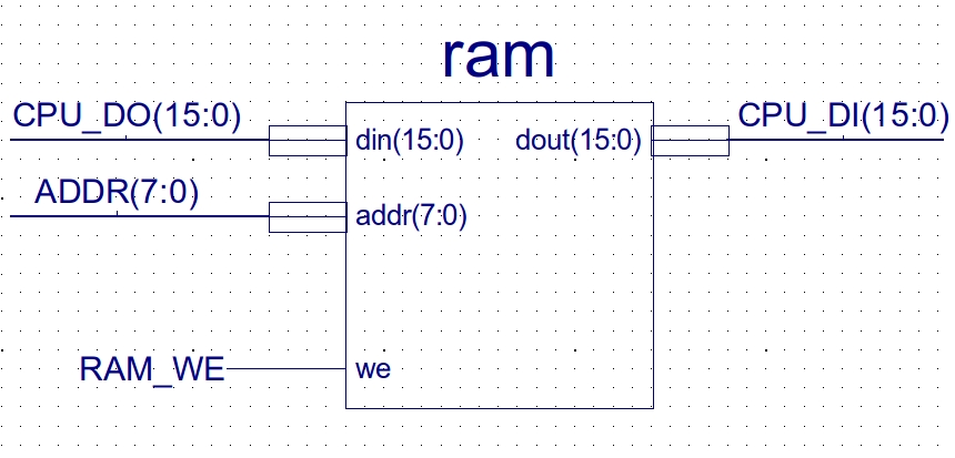
Figure 38 : RAM
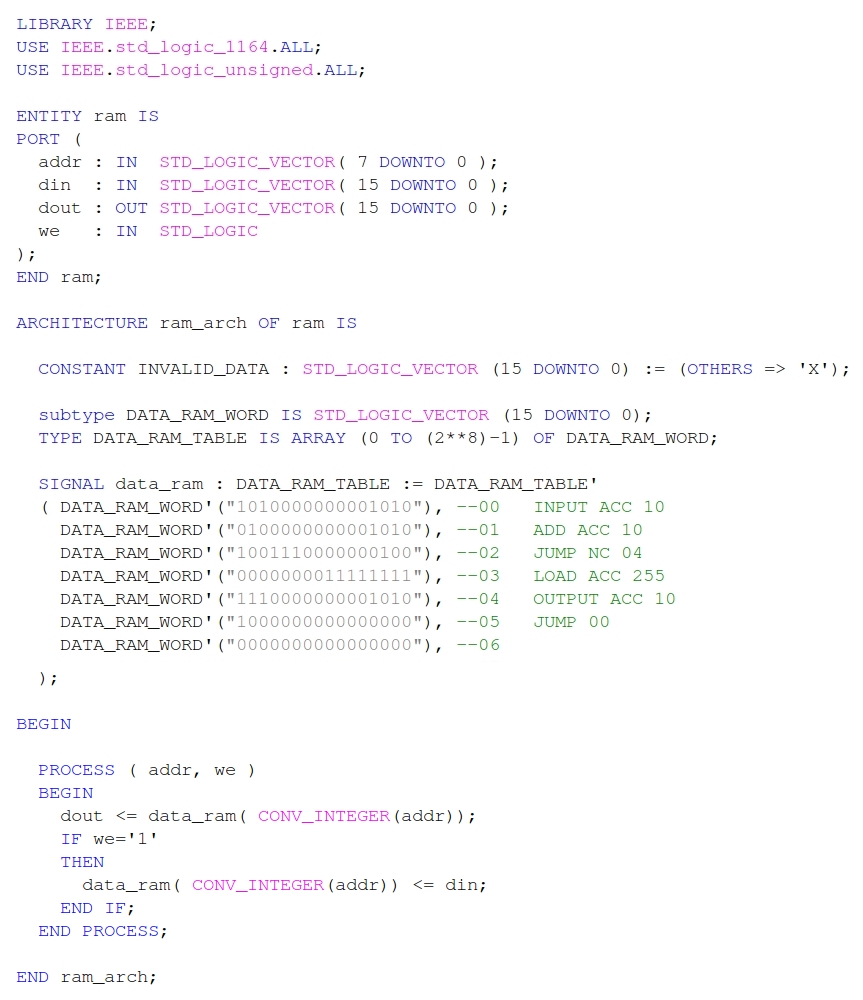
Figure 39 : VHDL (asynchronous, later modified to be synchronous)
The test program shown in figure 38 (machine code, comments on the right in green), loads the value stored in memory location 10 and adds 10 to it (decimal 10, not binary 10). If this does not generate an overflow i.e. a value larger than 255, the result is written back to memory location 10. If it does generate an overflow i.e. 250+10, the value is saturated to the maximum value i.e. 255. Therefore, program counts from 0 to 250 and then stops, as shown in the simulation shown in figure 41, look at the bottom row, this shows the contents of memory location 10 as a hexadecimal value (base 16). Note, the Xilinx schematics, symbols and VHDL testbench for the complete system can be downloaded using the links below (in next section). Have a play, modify the data values or write your own program, then re-run the simulation (top_level_v1_tb).
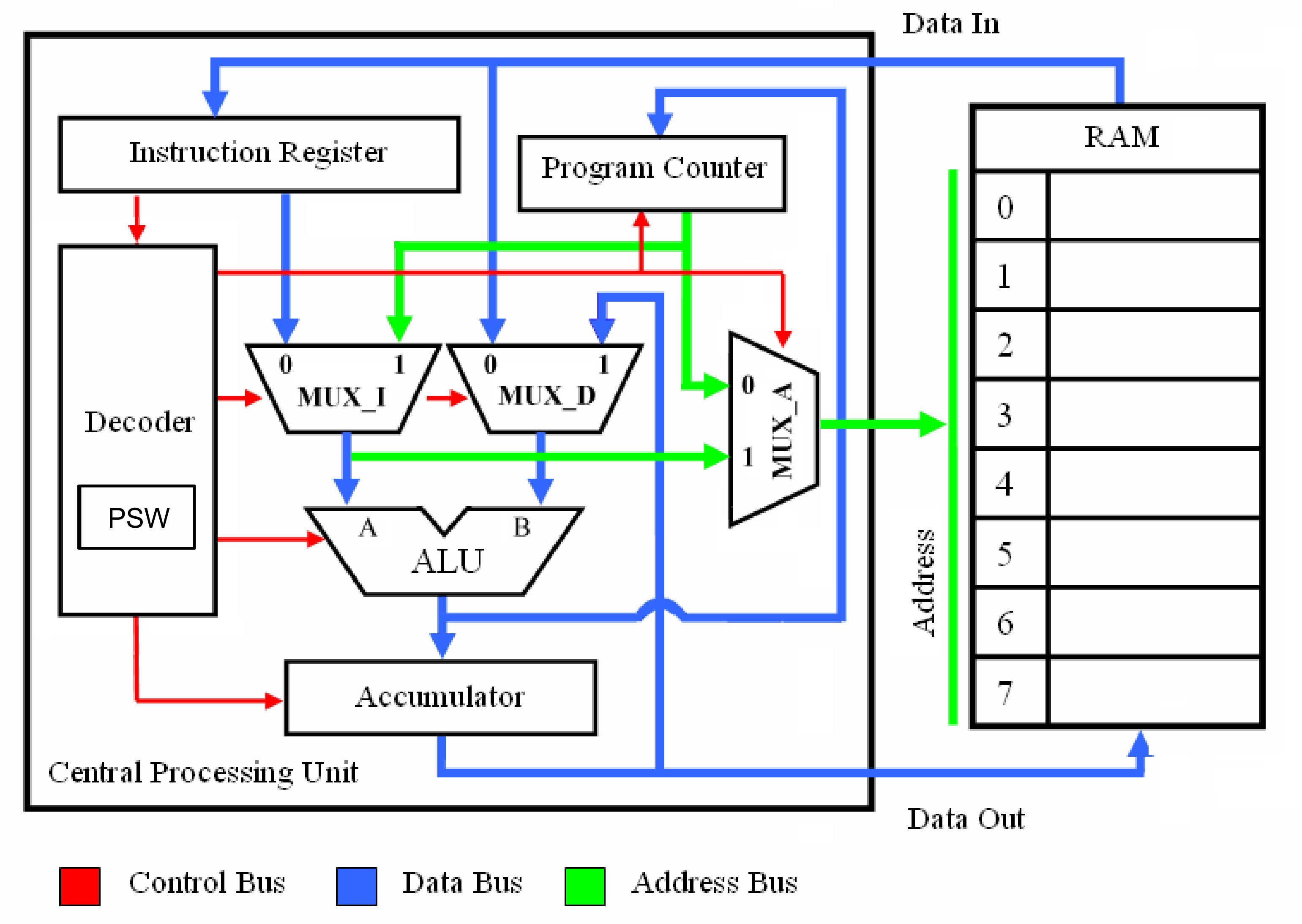

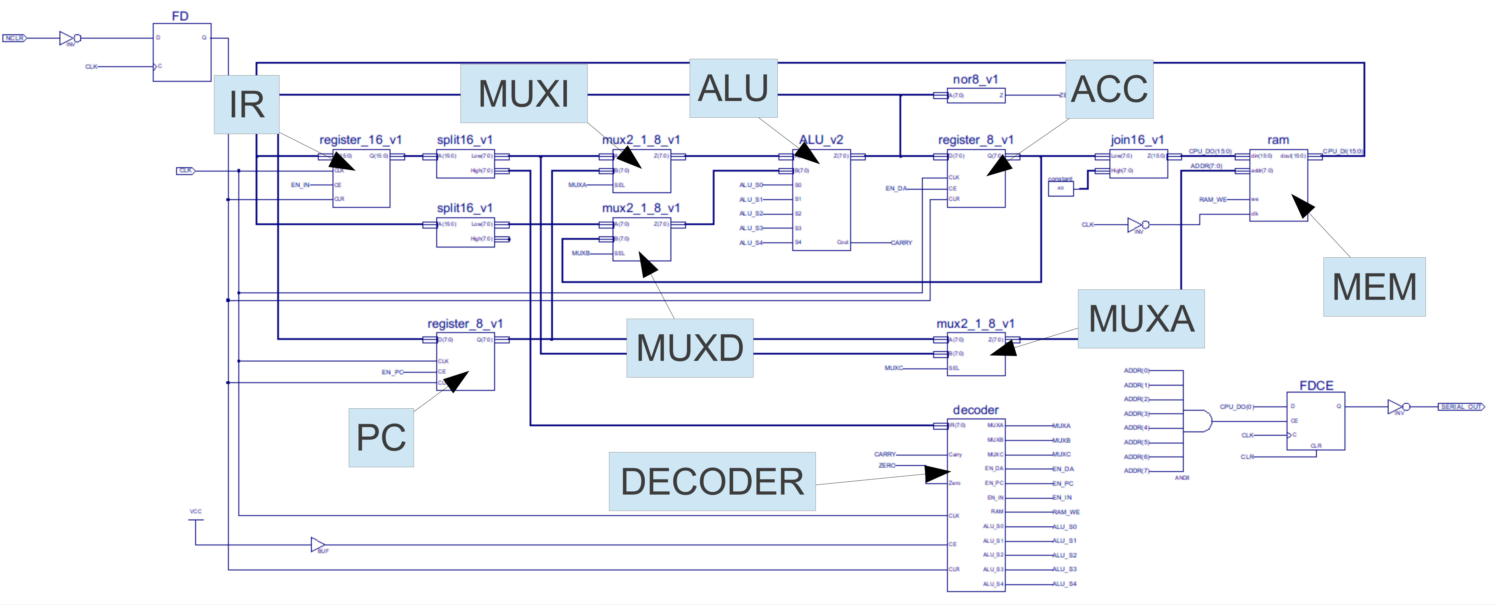
Figure 40 : Complete system
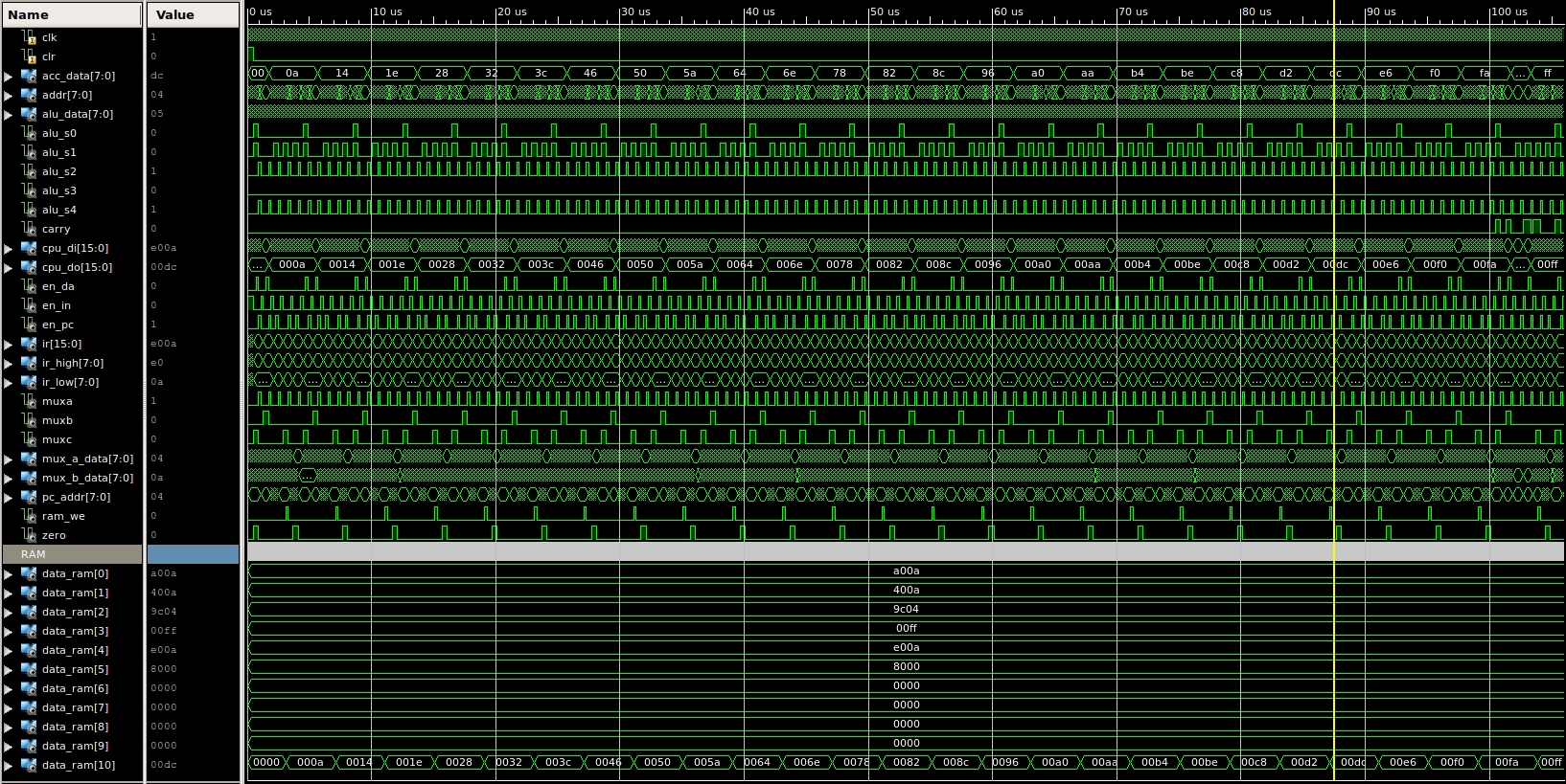
Figure 41 : Test program simulation
An interesting design point that i do confess ive skipped over for the moment is how the computer's memory is organised. The simpleCPU uses a Von Neumann architecture, therefore, instructions and data are stored in the same memory. This causes a conflict regarding a memory location's width i.e. how many bits are stored in each location, as instructions are 16bits and data is 8bit. The number of addressable memory locations is fixed by the address bus, in this case 8bits (256 location). This gives the designer a few choices:
A requirement when writing you first program on any new processor is to print "HELLO WORLD" to the screen. Normally a simple task, however, for a processor with no screen and only seven basic instructions a little more of a challenge. The simplest way to add a screen is to use a serial terminal (Link)(Link), then bit-bang out serial data packets (Link). However, you first need an output port, as shown in figure 42. This is simply a flip-flop who's CE pin is only enabled for a specific address, in this example address 0xFF (255). When data is written to this address (using an OUTPUT instruction), RAM is updated as normal, but, data bit 0 is also stored in this flip-flop, its Q output being connected to the transmit (TX) line of a serial bus.
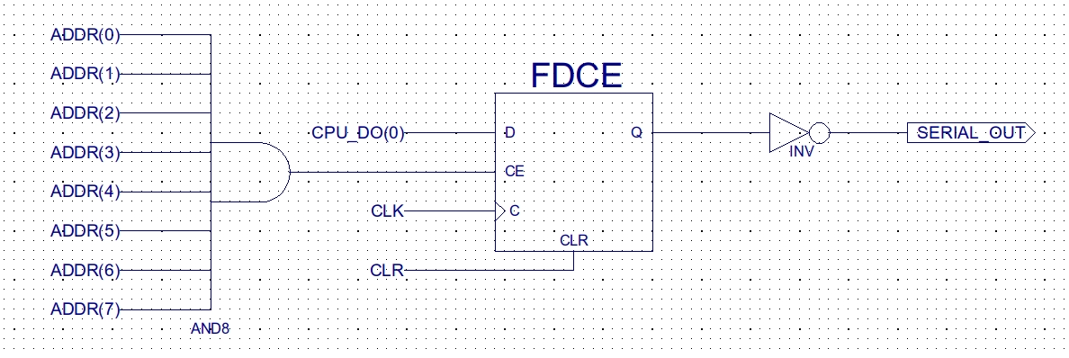
Figure 42 : Serial Output port
Each character in the "HELLO WORLD" message string is stored in memory, locations 0xF0 to 0xFD, as an ASCII value (Link). To simplify the program they are actually stored as their inverted forms e.g. H = 0x48 (01001000), inverted = 0xB7 (10110111). The program reads each character's bits and outputs these on the serial port. The serial data packet format for the character 'K' (0x4B = 01001011) is shown in figure 43 (Link). Each bit is allocated a time slice on the serial port's line. The default speed for the serial port is 9600 bits per second i.e. each bit is valid for 104 us (1/9600), packets start with a start bit (1) and finish with a stop bit (0). These packets are received by a terminal program running on a remote computer and displayed on its screen. The serial packets and terminal display are shown in figures 43 - 46.

Figure 43 : Serial packet format (wiki link above)
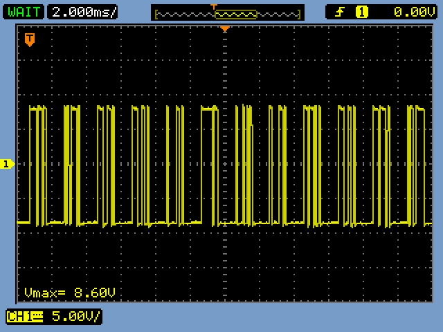
Figure 44 : HELLO WORLD serial packet (captured on scope)
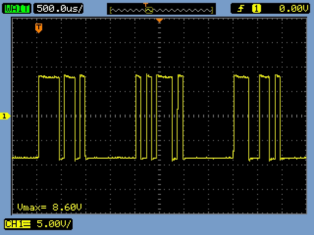
Figure 45 : First three characters "HEL" (captured on scope)
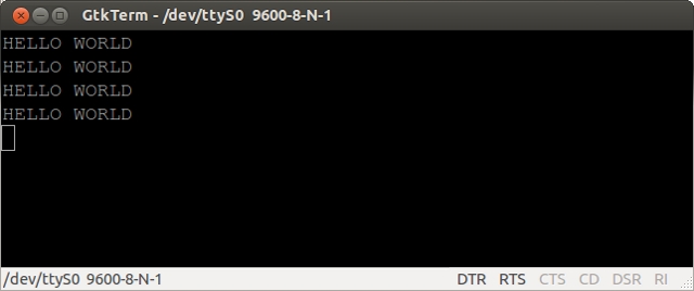
Figure 46 : Complete message displayed in terminal
The program to send the message string "HELLO WORLD" to the serial terminal is shown below. Hopefully most of the code is self explanatory :). The next character to be transmitted is read from memory location 0xE0, a bit mask is applied using a bitwise AND to select the desired bit. Based on this result a conditional jump then selects a 0 or a 1, which is stored to memory location 0xFF i.e. the output port (serial bit). This is repeated seven more times until all eight character bits have been outputted. The program below could of been substantially reduced if a SHIFT instruction had been included. The final twist is how the program scans through the message string. As this processor does not support indirect addressing modes, self modifying code (Link) is used to access the next character in the string i.e. instructions from 0x4F to 0x58. The program reads an INPUT instruction from memory, it then adds 1 to this instruction. As the INPUT instruction's address field is in the lower byte this changes the address that would be read to the address of the next character in the string. This modified instruction is then written back to memory and executed by the program. It goes without saying that self modifying coded i.e. a program that rewrites itself is not a good idea, however, its very useful in this case. Note, in early computer this was actually how the first subroutines i.e. functions, were implemented on EDSAC. The program then fetches the next character, storing it to memory location 0xE0, if this is a NULL (the value 0) the program finishes, otherwise the program jumps to memory location 0x02 and repeats the TX code. From a software structure point of view would of been nice if the processor had supported subroutines, perhaps for version 2.
    DATA_RAM_WORD'("1010000011110000"), --00   INPUT ACC 0xF0  - load first char
    DATA_RAM_WORD'("1110000011100000"), --01   OUTPUT ACC 0xE0 - update tx memory
    DATA_RAM_WORD'("0000000000000001"), --02   LOAD ACC 1      - Start Bit
    DATA_RAM_WORD'("1110000011111111"), --03   OUTPUT ACC 0xFF - Set serial port high
    DATA_RAM_WORD'("0000000011001110"), --04   LOAD ACC 0xCE   - wait loop (104us)
    DATA_RAM_WORD'("0100000000000001"), --05   ADD ACC 1       - Increment count
    DATA_RAM_WORD'("1001110000000101"), --06   JUMP NC 0x05    - repeat 50 times
    DATA_RAM_WORD'("1010000011100000"), --07   INPUT ACC 0xE0  - read character
    DATA_RAM_WORD'("0001000000000001"), --08   AND ACC 0X01    - mask bit0
    DATA_RAM_WORD'("1001000000001011"), --09   JUMP Z 0x0B     - if zero output
    DATA_RAM_WORD'("0000000000000001"), --0A   LOAD ACC 1      - else set 1
    DATA_RAM_WORD'("1110000011111111"), --0B   OUTPUT ACC 0xFF - Set serial port bit
    DATA_RAM_WORD'("0000000011001110"), --04   LOAD ACC 0xCE   - wait loop (104us)
    DATA_RAM_WORD'("0100000000000001"), --0D   ADD ACC 1       - Increment count
    DATA_RAM_WORD'("1001110000001101"), --0E   JUMP NC 0x0D    - repeat 50 times
    DATA_RAM_WORD'("1010000011100000"), --0F   INPUT ACC 0xE0  - read character

    DATA_RAM_WORD'("0001000000000010"), --10   AND ACC 0X02    - mask bit1
    DATA_RAM_WORD'("1001000000010011"), --11   JUMP Z 0x13     - if zero output
    DATA_RAM_WORD'("0000000000000001"), --12   LOAD ACC 1      - else set 1
    DATA_RAM_WORD'("1110000011111111"), --13   OUTPUT ACC 0xFF - Set serial port bit
    DATA_RAM_WORD'("0000000011001110"), --04   LOAD ACC 0xCE   - wait loop (104us)
    DATA_RAM_WORD'("0100000000000001"), --15   ADD ACC 1       - Increment count
    DATA_RAM_WORD'("1001110000010101"), --16   JUMP NC 0x15    - repeat 50 times
    DATA_RAM_WORD'("1010000011100000"), --17   INPUT ACC 0xE0  - read character
    DATA_RAM_WORD'("0001000000000100"), --18   AND ACC 0X04    - mask bit2
    DATA_RAM_WORD'("1001000000011011"), --19   JUMP Z 0x1B     - if zero output
    DATA_RAM_WORD'("0000000000000001"), --1A   LOAD ACC 1      - else set 1
    DATA_RAM_WORD'("1110000011111111"), --1B   OUTPUT ACC 0xFF - Set serial port bit
    DATA_RAM_WORD'("0000000011001110"), --04   LOAD ACC 0xCE   - wait loop (104us)
    DATA_RAM_WORD'("0100000000000001"), --1D   ADD ACC 1       - Increment count
    DATA_RAM_WORD'("1001110000011101"), --1E   JUMP NC 0x1D    - repeat 50 times
    DATA_RAM_WORD'("1010000011100000"), --1F   INPUT ACC 0xE0  - read character

    DATA_RAM_WORD'("0001000000001000"), --20   AND ACC 0X08    - mask bit3
    DATA_RAM_WORD'("1001000000100011"), --21   JUMP Z 0x23     - if zero output
    DATA_RAM_WORD'("0000000000000001"), --22   LOAD ACC 1      - else set 1
    DATA_RAM_WORD'("1110000011111111"), --23   OUTPUT ACC 0xFF - Set serial port bit
    DATA_RAM_WORD'("0000000011001110"), --04   LOAD ACC 0xCE   - wait loop (104us)
    DATA_RAM_WORD'("0100000000000001"), --25   ADD ACC 1       - Increment count
    DATA_RAM_WORD'("1001110000100101"), --26   JUMP NC 0x25    - repeat 50 times
    DATA_RAM_WORD'("1010000011100000"), --27   INPUT ACC 0xE0  - read character
    DATA_RAM_WORD'("0001000000010000"), --28   AND ACC 0X10    - mask bit4
    DATA_RAM_WORD'("1001000000101011"), --29   JUMP Z 0x2B     - if zero output
    DATA_RAM_WORD'("0000000000000001"), --2A   LOAD ACC 1      - else set 1
    DATA_RAM_WORD'("1110000011111111"), --2B   OUTPUT ACC 0xFF - Set serial port bit
    DATA_RAM_WORD'("0000000011001110"), --04   LOAD ACC 0xCE   - wait loop (104us)
    DATA_RAM_WORD'("0100000000000001"), --2D   ADD ACC 1       - Increment count
    DATA_RAM_WORD'("1001110000101101"), --2E   JUMP NC 0x2D    - repeat 50 times
    DATA_RAM_WORD'("1010000011100000"), --2F   INPUT ACC 0xE0  - read character

    DATA_RAM_WORD'("0001000000100000"), --30   AND ACC 0X20    - mask bit5
    DATA_RAM_WORD'("1001000000110011"), --31   JUMP Z 0x33     - if zero output
    DATA_RAM_WORD'("0000000000000001"), --32   LOAD ACC 1      - else set 1
    DATA_RAM_WORD'("1110000011111111"), --33   OUTPUT ACC 0xFF - Set serial port bit
    DATA_RAM_WORD'("0000000011001110"), --04   LOAD ACC 0xCE   - wait loop (104us)
    DATA_RAM_WORD'("0100000000000001"), --35   ADD ACC 1       - Increment count
    DATA_RAM_WORD'("1001110000110101"), --36   JUMP NC 0x35    - repeat 50 times
    DATA_RAM_WORD'("1010000011100000"), --37   INPUT ACC 0xE0  - read character
    DATA_RAM_WORD'("0001000001000000"), --38   AND ACC 0X40    - mask bit6
    DATA_RAM_WORD'("1001000000111011"), --39   JUMP Z 0x3B     - if zero output
    DATA_RAM_WORD'("0000000000000001"), --3A   LOAD ACC 1      - else set 1
    DATA_RAM_WORD'("1110000011111111"), --3B   OUTPUT ACC 0xFF - Set serial port bit
    DATA_RAM_WORD'("0000000011001110"), --04   LOAD ACC 0xCE   - wait loop (104us)
    DATA_RAM_WORD'("0100000000000001"), --3D   ADD ACC 1       - Increment count
    DATA_RAM_WORD'("1001110000111101"), --3E   JUMP NC 0x3D    - repeat 50 times
    DATA_RAM_WORD'("1010000011100000"), --3F   INPUT ACC 0xE0  - read character

    DATA_RAM_WORD'("0001000010000000"), --40   AND ACC 0X80    - mask bit7
    DATA_RAM_WORD'("1001000001000011"), --41   JUMP Z 0x43     - if zero output
    DATA_RAM_WORD'("0000000000000001"), --42   LOAD ACC 1      - else set 1
    DATA_RAM_WORD'("1110000011111111"), --43   OUTPUT ACC 0xFF - Set serial port bit
    DATA_RAM_WORD'("0000000011001110"), --04   LOAD ACC 0xCE   - wait loop (104us)
    DATA_RAM_WORD'("0100000000000001"), --45   ADD ACC 1       - Increment count
    DATA_RAM_WORD'("1001110001000101"), --46   JUMP NC 0x45    - repeat 50 times
    DATA_RAM_WORD'("0000000000000000"), --47   LOAD ACC 0      - stop bit
    DATA_RAM_WORD'("1110000011111111"), --48   OUTPUT ACC 0xFF - Set serial port bit
    DATA_RAM_WORD'("0100000000000001"), --49   ADD ACC 1       - Increment count
    DATA_RAM_WORD'("1001110001001001"), --4A   JUMP NC 0x49    - repeat 256 times
    DATA_RAM_WORD'("0000000000000000"), --4B   LOAD ACC 0      - stop bit
    DATA_RAM_WORD'("1110000011111111"), --4C   OUTPUT ACC 0xFF - Set serial port bit
    DATA_RAM_WORD'("0100000000000001"), --4D   ADD ACC 1       - Increment count
    DATA_RAM_WORD'("1001110001001101"), --4E   JUMP NC 0x4D    - repeat 256 times
    DATA_RAM_WORD'("1010000001010010"), --4F   INPUT ACC 52    - read instruction

    DATA_RAM_WORD'("0100000000000001"), --50   ADD ACC 1       - increment address field
    DATA_RAM_WORD'("1110000001010010"), --51   OUT ACC 52      - update instruction
    DATA_RAM_WORD'("1010000011110000"), --52   INPUT ACC 0xF0  - execute instruction
    DATA_RAM_WORD'("1110000011100000"), --53   OUTPUT ACC 0xE0 - update tx memory
    DATA_RAM_WORD'("0001000011111111"), --54   AND ACC 0xFF    - is char NULL?
    DATA_RAM_WORD'("1001010000000010"), --55   JUMP NZ, 2      - no, TX
    DATA_RAM_WORD'("0000000011110000"), --56   LOAD ACC 0xF0   - restore original instruction
    DATA_RAM_WORD'("1110000001010010"), --57   OUT ACC 52
    DATA_RAM_WORD'("1000000001010110"), --58   JUMP 56         - yes, halt

    DATA_RAM_WORD'("0000000010110111"), --F0  H      = 0x48 inv 10110111
    DATA_RAM_WORD'("0000000010111010"), --F1  E      = 0x45 inv 10111010
    DATA_RAM_WORD'("0000000010110011"), --F2  L      = 0x4C inv 10110011
    DATA_RAM_WORD'("0000000010110011"), --F3  L      = 0x4C inv 10110011
    DATA_RAM_WORD'("0000000010110000"), --F4  O      = 0x4F inv 10110000
    DATA_RAM_WORD'("0000000011011111"), --F5  'SP'   = 0x20 inv 11011111
    DATA_RAM_WORD'("0000000010101000"), --F6  W      = 0x57 inv 10101000
    DATA_RAM_WORD'("0000000010110000"), --F7  O      = 0x4F inv 10110000
    DATA_RAM_WORD'("0000000010101101"), --F8  R      = 0x52 inv 10101101
    DATA_RAM_WORD'("0000000010110011"), --F9  L      = 0x4C inv 10110011
    DATA_RAM_WORD'("0000000010111011"), --FA  D      = 0x44 inv 10111011
    DATA_RAM_WORD'("0000000011110010"), --FB  'CR'   = 0x0D inv 11110010
    DATA_RAM_WORD'("0000000011110101"), --FC  'LF'   = 0x0A inv 11110101
    DATA_RAM_WORD'("0000000000000000"), --FD  'NULL' = 0x00
    DATA_RAM_WORD'("0000000000000000"), --FE
    DATA_RAM_WORD'("0000000000000000")  --FF
Had to make a few small changes to the schematics and VHDL files to minimise the hardware size e.g. in its present form the memory is implemented by the software tools as a 256:1 16bit multiplexer, which takes up quite a bit of space. Adding a clock allows the memory to be mapped to a BlockRam i.e. the default RAM on the FPGA. The final project that prints "HELLO WORLD" can be downloaded here: (Link). NOTE: this version has 'errors' corrected version below.
What next for this computer, i want to see if i can get it to fit into a Xilinx 9572 CPLD, which we use for teaching hardware design, would need to use external RAM/ROM, however, the main limitation is that this programmable hardware only has a very small amount of hardware e.g. 72 flip-flops. Update, gave up on this idea mostly due to component sourcing issues for the RAM and EPROMs needed for the instruction and data memory.
Originally this processor was a quick case study, used a to illustrate the process of realising a simple processor architecture from Boolean logic gates. Do confess i only tested the hardware enough to get the "Hello World" case study working, as a result i didn't check that all the instructions worked correctly :). Received an email asking for some more detail / explanations about the operation of this processor, i suspect because there were some typos / errors, so i thought i better do a "full" test. The instruction set for this machine is:
Therefore, the test code below should allow me to test "all" the instructions:
    DATA_RAM_WORD'("0000000000000001"), --00   LOAD ACC 0x01     -
    DATA_RAM_WORD'("0100000000000000"), --01   ADD ACC, 0x00     - test NZ NC ACC=1
    DATA_RAM_WORD'("0100000011111111"), --02   ADD ACC, 0xFF     - test Z  C  ACC=0
    DATA_RAM_WORD'("0000000010101010"), --03   LOAD ACC 0xAA     -
    DATA_RAM_WORD'("0001000000001111"), --04   AND ACC, 0x0F     - test NZ NC ACC=0x0A
    DATA_RAM_WORD'("0001000000000000"), --05   AND ACC, 0x00     - test Z  NC ACC=0x00
    DATA_RAM_WORD'("0000000000000001"), --06   LOAD ACC 0x01     -
    DATA_RAM_WORD'("0110000000000001"), --07   SUB ACC, 0x01     - test Z  NC ACC=0x00
    DATA_RAM_WORD'("0110000000000001"), --08   SUB ACC, 0x01     - test NZ C  ACC=0xFF
    DATA_RAM_WORD'("1110000011110000"), --09   OUTPUT ACC, 0xF0  - test M[0xF0] = 0xFF
    DATA_RAM_WORD'("0000000000000000"), --0A   LOAD ACC 0x00     -
    DATA_RAM_WORD'("1010000011110000"), --0B   INPUT ACC, 0xF0   - test ACC = 0xFF
    DATA_RAM_WORD'("0100000000000000"), --0C   ADD ACC, 0x00     - test NZ NC ACC=0x01
    DATA_RAM_WORD'("1001010000001111"), --0D   JUMP NZ, 0x0F     - skip trap if correct
    DATA_RAM_WORD'("1000000000001110"), --0E   JUMP 0x0E         - trap
    DATA_RAM_WORD'("0100000000000001"), --0F   ADD ACC, 0x01     - test Z NC ACC=0x00
    DATA_RAM_WORD'("1001000000010010"), --10   JUMP Z, 0x12      - skip trap if correct
    DATA_RAM_WORD'("1000000000010001"), --11   JUMP 0x11         - trap
    DATA_RAM_WORD'("0000000000000010"), --12   LOAD ACC 0x02
    DATA_RAM_WORD'("0100000011111111"), --13   ADD ACC, 0xFF     - test NZ C ACC=0x01
    DATA_RAM_WORD'("1001100000010110"), --14   JUMP C, 0x16      - skip trap if correct
    DATA_RAM_WORD'("1000000000010101"), --15   JUMP 0x15         - trap
    DATA_RAM_WORD'("0110000000000001"), --16   SUB ACC, 0x01     - test Z  NC ACC=0x00
    DATA_RAM_WORD'("1001100000011001"), --17   JUMP NC, 0x19     - skip trap if correct
    DATA_RAM_WORD'("1000000000011000"), --18   JUMP 0x15         - trap
    DATA_RAM_WORD'("1000000000000000"), --19   JUMP 0x00         - loop
This is not a full test of all functional units, with all possible data values, or all possible combinations of instructions, as this would take forever, but this code does test typical usage so should highlight any major issues. Testing start ok, LOAD, AND, ADD all seemed to work ok, then i came to the SUB instruction :(. I had missed off the ACC update, also messed up MUX_A and MUX_B. For ADD and AND it doesn't matter which way round the operands are passed to the ALU e.g. (ACC=InputA, Constant=InputB) or (ACC=InputB, Constant=InputA), both will produce the same result. Subtraction however, we need (ACC - Constant), performing the subtraction the other way round is not that helpful :(. This was "easy" to fixed i.e. switch over the data paths from the ACC and IR to the two multiplexers, but this does mean i have to update the decoder logic and more annoyingly redraw all the block diagrams in the lecture slides, one day :). Therefore, switched the data buses and updated the decoder, now the ACC has the correct value, but, another joy did not consider the carry flag. The ALU performs subtract by the addition of a negative number, therefore, if ACC=1 subtracting 1 will set the carry flag as this operation is implemented by adding 255. At present not sure how to handle this one, i feel there is a simple solution shouting at me, but, for the moment going for the tried and tested approach of ignoring it :). The new and improved SimpleCPU project files and this test code can be downloaded here: (Link).

This work is licensed under a Creative Commons Attribution-NonCommercial-NoDerivatives 4.0 International License.
Contact email: mike@simplecpudesign.com