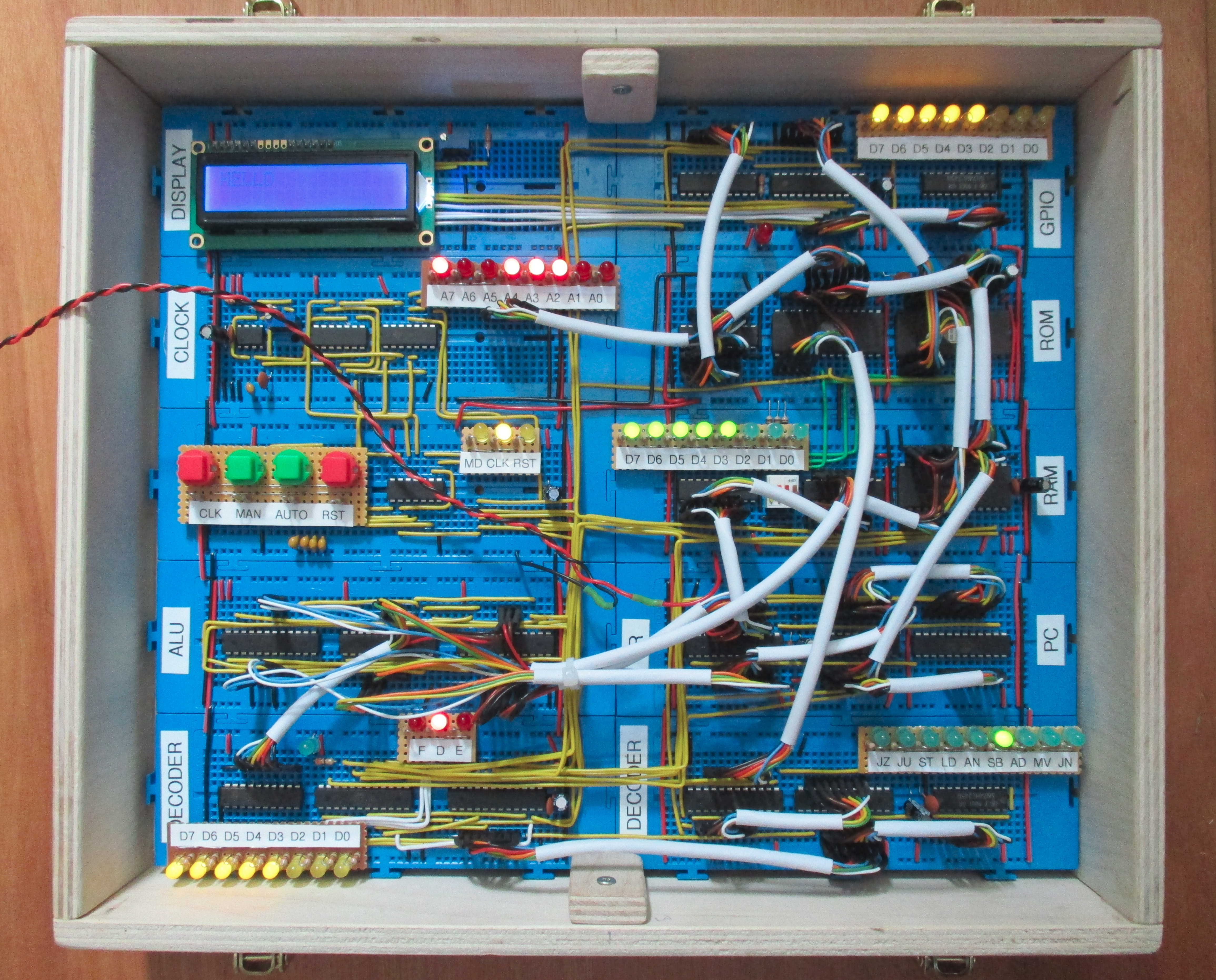
Figure 1 : simpleCPU v1a implemented on bread boards
To help demonstrate the operation of a SimpleCPU based computer i.e. the different phases performed during an instruction's execution and the movement of information through the machine, i decided to build this architecture on bread board, as shown in figure 1. This gives students a real view of the complexities of actually building a processor that are just hidden from view in the previous FPGA implementations i.e WIRES, WIRES and more WIRES :). Originally i was going to build this using the classic 7400 series logic gates (Link), but to try and keep the build size down to something that i could reliably transport between lectures i decided to implement some of the more complex logic circuits in Simple Programmable Logic Devices (SPLDs). I know you could argue that this defeats the point a little i.e. you are hiding details in ICs again, but this approach still allows me to break the different architectural units down into different ICs, allowing people to 'see' what is connected to what i.e. how the block diagram in figure 2 is converted into the actual hardware shown in figure 1. A short video of the computer running its first test program is available here: (Video).
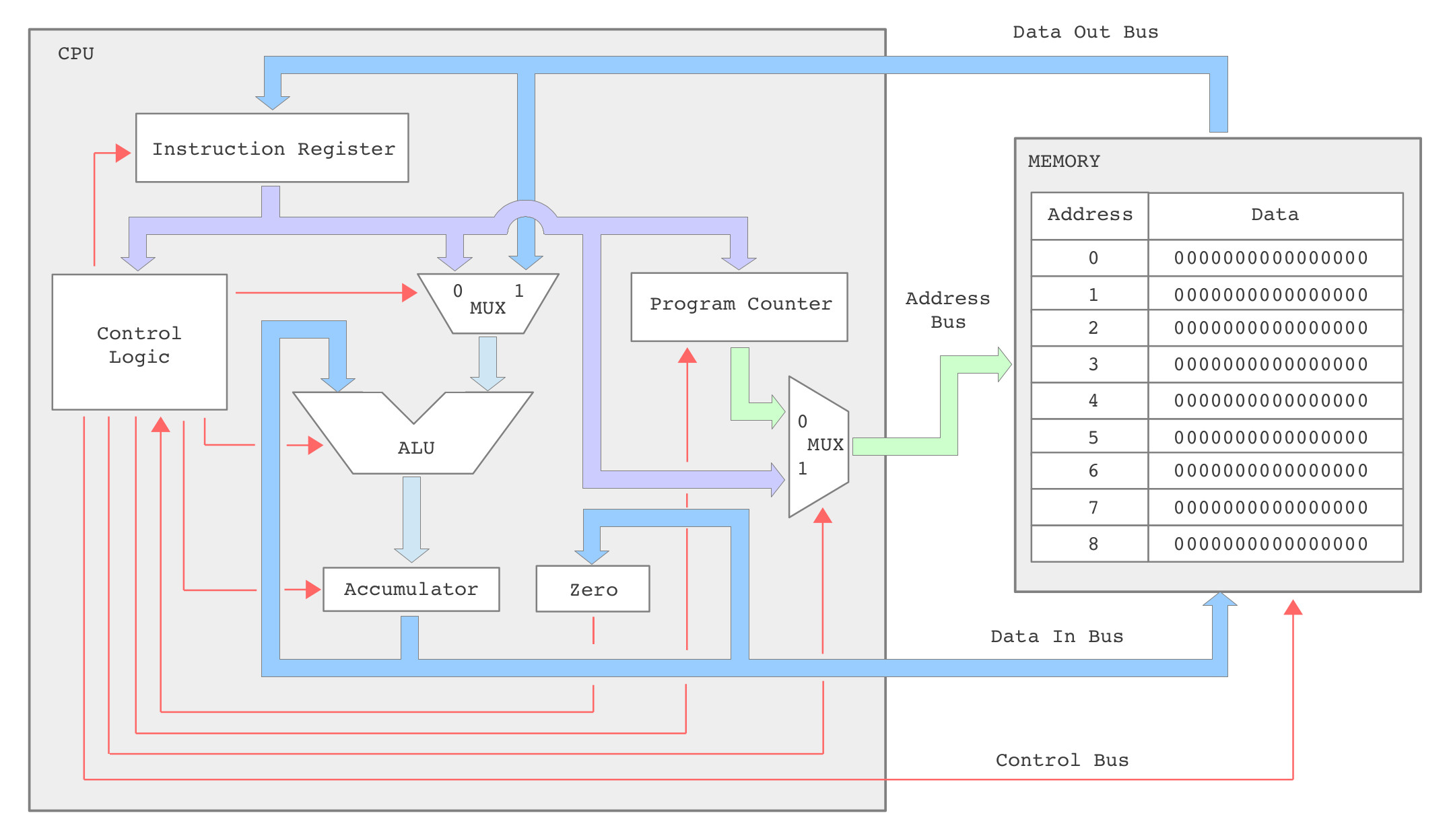
Figure 2 : simpleCPU v1a architecture
To simplify hardware construction this version of the processor only has a very limited instruction set, supporting 9 different instructions, shown below (assembly-code : machine-code). Note, decided to move away from the PicoBlaze syntax used in the original and return to the more typical usage of LOAD and STORE :)
In this instruction syntax X=Not-used, K=Constant and A=Address. The complexity of an instruction is also defined by its addressing mode i.e. not just how much number crunching it does, but how it fetches its operands (data). Again, to simplify the required hardware these instructions are limited to simple addressing modes:
Simple Programmable Logic Devices
Clock and Reset circuits
Instruction Register (IR)
Program Counter (PC)
Read Only Memory (ROM)
Random Access Memory (RAM)
Arithmetic and Logic Unit (ALU)
Control Logic (DECODER)
General Purpose Input/Output (GPIO)
Display
Final System
Improvements :)
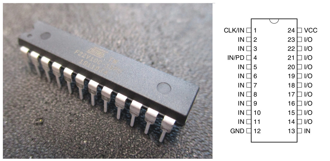
Figure 3 : SPLD - ATF22V10C
Before the development of the FPGA these were your goto ICs, used to help reduce hardware development times i.e before system on a chip (SoC), when PCB and pin through hole where king. They are still handy devices if you want a small simple custom IC and relatively cheap, they are also EEPROM rather than RAM based, so you don't need to keep re-configuring them when you do a power cycle i.e. they keep their configuration, unlike FPGAs. For this design i used two ICs from Atmel the ATF22V10C (Datasheet) and ATF16V8CZ (Datasheet). Internally they are configured as a big AND gate array feeding OR/XOR gates that can either be used to drive a D-type flop-flop or directly drive an output pin if you just need logic, as shown in figures 4.

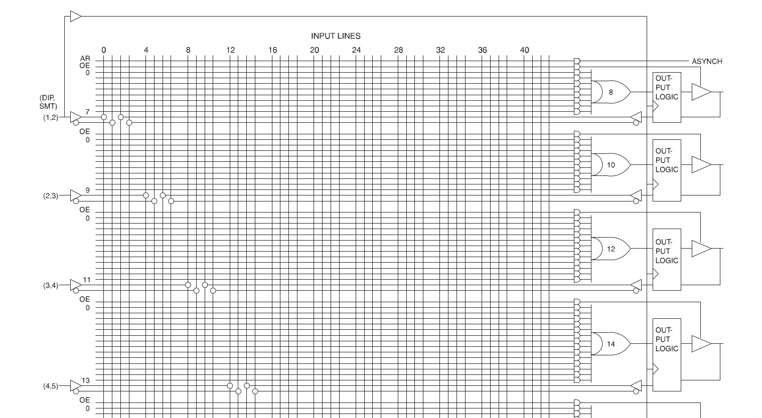
Figure 4 : SPLD architecture, overview (top), internal (bottom)
The bottom image in figure 4 shows the internal arrangement of the first four output pins, you have ten outputs in the ATF22V10C and eight in the ATF16V8CZ. There are some small internal differences between these two devices, but basically they use the same architecture. Note, a gotcha is that the number of inputs to each OR gate varies, as shown in figure 4, these vary from 8 to 16, so you need to take this into consideration when assigning functionality to pins. Therefore, the ATF22V10C can be configured to be "any" 11 input, 10 output logic circuit, if only this was true :), you do need to take into account the internal architecture and design your circuit accordingly, normally you are limited by the number of OR/XOR gates available, so where possible you try and use AND gate biased implementations, clocks and clears also need to be a considered as they are typically assigned to specific pins.
To configure these SPLDs you use the hardware description language: Compiler for Universal Programmable Logic (CUPL) (Link). As a language its ok, but i confess i prefer ABEL, but, CUPL is the language used by the Atmel tools used to configure these devices, so CUPL it is. You can download these tools from: (Link). This code converts the CUPL hardware description into a .jed file that can then be loaded into a programmer to configure the SPLDs. An introduction to the CUPL language is available here: (Link). Like any HDL the tools will allow you specify hardware designs that are not supported by the technology you are using, therefore, you need to keep an eye of the datasheets e.g. you can only have a single clock source, ten OR gates in the ATF22V10C etc. The tools come with some nice examples to get you started, a simple logic gate design is shown below:
Name            Gates;
Partno          CA0001;
Revision        04;
Date            9/12/89;
Designer        G. Woolhiser;
Company         Logical Devices, Inc.;
Location        None;
Assembly        None;
Device          g16v8a;

/****************************************************************/
/*                                                              */
/*      This is a example to demonstrate how CUPL               */
/*      compiles simple gates.                                  */
/*                                                              */
/****************************************************************/

/*
 * Inputs:  define inputs to build simple gates from
 */

Pin 1 =  a;
Pin 2 =  b;

/*
 * Outputs:  define outputs as active HI levels
 *
 */

Pin 12 = inva;
Pin 13 = invb;
Pin 14 = and;
Pin 15 = nand;
Pin 16 = or;
Pin 17 = nor;
Pin 18 = xor;
Pin 19 = xnor;

/*
 * Logic:  examples of simple gates expressed in CUPL
 */

inva = !a;              /* inverters */
invb = !b;
and  = a & b;           /* and gate */
nand = !(a & b);        /* nand gate */
or   = a # b;           /* or gate */
nor  = !(a # b);        /* nor gate */
xor  = a $ b;           /* exclusive or gate */
xnor = !(a $ b);        /* exclusive nor gate */
Like the analogue simulation language SPICE the title block is not optional this is part of the language. Comments are indicated by the /* */ notation. The first section defines pin names, some pins are input only, some are input-output (IO), so again you need to refer to the datasheet. Note, in this design we are not using flip-flops, therefore, pin 1 can be used as an input, normally this pin is reserved for the clock. In this design we are using a g16v8a, the generic name for a ATF16V8CZ, with pins 1 - 2 as inputs and 12 - 19 as outputs. Basic logic functions are defined using the following syntax:
To connect to the D-type flip-flops you need to use the "dot extensions" to specify particular flip-flop pins. CUPL defines a wide range of extensions, however, for the ATF22V10C devices only the following extensions are valid. To illustrate these consider the simple four bits counter below:
Name     Counter ;
PartNo   00 ;
Date     19/07/2019 ;
Revision 01 ;
Designer mike ;
Company  SimpleCPU ;
Assembly None ;
Location UK ;
Device   g22v10;

/**************** INPUT PINS **********************/
PIN 1  = clk ; /*  clock                          */
PIN 2  = ce  ; /*  chip enable      (active high) */
PIN 3  = ld  ; /*  load             (active high) */

PIN 8  = D3  ; /*  four bit output                */
PIN 9  = D2  ; /*                                 */
PIN 10 = D1  ; /*                                 */
PIN 11 = D0  ; /*                                 */

PIN 13 = clr ; /*  clear            (active high) */
PIN 14 = oe  ; /*  output enable    (active high) */

/**************** OUTPUT PINS *********************/

PIN 23 = Q0  ; /*  four bit input                 */
PIN 22 = Q1  ; /*                                 */
PIN 21 = Q2  ; /*                                 */
PIN 20 = Q3  ; /*                                 */

/***************** EQUATIONS **********************/

Q0.d = (Q0 & !ce & !clr) # (!Q0 & !ld & ce) # (D0 & ld & ce);
Q1.d = (Q1 & !ce & !clr) # ((Q1 $ Q0) & !ld & ce) # (D1 & ld & ce);
Q2.d = (Q2 & !ce & !clr) # ((Q2 $ (Q1 & Q0)) & !ld & ce) # (D2 & ld & ce);
Q3.d = (Q3 & !ce & !clr) # ((Q3 $ (Q2 & Q1 & Q0)) & !ld & ce) # (D3 & ld & ce);

/***************** GLOBAL  ************************/

Q0.oe = oe;
Q1.oe = oe;
Q2.oe = oe;
Q3.oe = oe;
As shown in figure 4 the SPLDs use a global clock connected to pin 1. On power-up all flip-flops are reset to zero, however, there is no external clear/reset line (CLR), or chip-enable line (CE), these have to be implemented from logic. The D input of the flip-flop is specified using the .d dot extension. From a comparable 7400 series hardware view point each flip-flop is configured using the circuit shown in figure 5. The D input of each flip-flop is driven by a three-input multiplexer, made from two two-input multiplexers: MUX_A and MUX_B. The first multiplexer MUX_A implements the CE functionality. All flip-flops share a common clock so will update each clock cycle, however, when CE=0 the current Q output is feed back by the MUX to the flip-flop's D input, such that the flip-flop updates its output with the current Q value i.e. will not change. When CE=1 the next count value or the associated D input is passed to the D input of the flip-flop via MUX_B. The CLR functionality is implemented by an AND gate, such that when CLR=1 the Q feedback is set to zero, setting the flip-flop output to 0 on the next clock cycle (synchronous clears only). The output enable functionality uses the .oe dot extension, when OE=0 the outputs Q0,Q1,Q2 and Q3 are disconnected from the output pins (tri-stated), when OE=1 they are driven by the flip-flops.
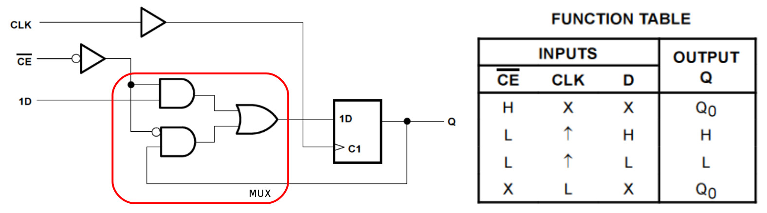
Figure 5 : Chip Enable : Basic circuit (top), Counter circuit (bottom)
Using a mixture of 7400 series logic, off the shelf standard ICs and SPLDs we can now construct the simpleCPU architecture on bread-board.
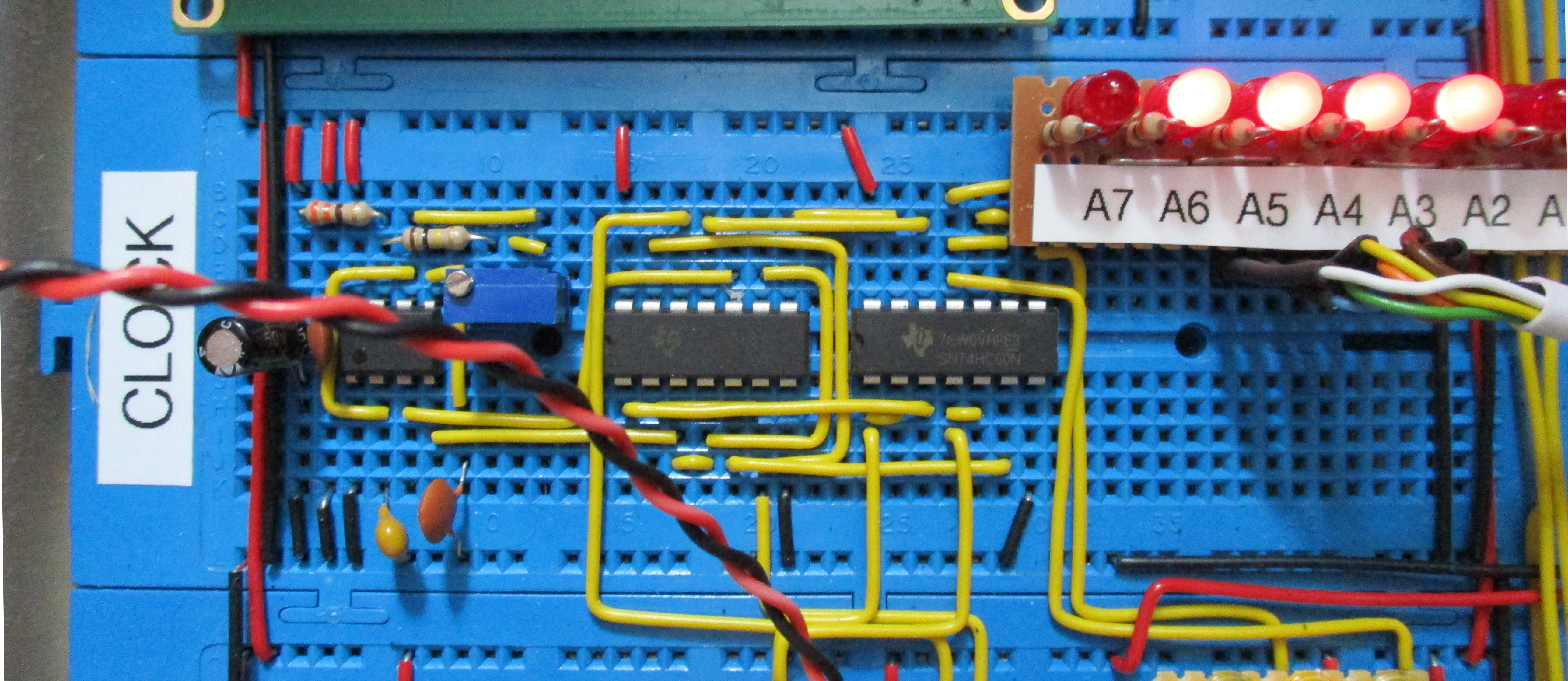
Figure 6 : Clock and reset bread-board
The internal phases of the processor are controlled using the system clock, a repeating square wave who's rising or falling edges co-ordinates the movement of information through the computer, as shown in figure 7. The clock signal's speed (period) is measured in seconds i.e. how long it takes to produce a pulse: a signal going from a logic 0 -> logic 1 -> logic 0. The number of pulses per second is the frequency measured in Hertz (Hz). Normally this clock signal is produced by a crystal oscillator, a very precise / stable square wave generator, producing a signal that changes millions of times per second e.g. a 100MHz clock will produce a pulse every 10ns. However, in this computer we want to see the state changes associated with each phase, therefore, we will be using a clock running at a slightly slower speed e.g. 1Hz to 5Hz, a signal that can be adjusted to produce 1 to 5-ish pulses per second. As this is a very slow clock a simple RC network can be used to generate this signal, as changes in output frequency owing to variations in R due to temperature will be very minimal, therefore, we can use a simple 555 timer astable multivibrator. For more information on this timer IC refer to: (Link), to calculate the values of R & C: (Link).
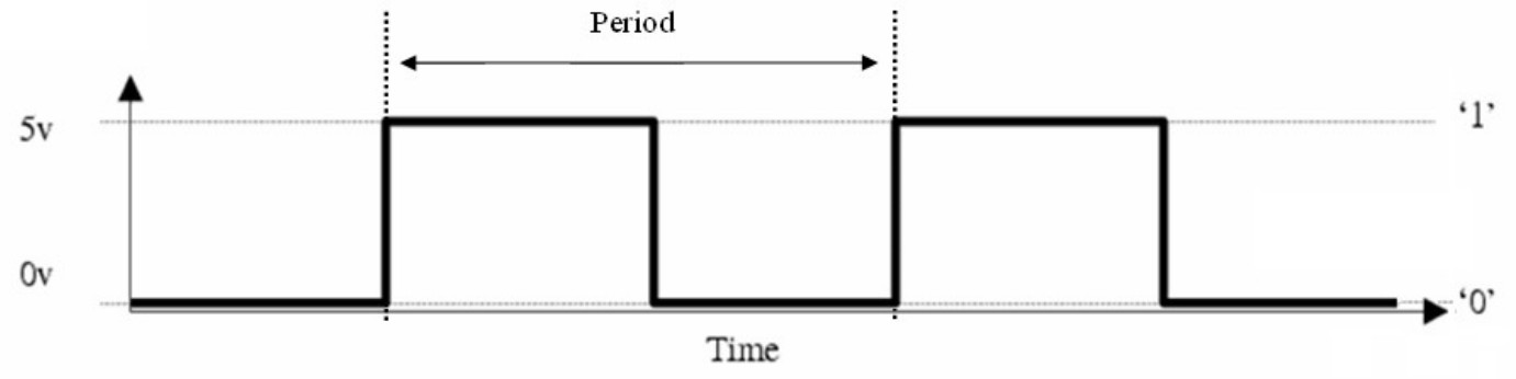
Figure 7 : System clock
The circuit used to control the computer's clock and reset signals is shown in figure 8.
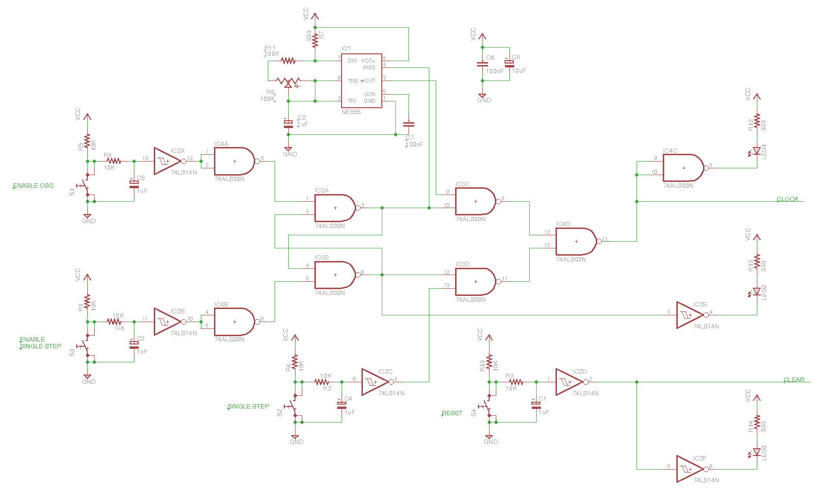
Figure 8 : Complete clock and reset circuit
The 555 timer circuit is shown in figure 9. This is a standard circuit, nothing special here. The only things to note is that the value of R1 (330) must be significantly small than R2 (100K + 200K variable). This ensures that the output duty cycle i.e. the time the signal is in a logic 1 and logic 0 states are roughly the same, 50:50 duty cycle. The output frequency can be varied be adjusting the variable resistor from 1Hz-ish to 7Hz. Note, value typo in schematic, variable resistor is 200K, the bigger the R the slower the clock.
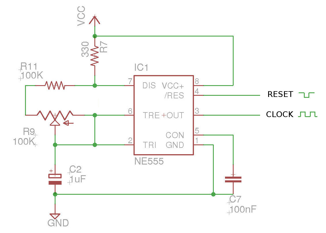
Figure 9 : 555 timer astable multivibrator
To allow me to show each phase of an instruction being executed i also need to be able to single step through a program i.e. manually generate a clock pulse each time a button is pressed. Therefore, we need a circuit to store the current operating mode: manual or automatic, and a circuit to generate a clean clock pulse each time a button is pressed. The problem is that switches can be quite electrically noisy i.e. produce multiple pulses each time they are pressed. This is due to the momentum of the switch contacts i.e. when you press a button the contacts are moved/closed, however, they do not stop instantaneously and will 'bounce' generating multiple open/close transitions until they settle down into their final closed position. For more information on contact bounce refer to: (Link). To remove any noise produced, a simple RC low pass filter combined with a Schmitt trigger inverter (Link) can be used, as shown in 10. For more information on switch debouncing refer to: (Link).
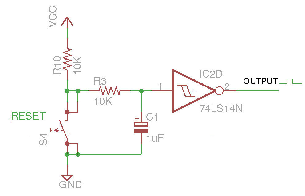
Figure 10 : RC switch debounce circuit
The computer has four switches as shown in figure 11. Mode selection: MAN / AUTO, clock: CLK and reset: RST. Each switch is passed through a debounce circuit like the one shown in figure 10. Note, strictly speaking the MAN / AUTO switches do not need to be debounced as they are used to control a SR flip-flop (discussed later), but it doesn't hurt to debounce them, just to make sure :).

Figure 11 : buttons
To remember the system's operating state i.e. AUTOMATIC or MANUAL clocking, we can use a simple Set / Reset (SR) flip-flop constructed from two NAND gates, in this case in a 7400 IC, as shown in figure 12.
Figure 12 : 7400 Quad NAND IC
The SR flip-flop is constructed from NAND gates 3A and 3B shown in figure 13. The inputs to the SR flip-flop are active low, however, the outputs from the debounce circuits are active high, therefore, NAND gates 4A and 4B are used as inverters to generate the active low signals required i.e. a two-input NAND gate with its inputs tied together becomes an inverter, consider the truth table below:
A B Z    A = B    A B Z
0 0 1             0 0 1
0 1 1             X X X
1 0 1             X X X
1 1 0             1 1 0
In operation if the set input (S) shown in figure 13 is pulsed high the Q output is set to a logic 1, the NOT_Q output to a logic 0. If the reset input (R) is pulsed high the Q output is set to a logic 0, the NOT_Q output to a logic 1. Holding this state until the S or R inputs are pulsed again. Note, this is why the MAN and AUTO buttons don't really need to be debounced as any pulses generated by contact bounce on the S or R inputs will only repeatedly set or repeatedly reset the flip-flop. For more information on how a SR flip-flop works refer to: (Link).
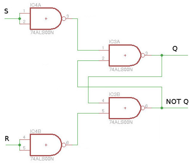
Figure 13 : SR flip-flop
The SR flip-flops outputs are used to control a multiplexer to select either the 555 timer's output or the debounced manual clock signal. To construct a two input multiplexer we would normally use the circuit shown in figure 14 (top), however, this would require three separate ICs: 7432 OR gate, 7404 NOT gate and a 7408 AND gate, taking up valuable space on the bread board. However, by using a little bit of Boolean algebra: DeMorgan's Theorem, we can actually implement this circuit from spare NAND gates, as shown in figure 14 (bottom).
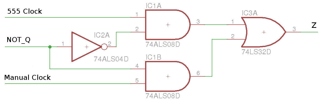
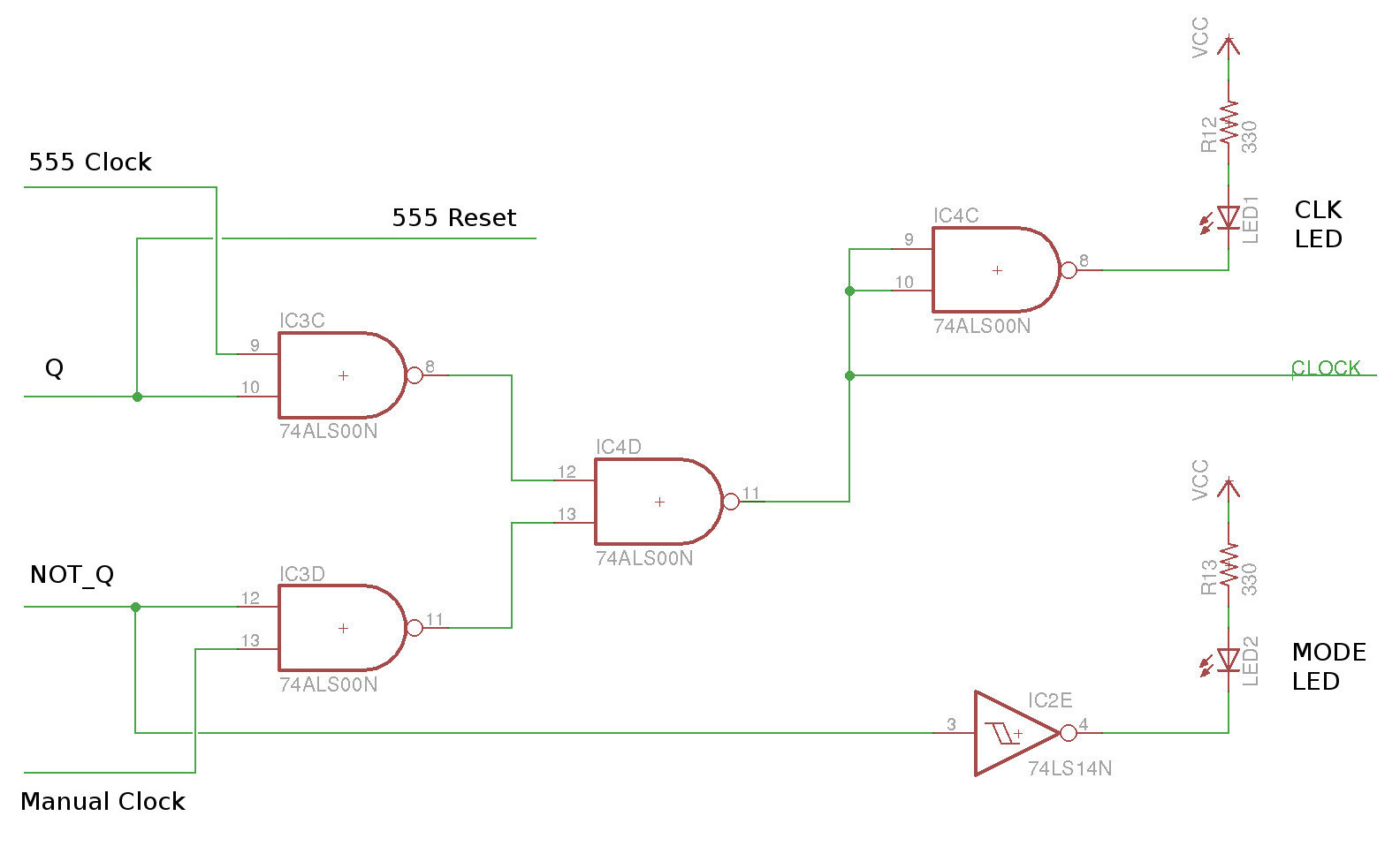
Figure 14 : "2:1 multiplexer, normal (top), NAND gate implementation (bottom)
A separate inverter is not required as the SR flip-flop produces both Q and NOT_Q. The two AND gates in the normal multiplexer implementation can be implemented by the NAND gates (ignoring their inversion for the moment), the OR gate is produced by the circuit shown in figure 15. Here the inverters from the NAND gates and their AND functions combine to produce the multiplexer's OR gate. When the SR flip-flop is set, Q=1 the 555 timer's output is selected, when the SR flip-flop is reset, Q=0 the manual debounced clock is selected, allowing the user to single step through the instruction phases. When Q=0 this signal also resets the 555 stopping the oscillator. This was done so that when you switch back to automatic you should start with a good clock pulse, rather than switching in half way through a pulse.
Figure 15 : DeMorgan's Theorem - converting OR gates to AND gates
Finally, the spare NAND and inverter gates are used to drive LED indicators, displaying the state of the MODE, CLOCK and RESET signals. These LEDs could be driven by the "raw" mode, clock and reset signals, but the current (I) needed to drive these LEDs places a significant load on the gates producing these signals and could increase the signals rise time (time it takes to go from a logic 0 to a logic 1), possibly increasing signal skew that may result in timing errors. As shown in figure 16, logic gates have a limited drive current, if you consider output power to be fixed i.e. given that P=VI, then if you exceed the maximum drive current the output voltage has to reduce, again possibly invalidating the signals noise margins i.e. reducing the voltage levels such that they are no longer recognised as a logic 1. Therefore, driving LEDs from signals that will be read by other logic gates is not the best idea.
Note, the thing to remember is that when you change the state of a signal i.e. from a logic 1 to 0, or from a logic 0 to 1, its all about moving electrons off and on wires. As shown in figure 16 in a normal test circuit wires are represented as a RL and CL load, so effectively when you change the state of a wire you are charging and discharging stray capacitance associated with wires and IC inputs. The speed at which this occurs is determined by the amount of current coming from the gate driving this wire, therefore, if your wasting this current driving an LED the speed at which this occurs slows down i.e. your square waves start to turn into "sine" waves, which is not what we want for digital systems.
Therefore, all LEDs in this computer are driven by separate driver/buffer ICs such that no significant load is placed on the original signals.
Figure 16 : Rise-Fall timing
Parts list for the clock reset circuits:
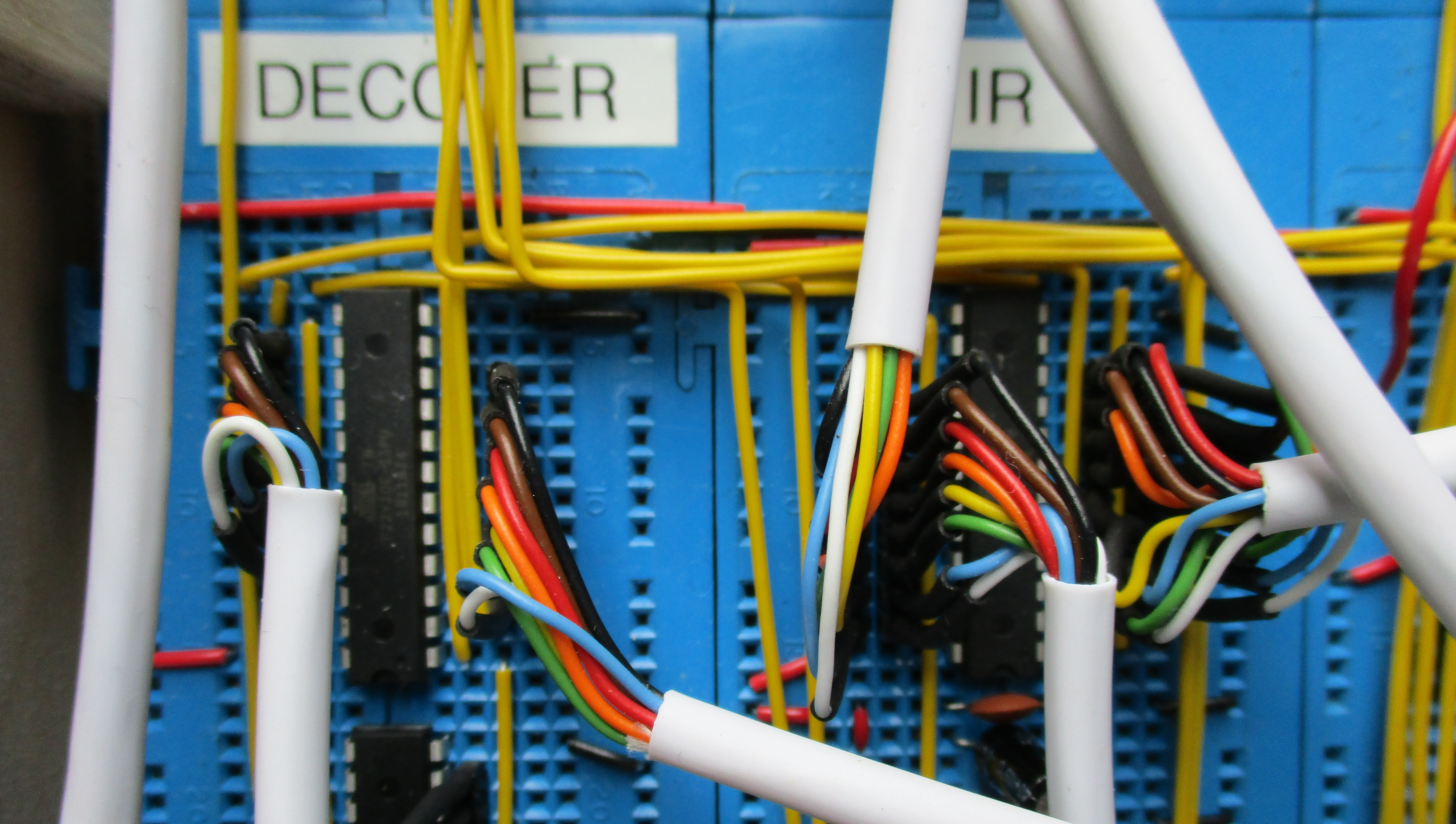
Figure 17 : Instruction register
Figure 18 : Instruction register circuit
The simpleCPU uses a 16 bit instruction format so we need two ATF22V10Cs to implement two 8bit registers i.e. to produce the required 16bit instruction register, as shown in figure 17. The IC on the left stores the high byte of the instruction, the IC on the right (mostly hidden under wires) stores the low byte of the instruction. The high byte contains the instruction opcode, the low byte the operand: 8bit immediate value, or 8bit absolute address. From a hardware point of view i could of used 7400 series logic to implement these two 8bit registers, but i decided to stick with the ATF22V10C from a stock / repair point of view i.e. one less IC to stock. As these are very simple registers i.e. just have a CE and CLR, the CUPL is equally simple as shown below:
Name     IR ;
PartNo   00 ;
Date     19/07/2019 ;
Revision 01 ;
Designer mike ;
Company  SimpleCPU ;
Assembly None ;
Location  ;
Device   g22v10 ;

Pin 1  = clk;      /*  system clock  */
Pin 2  = ce;       /*  clock enable  */

Pin 3  = D7;       /*  8bit input    */
Pin 4  = D6;
Pin 5  = D5;
Pin 6  = D4;
Pin 7  = D3;
Pin 8  = D2;
Pin 9  = D1;
Pin 10 = D0;

Pin 13 = clr;      /*  synchronous clear  */

/**  Outputs  **/

Pin 23 = Q7;       /*  8bit output  */
Pin 22 = Q6;
Pin 21 = Q5;
Pin 20 = Q4;
Pin 19 = Q3;
Pin 18 = Q2;
Pin 17 = Q1;
Pin 16 = Q0;

/** Fields **/

field Q = [Q7..0];
field D = [D7..0];

/** Equations **/

Q0.d = ((D0 & ce) # (Q0 & !ce)) & !clr;
Q1.d = ((D1 & ce) # (Q1 & !ce)) & !clr;
Q2.d = ((D2 & ce) # (Q2 & !ce)) & !clr;
Q3.d = ((D3 & ce) # (Q3 & !ce)) & !clr;
Q4.d = ((D4 & ce) # (Q4 & !ce)) & !clr;
Q5.d = ((D5 & ce) # (Q5 & !ce)) & !clr;
Q6.d = ((D6 & ce) # (Q6 & !ce)) & !clr;
Q7.d = ((D7 & ce) # (Q7 & !ce)) & !clr;
The code to implement these two 8bit registers in each SPLD is basically the same, but i did change the Q pin assignments for each IC to help with layout / wiring. Functionality is the same as the previous counter example in the initial SPLD section. The clock enable (CE) function is implemented as a multiplexer, selecting the current Q output or the new input. The Q outputs are updated on the rising edge of the system clock (CLK). Note, the registers are zeroed on power up by an internal circuit within the SPLD. The external clear line (CLR) is a synchronous clear i.e. this signal must be in a logic 1 state before the next clock rising edge to reset the outputs to a logic 0. The circuit diagram for the instruction register is shown in figure 18. Input data to the register comes from the data-out bus from the read only memory (ROM), storing the program. Output data from the register goes to the instruction decoder and arithmetic and logic unit (ALU).
Parts list for the instruction register circuit:
Figure 19 : Program counter
Figure 20 : Program counter circuit
The simpleCPU has an 8bit address bus, therefore, we need an 8bit loadable counter to implement the program counter. This just fits onto a single ATF22V10C, this device has enough flip-flops, but when you consider all the other required inputs it starts to get tight on pins. Again, the same multiplexer based clock enable circuit is used to hold the PC value between count updates. The program counter is normally incremented in the decode phase i.e. after an instruction has been fetched. The exception to this is when you are executing a JUMP instruction, here the fetched operand value is loaded into the program counter i.e. the absolute jump address. The address bus also needs to be updated to a different value when the processor is executing instructions that read/write to Random Access Memory (RAM). Switching the address bus between the PC value and the absolute address specified in an instruction (IR) could be performed using a multiplexer (as previously described), however, this would need a 25 pin device i.e. two ATF22V10C ICs, which would be most of a bread board. Therefore, to save space i used the tri-state outputs supported on these SPLD to implement a switched multiplexer. Here the data sources are switched on and off the shared address bus, the PC using the ATF22V10C and the absolute address using a 74HC245 octal bus transceiver (Link), as shown in figure 20. This type of multiplexer uses tri-state buffers to connect and disconnect different drivers onto and off a shared output. Unlike normal logic gates tri-state outputs can have three states: logic 0, logic 1 and disconnected. The truth table for the 74245 is given below:
The advantage of this type of implementation is that it significantly reduces pins and wiring counts, when compared to logic gate implemented multiplexer. The disadvantage is that it increases the time to switch between inputs. Consider the tri-state implementation below:
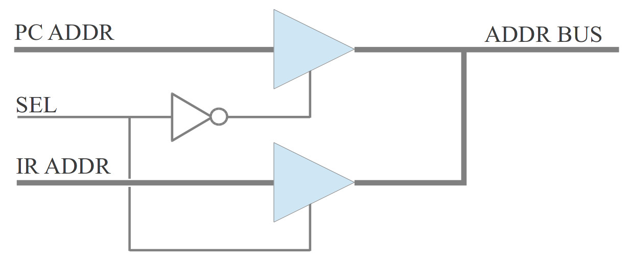
Figure 21 : Tri-state multiplexer
The two tri-state buffers are shown in blue, each having an 8bit input and output bus (thick line) and a single enable signal (thin line). To ensure that only one buffer is connected to the shared ADDR bus at any time a NOT gates is used i.e. if these tri-state buffers are enabled by a logic 1, the NOT gate ensures that only one enable line is high at any time. When SEL=0 ADDR=PC, when SEL=1 ADDR=IR. Unfortunately, this is not quite true, consider when SEL=0, this enables the top tri-state buffer, driving the PC value onto the ADDR bus. If the SEL line is changed to a logic 1 the top tri-state buffer will not see this until the NOT gate's output is updated, this will take a small amount of time i.e. the propagation delay of the NOT gate. The bottom tri-state buffer is driven directly by the SEL line, therefore, this buffer is updated almost immediately i.e. only wire/routing delays, driving the IR value onto the ADDR bus. As a result there is a small period of time where both tri-state buffers are enabled and therefore, may try to drive different logic values onto the same wire i.e. generate a short circuits. If you where doing this properly you would drive the enable lines separately, allowing some time for the tri-state buffers to switch to their disconnected state before enabling the next tri-state buffer, hence, slowing down their switching speeds. However, for this system i've gone for the cheap and dirty solution :). In this case the same control signal is used to control both the ATF22V10C and 74245. The 74245 output enable is active low, the ATF22V10C is active high.
The final CUPL source file for the PC is given below implementing a loadable 8bit counter with clock and output enable signals.
Name     PC ;
PartNo   00 ;
Date     19/07/2019 ;
Revision 01 ;
Designer mike ;
Company  SimpleCPU ;
Assembly None ;
Location UK ;
Device   g22v10;

/**************** INPUT PINS **********************/

PIN 1  = clk ; /* system clock                    */
PIN 2  = ce  ; /* clock enable      (active high) */
PIN 3  = ld  ; /* load counter      (active high) */

PIN 4  = D7  ; /* 8bit data in                    */
PIN 5  = D6  ; /*                                 */
PIN 6  = D5  ; /*                                 */
PIN 7  = D4  ; /*                                 */
PIN 8  = D3  ; /*                                 */
PIN 9  = D2  ; /*                                 */
PIN 10 = D1  ; /*                                 */
PIN 11 = D0  ; /*                                 */

PIN 13 = clr ; /* synchronous clear (active high) */
PIN 14 = oe  ; /* output enable     (active high) */

/**************** OUTPUT PINS *********************/

PIN 23 = Q0  ; /* 8bit count data out             */
PIN 22 = Q1  ; /*                                 */
PIN 21 = Q2  ; /*                                 */
PIN 20 = Q3  ; /*                                 */
PIN 19 = Q4  ; /*                                 */
PIN 18 = Q5  ; /*                                 */
PIN 17 = Q6  ; /*                                 */
PIN 16 = Q7  ; /*                                 */

/***************** EQUATIONS **********************/

Q0.d = (Q0 & !ce & !clr) # (!Q0 & !ld & ce) # (D0 & ld & ce);
Q1.d = (Q1 & !ce & !clr) # ((Q1 $ Q0) & !ld & ce) # (D1 & ld & ce);
Q2.d = (Q2 & !ce & !clr) # ((Q2 $ (Q1 & Q0)) & !ld & ce) # (D2 & ld & ce);
Q3.d = (Q3 & !ce & !clr) # ((Q3 $ (Q2 & Q1 & Q0)) & !ld & ce) # (D3 & ld & ce);
Q4.d = (Q4 & !ce & !clr) # ((Q4 $ (Q3 & Q2 & Q1 & Q0)) & !ld & ce) # (D4 & ld & ce);
Q5.d = (Q5 & !ce & !clr) # ((Q5 $ (Q4 & Q3 & Q2 & Q1 & Q0)) & !ld & ce) # (D5 & ld & ce);
Q6.d = (Q6 & !ce & !clr) # ((Q6 $ (Q5 & Q4 & Q3 & Q2 & Q1 & Q0)) & !ld & ce) # (D6 & ld & ce);
Q7.d = (Q7 & !ce & !clr) # ((Q7 $ (Q6 & Q5 & Q4 & Q3 & Q2 & Q1 & Q0)) & !ld & ce) # (D7 & ld & ce);

/***************** GLOBAL  ************************/

Q0.oe = oe;
Q1.oe = oe;
Q2.oe = oe;
Q3.oe = oe;
Q4.oe = oe;
Q5.oe = oe;
Q6.oe = oe;
Q7.oe = oe;
Parts list for the program counter circuit:
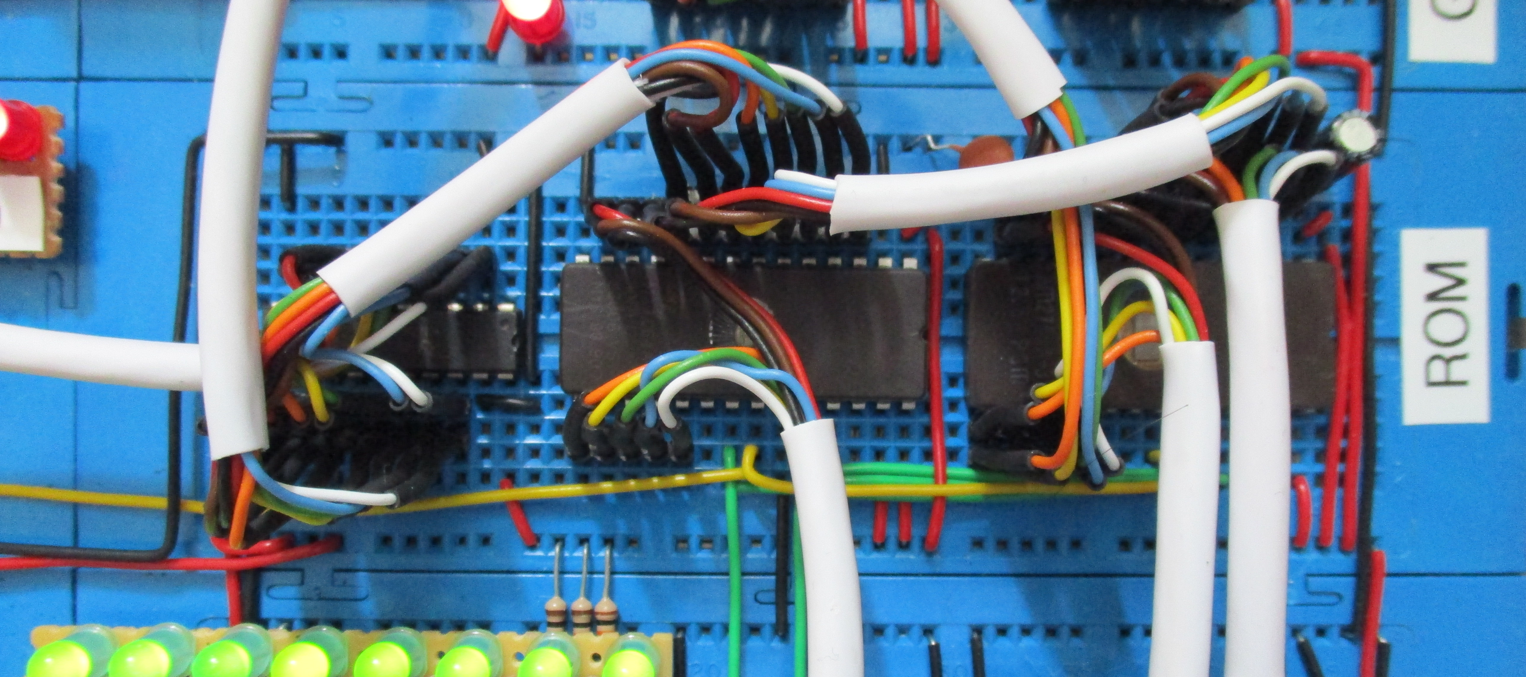
Figure 22 : Read Only Memory
The simpleCPU processor was initially based on a Von Neumann architecture (Link), i.e. a stored program computer, using one memory that contains both instructions and data, as shown in figure 23. However, when you move to implementation this raises the question (problem) of how do you load the user's program and data into memory? For most machines this requires a boot loader, a piece of software that loads the user's program into memory before it is executed, or non-volatile memory, memory that does not loose its data when the power is turned off. For a machine with only 256 memory locations i.e. an 8bit address bus, there isn't a lot of room for the boot loader and a user program to share. Therefore, you would normally divide the memory space into different regions: read only memory (ROM) i.e. memory that contains instructions and data that do not change, and random access memory (RAM) i.e. read/write memory, memory that the CPU can write data to and read back.
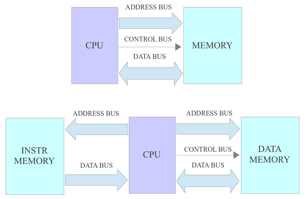
Figure 23 : Von Neumann (top) and Harvard (bottom) architectures
An alternative to the Von Neumann architecture is the Harvard architecture, here we have two memory blocks working in parallel, one containing instructions the other data i.e. instruction memory can not be used to store data, or vice versa. There are now two different address spaces i.e. you have address 0 in instruction memory and address 0 in data memory. Separate memory spaces in physically separate memory devices. This has the advantage that you can access instructions and data at the same time, allowing instruction overlap, but the main disadvantage is that you need two memory devices with their associated IO pins and Address, Data and Control buses. Which is a significant cost, therefore, the Von Neumann architecture was more common in early computers. However, with improvement in silicon technologies, the ever increasing available hardware and the drive to improve performance Harvard architectures now dominate.
When implementing the simpleCPU in an FPGA its was easier to base the design around a Von Neumann architecture as the FPGA supported dual port memories i.e. BlockRAM, giving me the separate uni-directional data-in and data-out buses, as shown in figure 2. Also this memory is easily to configure using the Xilinx software tools. For the SPLD implementation we do not have this luxury, as we will be using 2764 EPROMs (Link) for the instruction memory and 6264 RAM (Link) for data memory, the latter having a bi-directional data bus. Why did i select these memory devices? Simple, i had a big pile left over from an old module we used to teach: Chips to Systems. Note, the 2764 is windowed IC, if you expose this device to UV light you can erase its contents allowing it to be reprogrammed i.e. it is a non-volatile, Erasable Programmable Read-Only Memory (EPROM), ideal for storing the machine's program.
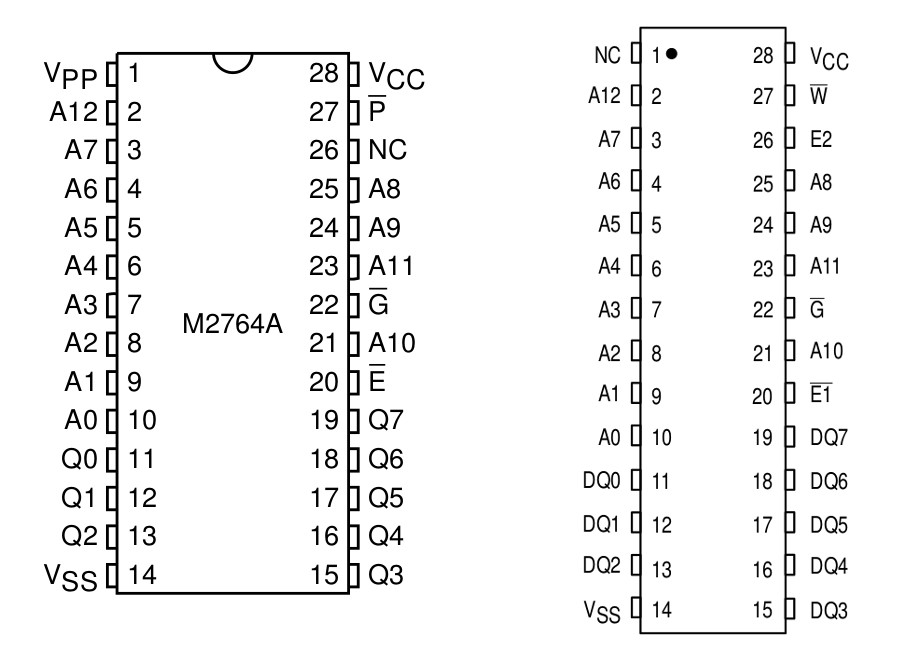
Figure 24 : ROM 2764 (left) and RAM 6264 (right)
These memory devices are quite old, commonly used in old Von Neumann computers from the 1980s. These processors typically used the same data bus (wires) to read and write data from and to memory (to reduce costs). When the CPU performs a read, memory drives data onto the data bus and when the CPU performs a write, the processor drives data onto the data bus. This requires tri-state bus drivers to be switch the CPU and memory on and off the shared data bus at different time as shown in figure 25. The Enable signal disconnects either the CPU or MEM output drivers from the data bus (wires), two drivers can not be connected to the same wire at the same time e.g. if one output's a logic 0 and one output's a logic 1, a short circuit will exist as you can't have different logic values on the same wire at the same time. As discussed in the previous multiplexer example tri-state designs tend to be slower than logic gate based ones, that's why they have been phased out of FPGA based designs (limited number of tri-state buffers in modern FPGAs).
Figure 25 : Bi-directional data bus
As we do not have dual port memory i.e. memory with separate data-in and data-out buses, and we only have an 8bit address buses i.e. can only address 256 memory locations, this raises the question: is there a better memory architecture for these new memory devices? The answer was Yes, a modified Harvard architecture. This version of the simpleCPU has two separate memory spaces: one for instructions and one for data i.e. again we can have two address 0s, one in instruction memory and one in data memory. However, unlike a normal Harvard architecture these memory devices share the same address and data buses i.e. these memories can not be accessed in parallel (not your normal definition of a modified Harvard). Therefore, we can now have 256 instructions and 256 data values. This is achieved by only enabling the 2764 ROM during an instruction fetch and only enabling the 6264 RAM during a LOAD or STORE instruction (instructions that read/write to variables in memory). Therefore, a small restriction on addressing modes e.g. you can not read data from ROM and you can not execute instructions from RAM, but as with designing any system, compromises are king.
Note, this is a key point when looking at different processor architectures, sometimes you look at a design and ask the questions: why did they do that? Normally the answer is that it made the hardware simpler to design or it was due to a hardware limitation i.e. we don't normally get to design the perfect solution, we work with what we have to hand.
The 2764 EPROM is a 8K x 8bit memory, as the address bus of the simpleCPU is only 8bits it can only address 256 locations. Therefore, to allow the memory to store multiple 256 instruction programs the higher address lines i.e. A8 - A10 are tied to DIP switches, as shown in figure 26. This allow up to 8 programs to be stored in this memory, address lines A11 and A12 are not used and tied to logic 0 i.e. we are only using 2048 bytes of the 8192 byte memory. Who needs more than eight program :). Note, as the processor only controls address lines A0 - A7, it does not see, or is aware of the higher address lines i.e. as far as the processor is concerned addresses 0x000, 0x100, 0x200, 0x300 etc are all address 0x00.
Figure 26 : ROM circuit
As the simpleCPU has an 16bit fixed length instruction format we need two 2764 EPROMS, one storing the high byte of the instruction i.e. the opcode, driving the high byte of the data bus. The other storing the low byte i.e. the operand, driving the low byte of the data bus. Both share the same address bus i.e. read the same location in each device. The only control signal used by the ROM is the OE pin, enabling the data bus during the instruction fetch phase (controlled by the decoder discussed later). Parts list for the Read Only Memory circuit:
Figure 27 : Random Access Memory
As discussed in the previous section the simpleCPU uses a 6264 RAM component. As the CPU's address bus is only 8bits, address lines A8 - A12 are tied to logic 0 i.e. we are only using 256 bytes of the 8192 byte memory. This is slightly on the wasteful side. If needed we could expand the amount of memory accessible to the CPU by implementing an expanded memory model (Link) by implementing a 256 byte bank switching scheme, but as this system is only running simple demonstration programs there was no real need for a system with more RAM. To be honest i'm only using a handful of memory locations for temporary storage, so 256 was a lot more than i needed. A bigger ROM would be more usesful i.e. programs with more than 256 instructions (its surprising how quickly you run out of space), but this would require modifications to the instruction format and the hardware, and as previously discussed the PC only just fits into one ATF22V10C so this would be a lot of work for no real identified need. The final RAM circuit diagram is shown in figure 28.

Figure 28 : Random Access Memory circuit
Data input to the memory i.e. DI0 - DI7 is the data output from the the CPU i.e. the output of the accumulator (ACC), the single general purpose data register in the CPU. During a STORE instruction this data needs to be driven onto the RAM's data bus, therefore, as previously discussed we need another 74HC245 octal bus transceiver i.e. we can not drive the output of the ACC onto the shared data bus whilst we are fetching an instruction etc. The RAM component has two control lines: output enable (G) and write enable (WR). These signals and the 74245 output enable (DATA_OE) are controlled by the decoder logic described later.
Parts list for the Random Access Memory circuit:
Figure 29 : Arithmetic and Logic Unit
The ALU was the most complicated element of this implementation, very tricky to get all the required functionality into the ATF22V10C ICs. However, there was quite a bit of design flexibility in how the control signals were encoded and how this affected the ALU's internal structure e.g. one-hot or binary encoded etc. After a bit of trial and error i went for a 3bit (octal) bit sliced design. Bit slicing (Link) dates back to the early days of third generation computing, where functional block were implemented by chaining together a standard module/IC. This simplified IC development as you could design and build an IC with a smaller bit width e.g. a 4bit bit sliced adder, then by connecting three of these ICs together you could create a 12bit adder. Ive taken the same approach here, this version of the simpleCPU is an accumulator (ACC) based architecture i.e. has one general purpose registers, therefore, each ATF22V10C implements a 3bit ALU combined with a 3bit accumulator (ACC). A block diagram representation of this design is shown in figure 30, the ALU performs the following functions:
where YA=IR(7:0), YB=MEM_DO(7:0), Z=ACC(7:0)
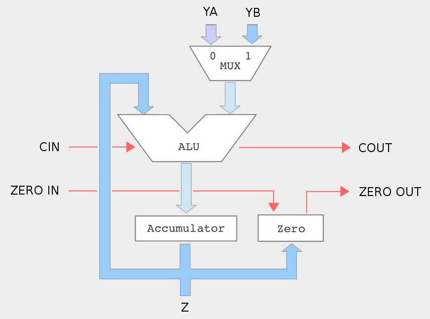
Figure 30 : 3bit sliced ALU + ACC + MUX block diagram
This design is replicated three times to produce a 9bit ALU/ACC, of which only the lower 8bits are used. When chaining these modules together the COUT and ZERO_OUT of the lower digit slice drive the CIN and ZERO_IN of the next. Note, this module implements the heart of the CPU, when compared back to figure 2 you can see that quite a lot of the processor is contained in these three ICs. The CUPL representation of this hardware is shown below:
Name     alu ;
PartNo   00 ;
Date     21/07/2019 ;
Revision 01 ;
Designer mike ;
Company  SimpleCPU ;
Assembly None ;
Location  ;
Device   g22v10;

/** Inputs **/

Pin 1 = CLK;      /*   system clock    */
Pin 2 = CE;       /*   clock enable    */
Pin 3 = ZIN;      /*   zero detect in from previous slice   */

Pin 4 = YA2;      /*   3bit input YA   */
Pin 5 = YA1;
Pin 6 = YA0;
Pin 7 = YB2;      /*   3bit input YB   */
Pin 8 = YB1;
Pin 9 = YB0;

Pin 10 = CTL1;    /*   control inputs CTL0 & CTL1   */
Pin 11 = CTL0;

/** Outputs **/

Pin 23 = ZOUT;    /*   zero detect out   */

Pin 22 = C2;      /*   carry outs from adder   */
Pin 21 = C1;
Pin 20 = C0;

Pin 19 = Z2;      /*   3bit  ACC output
Pin 18 = Z1;
Pin 17 = Z0;

Pin 15 = CTL2;    /*   control input CTL2    */
Pin 14 = CIN;     /*   carry in from previous slice    */
Pin 13 = CLR;     /*   synchronous clear    */


/* ALU */

/* CTL 2  CTL1  CTL0         */
/* 0      X     0    ADD     */
/* 0      X     1    SUB     */
/* 1      0     0    PASS YA */
/* 1      0     1    PASS YB */
/* 1      1     0    AND     */

/* DATA */

/* YA = IMMEDIATE FROM IR
/* YB = DATA FROM RAM */

/* ZER0 FLAG */
ZOUT = (Z2 # Z1 # Z0 # ZIN);

/* INVERT YA */
T0 = ((YA0 & !CTL0) # (!YA0 & CTL0)) ;
T1 = ((YA1 & !CTL0) # (!YA1 & CTL0)) ;
T2 = ((YA2 & !CTL0) # (!YA2 & CTL0)) ;

/* ADDER / MUX */
Z0.d = (Z0 & !CE & !CLR) # ( ((Z0 $ CIN $ T0) & !CTL2) # ((YA0 & !CTL1 & !CTL0) # (YB0 & !CTL1 & CTL0) # (Z0 & YA0 & CTL1 & !CTL0)) & CTL2 ) & CE;
C0   = ((Z0 & T0) # (Z0 & CIN) # (T0 & CIN)) ;

Z1.d = (Z1 & !CE & !CLR) # ( ((Z1 $ C0 $ T1) & !CTL2)  # ((YA1 & !CTL1 & !CTL0) # (YB1 & !CTL1 & CTL0) # (Z1 & YA1 & CTL1 & !CTL0)) & CTL2 ) & CE;
C1   = ((Z1 & T1) # (Z1 & C0) # (T1 & C0)) ;

Z2.d = (Z2 & !CE & !CLR) # ( ((Z2 $ C1 $ T2) & !CTL2)  # ((YA2 & !CTL1 & !CTL0) # (YB2 & !CTL1 & CTL0) # (Z2 & YA2 & CTL1 & !CTL0)) & CTL2 ) & CE;
C2   = ((Z2 & T2) # (Z2 & C1) # (T2 & C1)) ;
This ALU is based on the original simpleCPU v1 design as previously described here: (Link), refer back to this for more info. The ALU component has three control lines: CTL0, CTL1 and CTL2. These signals are controlled by the decoder logic described later. Also used by this control logic is the final ZERO_OUT, used in conditional JUMPs. Note, i did think of using the COUT for conditional carry JUMPs, but this adds a few "problems" when you consider the 2's complimented subtraction used in the ALU i.e. what does the carry bit indicate? Also the decoder hardware was getting a bit tight on space so decided to skip this for now. The circuit diagram for this ALU is shown in figure 31.
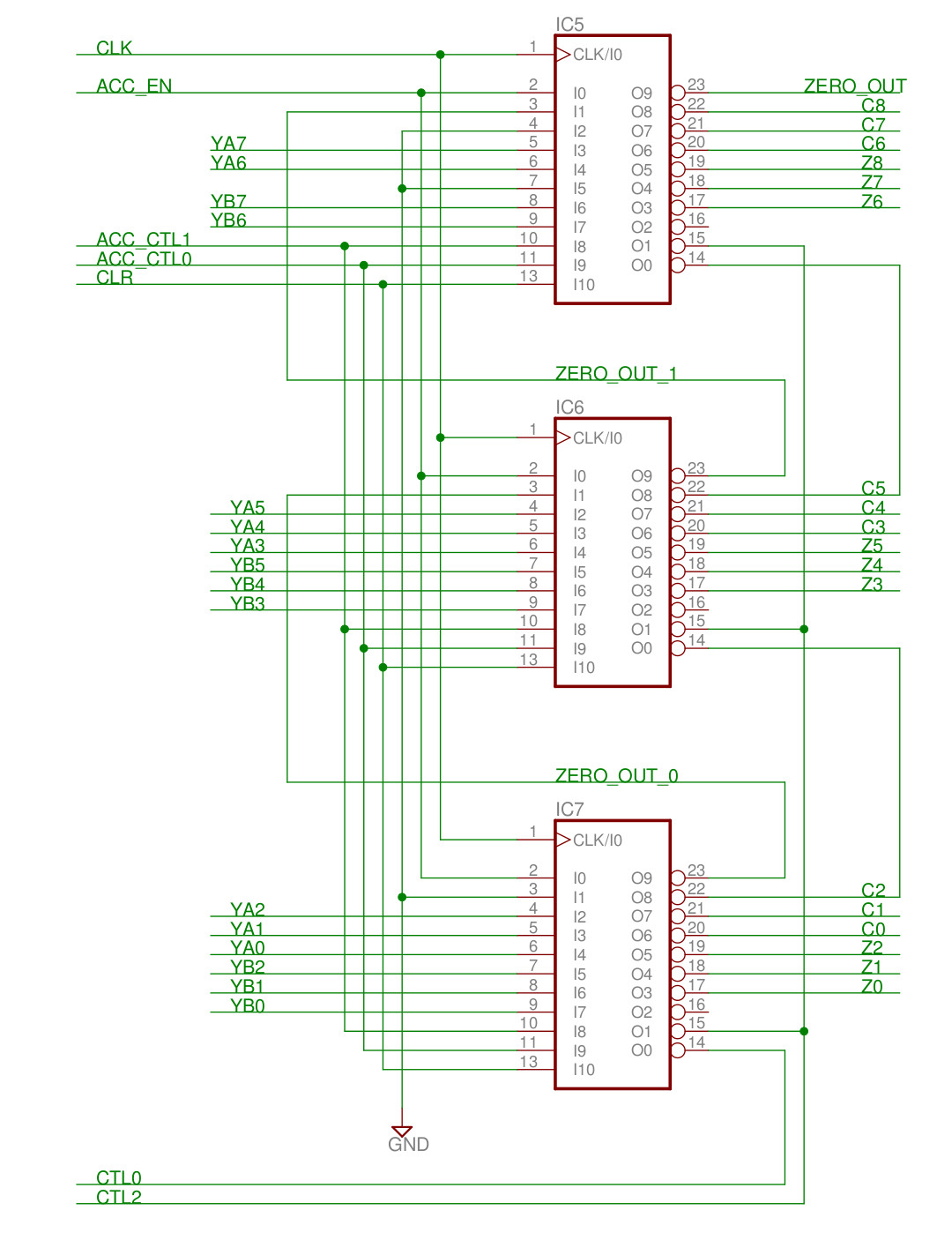
Figure 31 : 3bit sliced ALU + ACC + MUX circuit diagram
Parts list for the Arithmetic and Logic Unit circuit:

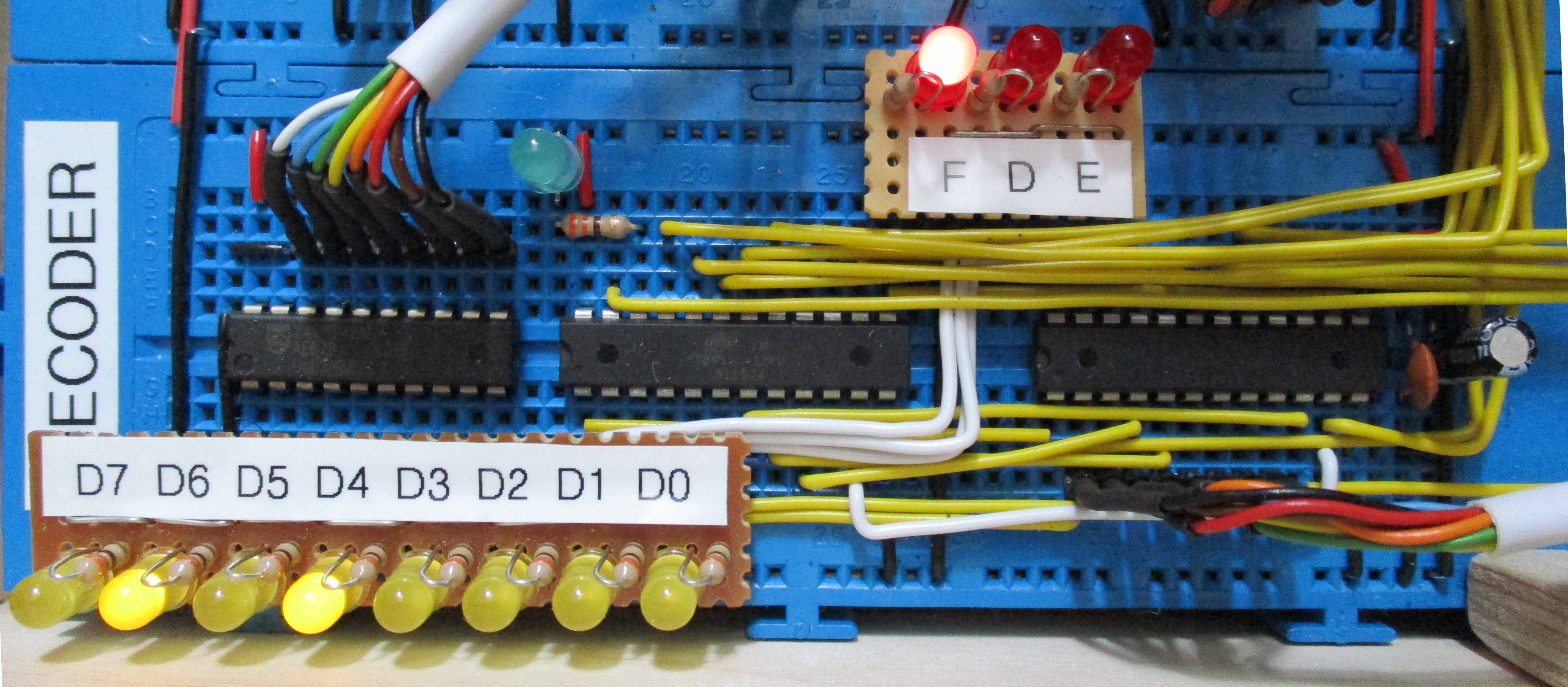
Figure : 32 Control logic
The "brains" of the CPU, decoding instructions and controlling all of the previously described sub-systems. When processing an instruction the first thing the CPU needs to know is what phase of the instruction is currently being performed i.e. fetch, decode or execute. In the CPU this is represented using a simple 3bit ring counter (Link), representing the processor's state as a one-hot value. This ring counter requires three flip-flops to hold the 3bit one-hot value, we could reduce the number of flip-flops down to 2 if we switched to binary encoding, however, this would require more complex decoding logic to determine the processor's state i.e. you would need to decode two bits to determine its value, were as using one-hot you only need to look at one bit, as there is only ever one logic 1 at any one time.
There are a lot of different ways to design the hardwired control logic used in the decoder. The method used in this design does not produce a minimal solution i.e. in terms of logic gates, but from a teaching view point does break the design process down into what i hope are more easily understood steps:
From the previously discussed sub-systems the CPU has the following control signals:
These are used to implement the following register transfer level (RTL) description of each instruction:
Note, in RTL syntax "<-" reads as "updated with", M[X] is memory, addressed at location X.
STEP1: the state of each signal can be defined for each instruction during each phase:
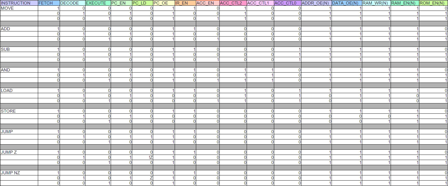
Figure : 33 Control signals
STEP2: each instruction is assigned an unique 4bit opcode, which is stored in the top nibble of each instruction, these can be converted into a one-hot representation using the following logic. Again, the reason for converting the 4bit binary representation into a one-hot representation is that it simplifies the later decoding logic i.e. to identify the current fetched instruction you only need to look at one bit. Note, this one-hot encoded signal is used to drive an LED array, so that the user can easily see what instruction is being executed i.e. only one LED is ever illuminated.
Note, had a slight rephrasing of instruction names to match version-3 simpleCPU assembler syntax. Rather than using INPUT and OUTPUT as the instruction names used to refer to reading and writing to memory, i have reverted back to LOAD and STORE as these instruction names are more common (widely used in RISC type processors). I found that using the word LOAD for the instruction that moves data into a register caused a bit of confusion for some students who have used the more typical interpretation of the word LOAD. Also, apologies i'm not sure i'm consistent with opcode values i.e. that machine code may not be the same as the other version of this processor, sorry :(, but code portability wasn't a high priority (i forgot to check), getting it to fit in the SPLDs was the goal.
INSTR   IR15 IR14 IR13 IR12 IR11 IR10 IR09 IR08
MOVE    0    0    0    0    X    X    X    X
ADD     0    0    0    1    X    X    X    X
SUB     0    0    1    0    X    X    X    X
AND     0    0    1    1    X    X    X    X
LOAD    0    1    0    0    X    X    X    X
STORE   0    1    0    1    X    X    X    X
JUMPU   1    0    0    0    X    X    X    X
JUMPZ   1    0    0    1    X    X    X    X
JUMPNZ  1    0    1    0    X    X    X    X

move   = NOT IR15 AND NOT IR14 AND NOT IR13 AND NOT IR12
add    = NOT IR15 AND NOT IR14 AND NOT IR13 AND     IR12
sub    = NOT IR15 AND NOT IR14 AND     IR13 AND NOT IR12
and    = NOT IR15 AND NOT IR14 AND     IR13 AND     IR12
load   = NOT IR15 AND     IR14 AND NOT IR13 AND NOT IR12
store  = NOT IR15 AND     IR14 AND NOT IR13 AND     IR12
jumpU  =     IR15 AND NOT IR14 AND NOT IR13 AND NOT IR12
jumpZ  =     IR15 AND NOT IR14 AND NOT IR13 AND     IR12
jumpNZ =     IR15 AND NOT IR14 AND     IR13 AND NOT IR12
STEP3: using simple intuitive logic circuits the one-hot state and opcode representations can be combined to produce the required control signals:
ir_en      = fetch
rom_en     = NOT fetch

ram_en     = NOT( (decode OR execute) AND load)
ram_wr     = NOT( decode AND store )

addr_oe    = NOT( (decode OR execute) AND (load OR store) )
data_oe    = NOT( decode AND store )

pc_en    = (decode AND NOT(jumpU OR (jumpZ AND NOT zero) OR (jumpNZ AND zero)) ) OR (execute AND (jumpU OR (jumpZ AND NOT zero) OR (jumpNZ AND zero)) )
pc_ld    = ( jumpU OR (jumpZ AND NOT zero) OR (jumpNZ AND zero) )
pc_oe    = NOT( (decode OR execute) AND (load OR store) )

CTL2  CTL1  CTL0
0     X     0     ADD
0     X     1     SUB
1     0     0     PASS YA
1     0     1     PASS YB
1     1     0     AND

acc_ctl2 = move OR load OR and
acc_ctl1 = and
acc_ctl0 = sub OR load

acc_en   = (move OR add OR sub OR and OR load) AND execute
This functionality is spread over three ATF22V10C, mainly due to the lack of pins rather than the complexity of the logic. The CUPL source file for each decoder chip is given below:
Name     Decoder0;
PartNo   00 ;
Date     20/07/2019 ;
Revision 01 ;
Designer mike ;
Company  SimpleCPU ;
Assembly None ;
Location  ;
Device   g22v10;

/* *************** INPUT PINS ******************** */

PIN 1  = clk;      /*   system clock               */
PIN 4  = IR15;     /*   high byte of IR            */
PIN 5  = IR14;     /*                              */
PIN 6  = IR13;     /*                              */
PIN 7  = IR12;     /*                              */
PIN 8  = IR11;     /*                              */
PIN 9  = IR10;     /*                              */
PIN 10 = IR09;     /*                              */
PIN 11 = IR08;     /*                              */
PIN 13 = clr;      /*   synchronous clear          */

/* *************** OUTPUT PINS ******************* */

PIN 23 = move;      /*   one-hot decoded outputs   */
PIN 22 = add;       /*                             */
PIN 21 = sub;       /*                             */
PIN 20 = and;       /*                             */
PIN 19 = load;      /*                             */
PIN 18 = store;     /*                             */
PIN 17 = jumpU;     /*                             */
PIN 16 = jumpZ;     /*                             */
PIN 15 = jumpNZ;    /*                             */
PIN 14 = jumpNZbuf; /*                             */

/* INSTR   IR15 IR14 IR13 IR12 IR11 IR10 IR09 IR08 */
/* MOVE    0    0    0    0    X    X    X    X    */
/* ADD     0    0    0    1    X    X    X    X    */
/* SUB     0    0    1    0    X    X    X    X    */
/* AND     0    0    1    1    X    X    X    X    */
/* LOAD    0    1    0    0    X    X    X    X    */
/* STORE   0    1    0    1    X    X    X    X    */
/* JUMPU   1    0    0    0    X    X    X    X    */
/* JUMPZ   1    0    0    1    X    X    X    X    */
/* JUMPNZ  1    0    1    0    X    X    X    X    */

move   = (!IR15 & !IR14 & !IR13 & !IR12);
add    = (!IR15 & !IR14 & !IR13 & IR12);
sub    = (!IR15 & !IR14 & IR13  & !IR12);
and    = (!IR15 & !IR14 & IR13  & IR12);
load   = (!IR15 & IR14  & !IR13 & !IR12);
store  = (!IR15 & IR14  & !IR13 & IR12);
jumpU  = (IR15  & !IR14 & !IR13 & !IR12);
jumpZ  = (IR15  & !IR14 & !IR13 & IR12);
jumpNZ = (IR15  & !IR14 & IR13  & !IR12);
The outputs from this conversion are used to drive the next two decoder ICs (decoder1 and decoder2) and an LED array, as shown in figure 34. This array displays the decoded one-hot value so that the user can quickly identify what of the nine instructions is to be executed. As the decoder is driven from the IR this will only update at the end of the fetch phase i.e. during the decode.

Figure : 34 Decoded LED array
Name     Decoder1 ;
PartNo   00 ;
Date     20/07/2019 ;
Revision 01 ;
Designer mike ;
Company  SimpleCPU ;
Assembly None ;
Location  ;
Device   g22v10;

/* *************** INPUT PINS *********************/

PIN 1  = clk;      /*   system clock              */
PIN 2  = jumpZ;    /*   one-hot decoded inputs    */
PIN 3  = jumpU;    /*                             */
PIN 4  = store;    /*                             */
PIN 5  = load;     /*                             */
PIN 6  = and;      /*                             */
PIN 7  = sub;      /*                             */
PIN 8  = add;      /*                             */
PIN 9  = move;     /*                             */
PIN 10 = jumpNZ;   /*                             */
PIN 11 = zero;     /*   zero in                   */
PIN 13 = clr;      /*   synchronous clear         */

/* *************** OUTPUT PINS ********************/

PIN 23 = fetch;    /*  3bit ring counter          */
PIN 22 = decode;   /*                             */
PIN 21 = execute;  /*                             */
PIN 20 = pc_en;    /*  PC control signals         */
PIN 19 = pc_ld;    /*                             */
PIN 18 = pc_oe;    /*                             */
PIN 17 = acc_ctl2; /*  ALU control signals        */
PIN 16 = acc_ctl1; /*                             */
PIN 15 = acc_ctl0; /*                             */
PIN 14 = acc_en;   /*                             */

fetch.d = execute # clr;
decode.d = fetch & !clr;
execute.d = decode & !clr;

T0 =  (jumpU # (jumpZ & !zero) # (jumpNZ & zero));        /*  shared logic */

pc_en    = (decode & !T0) # (execute & T0);               /*  PC           */
pc_ld    = T0;                                            /*               */
pc_oe    = !((decode # execute) & (load # store));        /*               */

/* CTL 2  CTL1  CTL0         */
/* 0      X     0    ADD     */
/* 0      X     1    SUB     */
/* 1      0     0    PASS YA */
/* 1      0     1    PASS YB */
/* 1      1     0    AND     */

acc_ctl2 = move # load # and;                             /*  ALU          */
acc_ctl1 = and;                                           /*               */
acc_ctl0 = sub # load;                                    /*               */

acc_en   = (move # add # sub # and # load) & execute;     /*  ACC CE       */
The one-hot fetch, decode and execute control signals are also passed to the final decode IC (decode2) and a LED array, as shown in figure 35. These signal being buffered by additional drivers in the decoder1 IC. A short video of the clock showing the relationship between the clock and the fetch, decode and execute phases available here: (Video). You may think this video does not show much, but its aim is to demonstrate that each instruction requires three clock cycles to complete i.e. on each clock pulse the ring counter is 'incremented', moving the one-hot token to the next position, after three clock cycles the token is back the start, triggering the fetch of the next instruction. A key element that determines the speed of a processor is its Clock Cycles per Instruction (CPI), the lower this value the more instructions executed per second, therefore, more processing performance (well in theory).
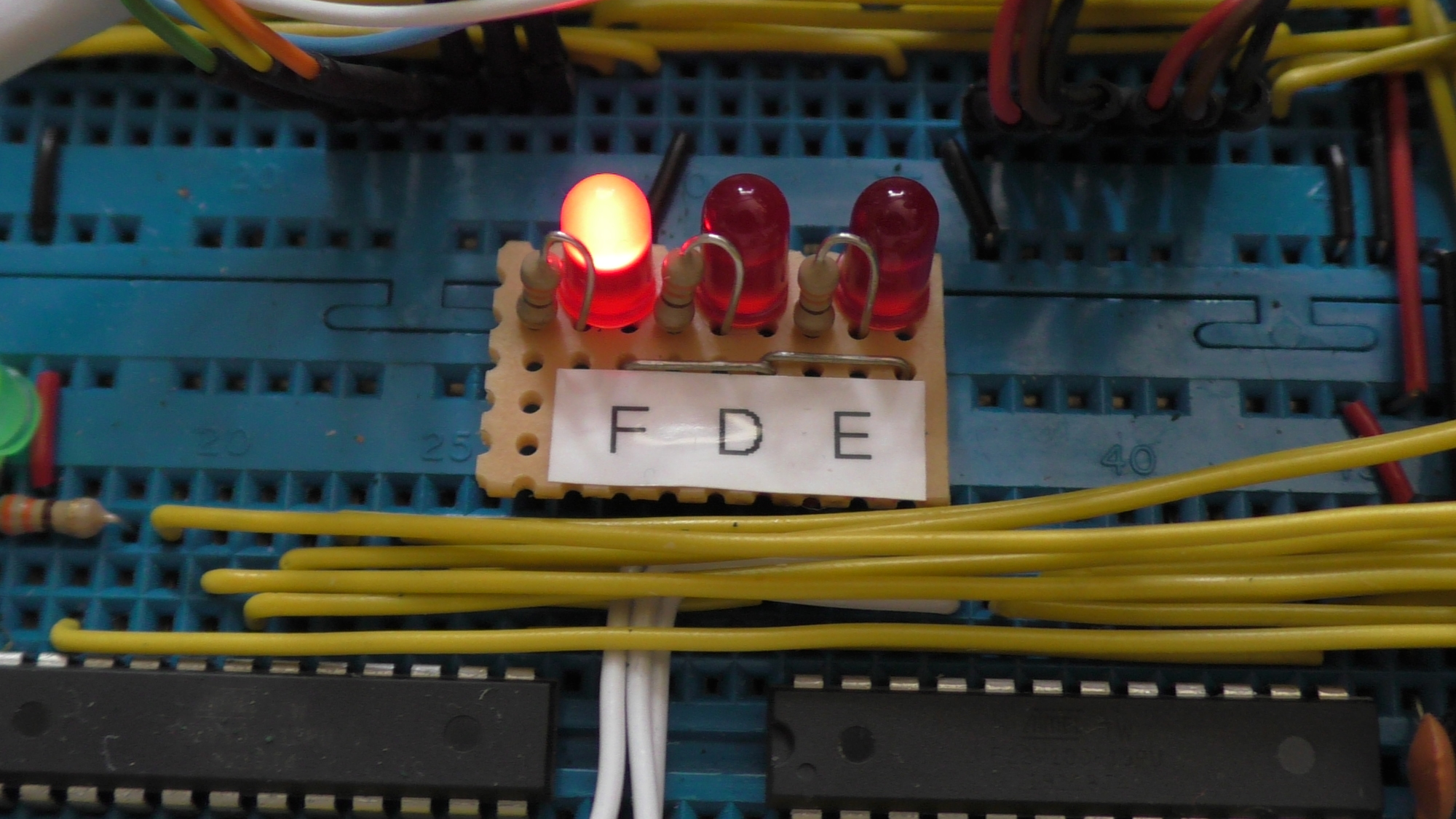
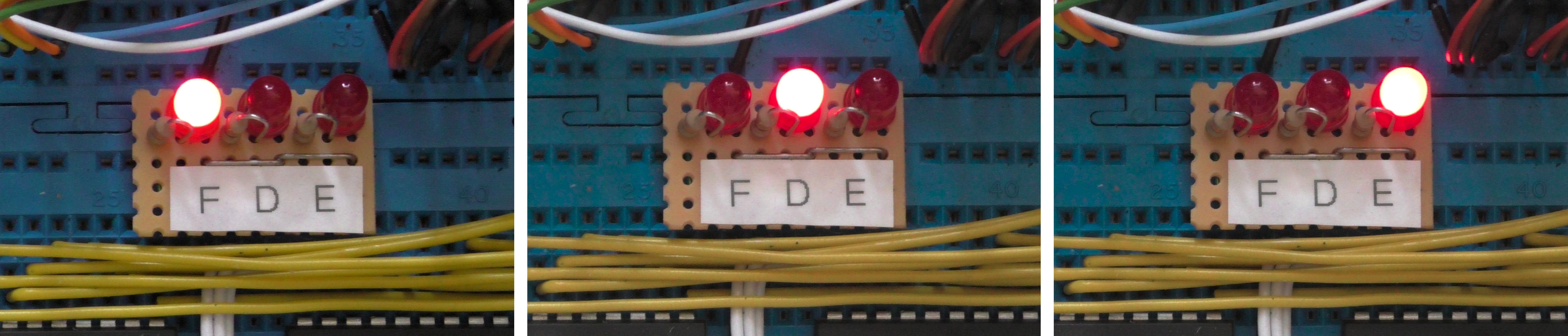
Figure : 35 FDE LED array
Name     Decoder2 ;
PartNo   00 ;
Date     20/07/2019 ;
Revision 01 ;
Designer mike ;
Company  SimpleCPU ;
Assembly None ;
Location  ;
Device   g22v10;

/* *************** INPUT PINS *********************/

PIN 1  = clk;     /*    system clock             */
PIN 2  = fetch;   /*    3bit state inputs        */
PIN 3  = decode;  /*                             */
PIN 4  = execute; /*                             */
PIN 5  = jumpU;   /*    one-hot decoded inputs   */
PIN 6  = jumpZ;   /*                             */
PIN 7  = jumpNZ;  /*                             */
PIN 8  = load;    /*                             */
PIN 9  = store;   /*                             */
PIN 11 = zero;    /*                             */
PIN 13 = clr;     /*    synchronous clear        */

/* ************** OUTPUT PINS ********************/

PIN 23 = ir_en;       /*   IR control signal     */
PIN 22 = zeroBuf;     /*   zero bit LED          */
PIN 21 = rom_en;      /*   ROM output enable     */
PIN 20 = addr_oe;     /*   ADDR output enable    */
PIN 19 = data_oe;     /*   DATA output enable    */
PIN 18 = ram_en;      /*   RAM output enable     */
PIN 17 = ram_wr;      /*   RAM write enable      */
PIN 16 = fetchBuf;    /*   LED buffers           */
PIN 15 = decodeBuf;   /*                         */
PIN 14 = executeBuf;  /*                         */

zeroBuf    = zero;
fetchBuf   = fetch;
decodeBuf  = decode;
executeBuf = execute;

ir_en      = fetch;
rom_en     = !fetch;

ram_en     = !((decode # execute) & load);
ram_wr     = !(decode & store);

addr_oe    = !((decode # execute) & (load # store));
data_oe    = !(decode & store);
The circuit diagram for the control logic is shown in figure 36.
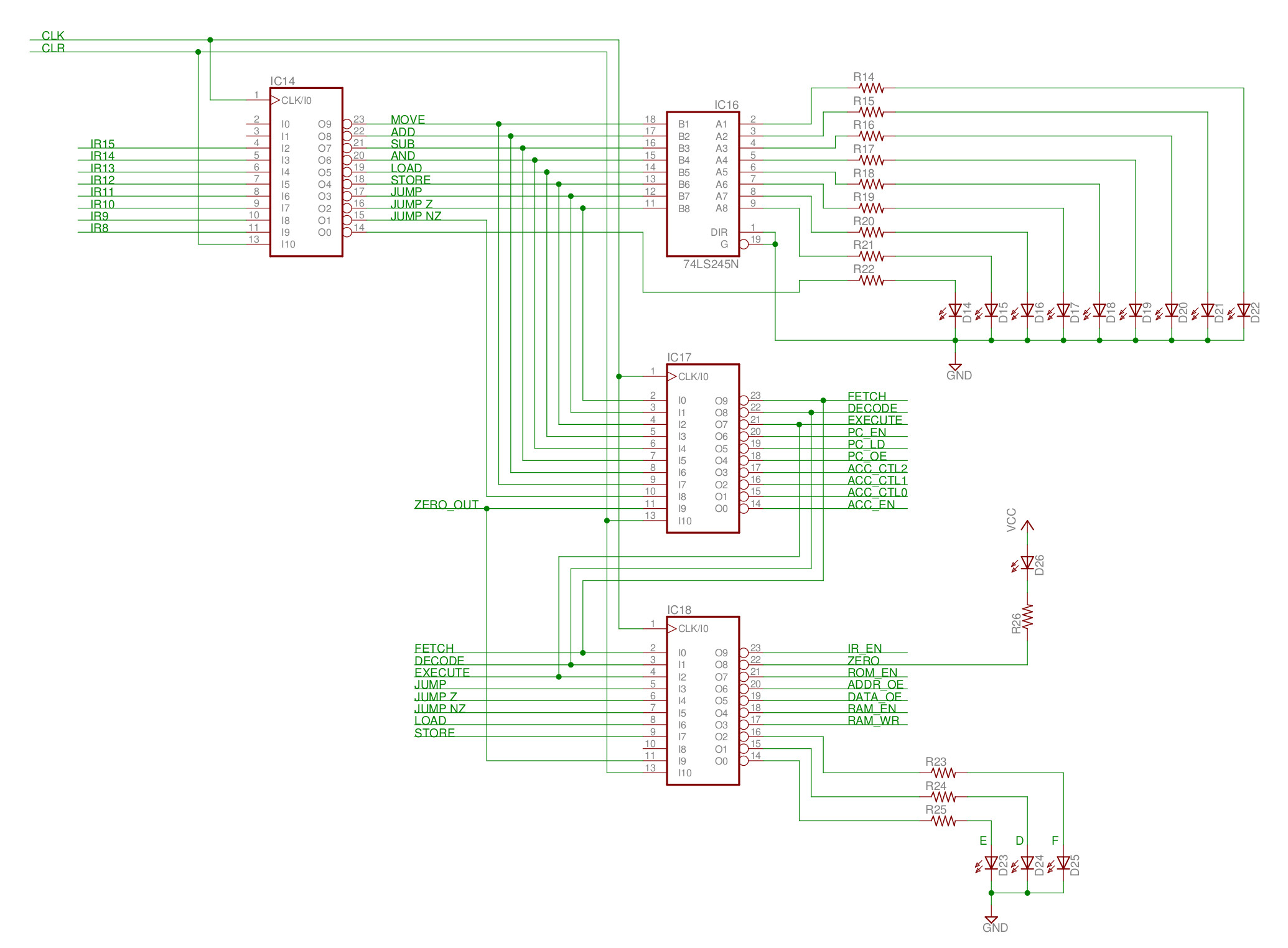
Figure : 36 Control logic circuit
Parts list for the Control Logic circuit: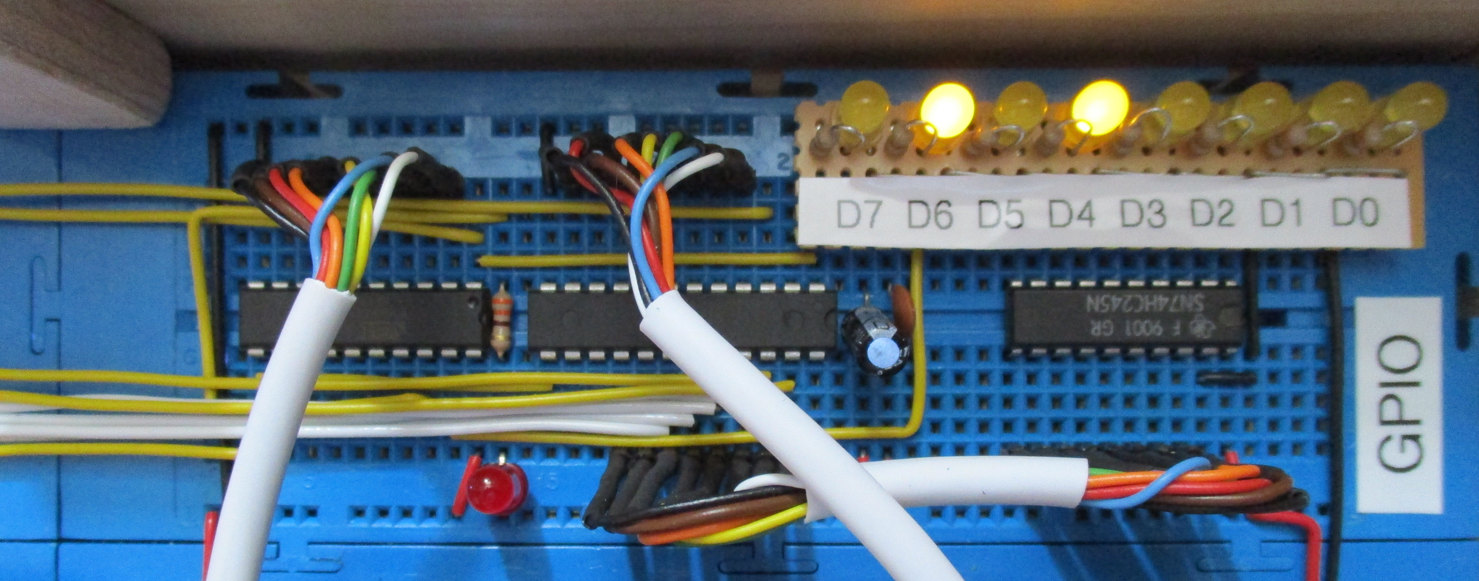
Figure : General Purpose Input/Output
A computer with no outputs is a heater :). Therefore, i needed to make this computer do something, and with any computer the first program you should always write is "Hello World". To this end i added a 16x2 LCD display. To control this display you need at least 6bits of parallel IO i.e. some GPIO, well more of a GPO, general purpose outputs. For this LCD you don't need any inputs to display characters. Note, inputs are sometimes needed for handshakes in data transfers i.e. to synchronise the transmitting (TX) and receiving (RX) hardware. To interface to this parallel port some processors have special INPUT / OUTPUT instructions, specifically designed to work with GPIO. However, like many processors the simpleCPU does not support these types of instructions (to save space), therefore, these interface devices are memory mapped i.e. assigned an external memory address. Now, when the processor writes to this specific memory address the data it writes will be used to update/drive these IO (output) pins. Typically, when the processor writes to this assigned address all other memory devices attached to the shared bus are disabled. However, ive taken a slightly different approach. When you read an output port (GPO) the processor can not read back the data it has written, as the outputs of the output port are connected to external pins, rather than driving the data bus (as would be the case for RAM). Therefore, to allow the processor to keep a record of what data it has been written to the output port (without adding more hardware), a write to the assigned address writes data to both the GPO and RAM. When the processor reads the assigned memory address it will only read RAM as the GPO is not connected to the data-in bus of the CPU. This adds additional functionality and reduces hardware, so a win, win. To keep the GPO out of the way of other data/variables i assigned it the address 0xFF i.e. the last address in data memory.
The hardware needed to implement this output port is very simple, comparable to the other registers we have looked at. The address decoder i.e. the logic that determines if the processor is writing to the output port is a nine input AND gate. When the processor executes the instruction STORE 0xFF, the data in the ACC will be placed on the data bus, the address bus will be set to 0xFF enabling the output port (and RAM), as shown in the circuit diagram in figure 37.
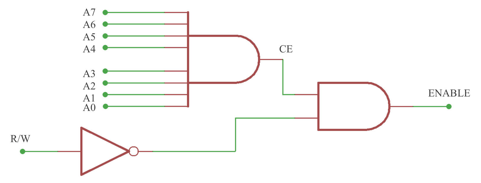
Figure : 37 Address decoder circuit
where RAM_WR=R/W, ADDRESS_BUS=A7:A0, GPO_CE=ENABLE. The CUPL source files for the GPO port and address decoder are shown below:
Name     Address_Decoder;
PartNo   00 ;
Date     20/07/2019 ;
Revision 01 ;
Designer mike ;
Company  SimpleCPU ;
Assembly None ;
Location  ;
Device   g16v8;

/* *************** INPUT PINS *********************/

PIN 1  = CLK;      /*  system clock               */
PIN 2  = A7;       /*  8bit address bus           */
PIN 3  = A6;       /*                             */
PIN 4  = A5;       /*                             */
PIN 5  = A4;       /*                             */
PIN 6  = A3;       /*                             */
PIN 7  = A2;       /*                             */
PIN 8  = A1;       /*                             */
PIN 9  = A0;       /*                             */

/* *************** OUTPUT PINS ********************/

PIN 19 = GPIO;     /*  GPO enable                 */
PIN 18 = LED;      /*  GPO enable LED             */
PIN 11 = CLR;      /*  synchronous clear          */

GPIO  =  (A7 & A6 & A5 & A4 & A3 & A3 & A1 & A0 & !CLR);
LED   = !(A7 & A6 & A5 & A4 & A3 & A3 & A1 & A0 & !CLR);
Name     GPIO ;
PartNo   00 ;
Date     19/07/2019 ;
Revision 01 ;
Designer mike ;
Company  SimpleCPU ;
Assembly None ;
Location  ;
Device   g22v10 ;

/* *************** INPUT PINS *********************/

Pin 1  = clk;      /*  system clock               */
Pin 2  = en;       /*  clock enable               */
Pin 3  = wr;       /*  write enable               */

Pin 4  = D7;       /*  8bit data input            */
Pin 5  = D6;
Pin 6  = D5;
Pin 7  = D4;
Pin 8  = D3;
Pin 9  = D2;
Pin 10 = D1;
Pin 11 = D0;

Pin 13 = clr;      /*  synchronous cleat          */

/* *************** OUTPUT PINS ********************/

Pin 23 = Q7;    /* E  */
Pin 22 = Q6;    /* RS */
Pin 21 = Q5;    /* D7 */
Pin 20 = Q4;    /* D6 */
Pin 19 = Q3;    /* D5 */
Pin 18 = Q2;    /* D4 */
Pin 17 = Q1;    /* NU */
Pin 16 = Q0;    /* NU */

/* ***************** FIELDS  **********************/

field Q = [Q7..0];
field D = [D7..0];

/* **************** EQUATIONS *********************/

ce = en & !wr;

Q0.d = ((D0 & ce) # (Q0 & !ce)) & !clr;
Q1.d = ((D1 & ce) # (Q1 & !ce)) & !clr;
Q2.d = ((D2 & ce) # (Q2 & !ce)) & !clr;
Q3.d = ((D3 & ce) # (Q3 & !ce)) & !clr;
Q4.d = ((D4 & ce) # (Q4 & !ce)) & !clr;
Q5.d = ((D5 & ce) # (Q5 & !ce)) & !clr;
Q6.d = ((D6 & ce) # (Q6 & !ce)) & !clr;
Q7.d = ((D7 & ce) # (Q7 & !ce)) & !clr;
The circuit diagram for the General Purpose Output is shown in figure 38.
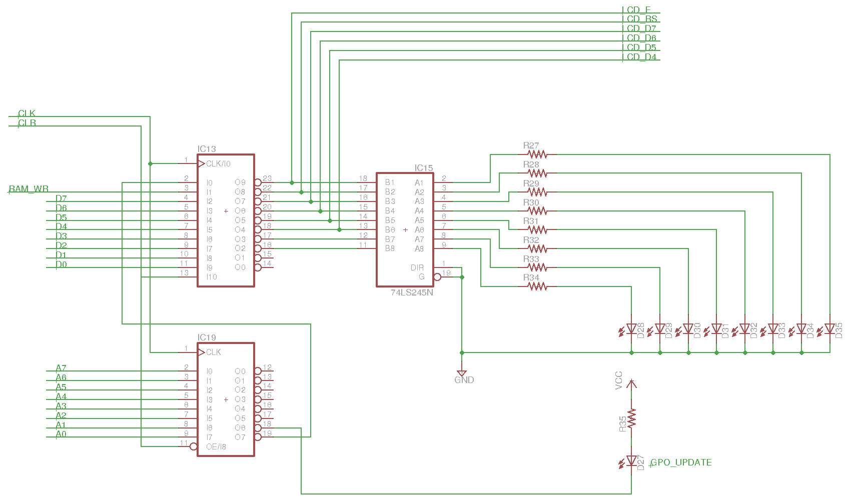
Figure : 38 Control logic circuit
Parts list for the General Purpose Output circuit: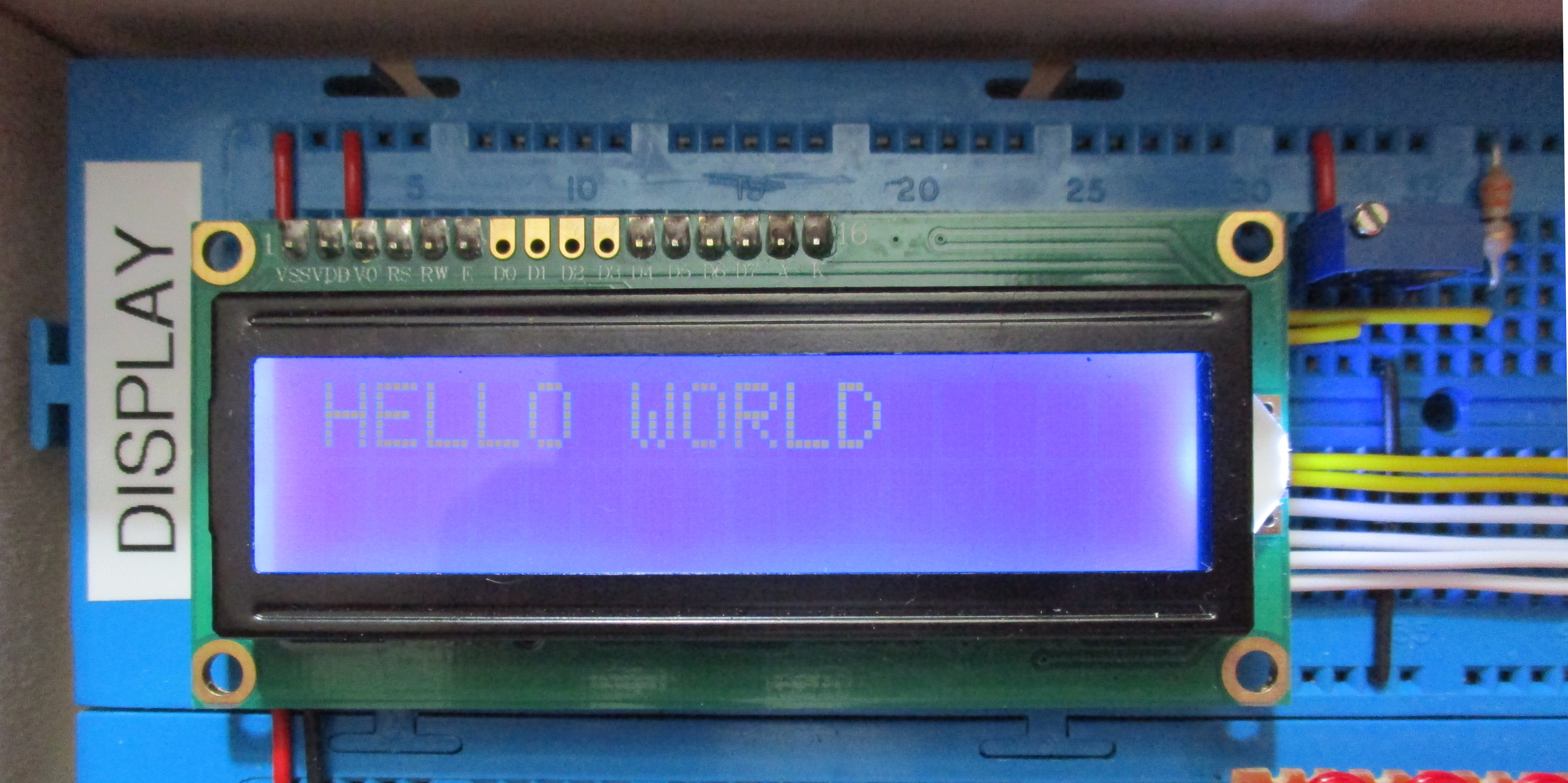
Figure 39 : LCD display
This was a direct port of the code and hardware on this webpage (Link), converting the Python into the simpleCPU assembler below. Basically a lot of GPO outputs to transfer the required information to the LCD. A short video of the computer running the "Hello World" program is available here: (Video). A zoomed in shot of the LCD is available here: (Video). Note, as previously stated a direct port of the code, but i did find that the SPACE character was not displayed correctly i.e. it cleared the display, therefore, used the extended ASCII code 254 which is a blank space, rather than a 'space' which worked fined.
#
# INTERFACE
# ---------

# Pin 23 = Q7;    /* E  */
# Pin 22 = Q6;    /* RS */
# Pin 21 = Q5;    /* D7 */
# Pin 20 = Q4;    /* D6 */
# Pin 19 = Q3;    /* D5 */
# Pin 18 = Q2;    /* D4 */
# Pin 17 = Q1;    /* NU */
# Pin 16 = Q0;    /* NU */

# Initialise display
# ------------------

00 move   0x00 - load ACC with 0
01 store  0xFF - write to output port

# 0011 0011 Initialise
# --------------------

#        E RS D7 D6 | D5 D4 X X
# 0011 - 0 0  0  0  | 1  1  0 0  = 0x0C
# 0011 - 0 0  0  0  | 1  1  0 0  = 0x0C

02 move   0x0C - transfer 0011
03 store  0xFF - write to output port
04 add    0x80 - set E high
05 store  0xFF - write to output port
06 sub    0x80 - set E low
07 store  0xFF - write to output port

08 move   0x0C - transfer 0011
09 store  0xFF - write to output port
10 add    0x80 - set E high
11 store  0xFF - write to output port
12 sub    0x80 - set E low
13 store  0xFF - write to output port

# 0011 0010 Initialise
# --------------------

#        E RS D7 D6 | D5 D4 X X
# 0011 - 0 0  0  0  | 1  1  0 0  = 0x0C
# 0010 - 0 0  0  0  | 1  0  0 0  = 0x08

14 move   0x0C - transfer 0011
15 store  0xFF - write to output port
16 add    0x80 - set E high
17 store  0xFF - write to output port
18 sub    0x80 - set E low
19 store  0xFF - write to output port

20 move   0x08 - transfer 0010
21 store  0xFF - write to output port
22 add    0x80 - set E high
23 store  0xFF - write to output port
24 sub    0x80 - set E low
25 store  0xFF - write to output port

# 0000 0110 Cursor move direction
# -------------------------------

#        E RS D7 D6 | D5 D4 X X
# 0000 - 0 0  0  0  | 1  1  0 0  = 0x00
# 0110 - 0 0  0  1  | 1  0  0 0  = 0x18

26 move   0x00 - transfer 0000
27 store  0xFF - write to output port
28 add    0x80 - set E high
29 store  0xFF - write to output port
30 sub    0x80 - set E low
31 store  0xFF - write to output port

32 move   0x18 - transfer 0110
33 store  0xFF - write to output port
34 add    0x80 - set E high
35 store  0xFF - write to output port
36 sub    0x80 - set E low
37 store  0xFF - write to output port

# 0000 1100 Display On,Cursor Off, Blink Off
# ------------------------------------------

#        E RS D7 D6 | D5 D4 X X
# 0000 - 0 0  0  0  | 1  1  0 0  = 0x00
# 1100 - 0 0  1  1  | 0  0  0 0  = 0x30

38 move   0x00 - transfer 0000
39 store  0xFF - write to output port
40 add    0x80 - set E high
41 store  0xFF - write to output port
42 sub    0x80 - set E low
43 store  0xFF - write to output port

44 move   0x30 - transfer 1100
45 store  0xFF - write to output port
46 add    0x80 - set E high
47 store  0xFF - write to output port
48 sub    0x80 - set E low
49 store  0xFF - write to output port

# 0010 1000 Data length, number of lines, font size
# -------------------------------------------------

#        E RS D7 D6 | D5 D4 X X
# 0010 - 0 0  0  0  | 1  0  0 0  = 0x08
# 1000 - 0 0  1  0  | 0  0  0 0  = 0x20

50 move   0x08 - transfer 0010
51 store  0xFF - write to output port
52 add    0x80 - set E high
53 store  0xFF - write to output port
54 sub    0x80 - set E low
55 store  0xFF - write to output port

56 move   0x20 - transfer 1000
57 store  0xFF - write to output port
58 add    0x80 - set E high
59 store  0xFF - write to output port
60 sub    0x80 - set E low
61 store  0xFF - write to output port

# 0000 0001 Clear display
# -----------------------

#        E RS D7 D6 | D5 D4 X X
# 0000 - 0 0  0  0  | 0  0  0 0  = 0x00
# 0001 - 0 0  0  0  | 0  1  0 0  = 0x04

62 move   0x00 - transfer 0000
63 store  0xFF - write to output port
64 add    0x80 - set E high
65 store  0xFF - write to output port
66 sub    0x80 - set E low
67 store  0xFF - write to output port

68 move   0x04 - transfer 0010
69 store  0xFF - write to output port
70 add    0x80 - set E high
71 store  0xFF - write to output port
72 sub    0x80 - set E low
73 store  0xFF - write to output port

# 1000 0000 LCD RAM address for the 1st line
# ------------------------------------------

#        E RS D7 D6 | D5 D4 X X
# 1000 - 0 0  1  0  | 0  0  0 0  = 0x20
# 0000 - 0 0  0  0  | 0  0  0 0  = 0x00

74 move   0x20 - transfer 1000
75 store  0xFF - write to output port
76 add    0x80 - set E high
77 store  0xFF - write to output port
78 sub    0x80 - set E low
79 store  0xFF - write to output port

80 move   0x00 - transfer 0000
81 store  0xFF - write to output port
82 add    0x80 - set E high
83 store  0xFF - write to output port
84 sub    0x80 - set E low
85 store  0xFF - write to output port

# WRITE CHARACTERS TO DISPLAY

#H  - 0x48
#E  - 0x45
#L  - 0x4C
#L  - 0x4C
#O  - 0x4F

#SP - 0x20

#W  - 0x57
#O  - 0x4F
#R  - 0x52
#L  - 0x4C
#D  - 0x44

# 0100 1000 Print 'H'
# -------------------

#        E RS D7 D6 | D5 D4 X X
# 0100 - 0 1  0  1  | 0  0  0 0  = 0x50
# 1000 - 0 1  1  0  | 0  0  0 0  = 0x60

86 move   0x50 - transfer 0100
87 store  0xFF - write to output port
88 add    0x80 - set E high
89 store  0xFF - write to output port
90 sub    0x80 - set E low
91 store  0xFF - write to output port

92 move   0x60 - transfer 1000
93 store  0xFF - write to output port
94 add    0x80 - set E high
95 store  0xFF - write to output port
96 sub    0x80 - set E low
97 store  0xFF - write to output port

# 0100 0101 Print 'E'
# -------------------

#        E RS D7 D6 | D5 D4 X X
# 0100 - 0 1  0  1  | 0  0  0 0  = 0x50
# 0101 - 0 1  0  1  | 0  1  0 0  = 0x54

98 move   0x50 - transfer 0100
99 store  0xFF - write to output port
100 add    0x80 - set E high
101 store  0xFF - write to output port
102 sub    0x80 - set E low
103 store  0xFF - write to output port

104 move   0x54 - transfer 0101
105 store  0xFF - write to output port
106 add    0x80 - set E high
107 store  0xFF - write to output port
108 sub    0x80 - set E low
109 store  0xFF - write to output port

# 0100 1100 Print 'L'
# -------------------

#        E RS D7 D6 | D5 D4 X X
# 0100 - 0 1  0  1  | 0  0  0 0  = 0x50
# 1100 - 0 1  1  1  | 0  0  0 0  = 0x70

110 move   0x50 - transfer 0100
111 store  0xFF - write to output port
112 add    0x80 - set E high
113 store  0xFF - write to output port
114 sub    0x80 - set E low
115 store  0xFF - write to output port

116 move   0x70 - transfer 1100
117 store  0xFF - write to output port
118 add    0x80 - set E high
119 store  0xFF - write to output port
120 sub    0x80 - set E low
121 store  0xFF - write to output port

# 0100 1100 Print 'L'
# -------------------

#        E RS D7 D6 | D5 D4 X X
# 0100 - 0 1  0  1  | 0  0  0 0  = 0x50
# 1100 - 0 1  1  1  | 0  0  0 0  = 0x70

122 move   0x50 - transfer 0100
123 store  0xFF - write to output port
124 add    0x80 - set E high
125 store  0xFF - write to output port
126 sub    0x80 - set E low
127 store  0xFF - write to output port

128 move   0x70 - transfer 1100
129 store  0xFF - write to output port
130 add    0x80 - set E high
131 store  0xFF - write to output port
132 sub    0x80 - set E low
133 store  0xFF - write to output port

# 0100 1100 Print 'O'
# -------------------

#        E RS D7 D6 | D5 D4 X X
# 0100 - 0 1  0  1  | 0  0  0 0  = 0x50
# 1111 - 0 1  1  1  | 1  1  0 0  = 0x7C

134 move   0x50 - transfer 0100
135 store  0xFF - write to output port
136 add    0x80 - set E high
137 store  0xFF - write to output port
138 sub    0x80 - set E low
139 store  0xFF - write to output port

140 move   0x7C - transfer 1111
141 store  0xFF - write to output port
142 add    0x80 - set E high
143 store  0xFF - write to output port
144 sub    0x80 - set E low
145 store  0xFF - write to output port

# 1111 1110 Print BLANK
# -------------------

#        E RS D7 D6 | D5 D4 X X
# 1111 - 0 1  1  1  | 1  1  0 0  = 0x7C
# 1110 - 0 1  1  1  | 1  0  0 0  = 0x78

146 move   0x7C - transfer 1111
147 store  0xFF - write to output port
148 add    0x80 - set E high
149 store  0xFF - write to output port
150 sub    0x80 - set E low
151 store  0xFF - write to output port

152 move   0x78 - transfer 1110
153 store  0xFF - write to output port
154 add    0x80 - set E high
155 store  0xFF - write to output port
156 sub    0x80 - set E low
157 store  0xFF - write to output port

# 0101 0111 Print 'W'
# -------------------

#        E RS D7 D6 | D5 D4 X X
# 0101 - 0 1  0  1  | 0  1  0 0  = 0x54
# 0111 - 0 1  0  1  | 1  1  0 0  = 0x5C

158 move   0x54 - transfer 0101
159 store  0xFF - write to output port
160 add    0x80 - set E high
161 store  0xFF - write to output port
162 sub    0x80 - set E low
163 store  0xFF - write to output port

164 move   0x5C - transfer 0111
165 store  0xFF - write to output port
166 add    0x80 - set E high
167 store  0xFF - write to output port
168 sub    0x80 - set E low
169 store  0xFF - write to output port

# 0100 1100 Print 'O'
# -------------------

#        E RS D7 D6 | D5 D4 X X
# 0100 - 0 1  0  1  | 0  0  0 0  = 0x50
# 1111 - 0 1  1  1  | 1  1  0 0  = 0x7C

170 move   0x50 - transfer 0100
171 store  0xFF - write to output port
172 add    0x80 - set E high
173 store  0xFF - write to output port
174 sub    0x80 - set E low
175 store  0xFF - write to output port

176 move   0x7C - transfer 1111
177 store  0xFF - write to output port
178 add    0x80 - set E high
179 store  0xFF - write to output port
180 sub    0x80 - set E low
181 store  0xFF - write to output port

# 0101 0010 Print 'R'
# -------------------

#        E RS D7 D6 | D5 D4 X X
# 0101 - 0 1  0  1  | 0  1  0 0  = 0x54
# 0010 - 0 1  0  0  | 1  0  0 0  = 0x48

182 move   0x54 - transfer 0101
183 store  0xFF - write to output port
184 add    0x80 - set E high
185 store  0xFF - write to output port
186 sub    0x80 - set E low
187 store  0xFF - write to output port

188 move   0x48 - transfer 0010
189 store  0xFF - write to output port
190 add    0x80 - set E high
191 store  0xFF - write to output port
192 sub    0x80 - set E low
193 store  0xFF - write to output port

# 0100 1100 Print 'L'
# -------------------

#        E RS D7 D6 | D5 D4 X X
# 0100 - 0 1  0  1  | 0  0  0 0  = 0x50
# 1100 - 0 1  1  1  | 0  0  0 0  = 0x70

194 move   0x50 - transfer 0100
195 store  0xFF - write to output port
196 add    0x80 - set E high
197 store  0xFF - write to output port
198 sub    0x80 - set E low
199 store  0xFF - write to output port

200 move   0x70 - transfer 1100
201 store  0xFF - write to output port
202 add    0x80 - set E high
203 store  0xFF - write to output port
204 sub    0x80 - set E low
205 store  0xFF - write to output port

# 0100 0100 Print 'D'
# -------------------

#        E RS D7 D6 | D5 D4 X X
# 0100 - 0 1  0  1  | 0  0  0 0  = 0x50
# 0100 - 0 1  0  1  | 0  0  0 0  = 0x50

206 move   0x50 - transfer 0100
207 store  0xFF - write to output port
208 add    0x80 - set E high
209 store  0xFF - write to output port
210 sub    0x80 - set E low
211 store  0xFF - write to output port

212 move   0x50 - transfer 0100
213 store  0xFF - write to output port
214 add    0x80 - set E high
215 store  0xFF - write to output port
216 sub    0x80 - set E low
217 store  0xFF - write to output port

218 jump   62
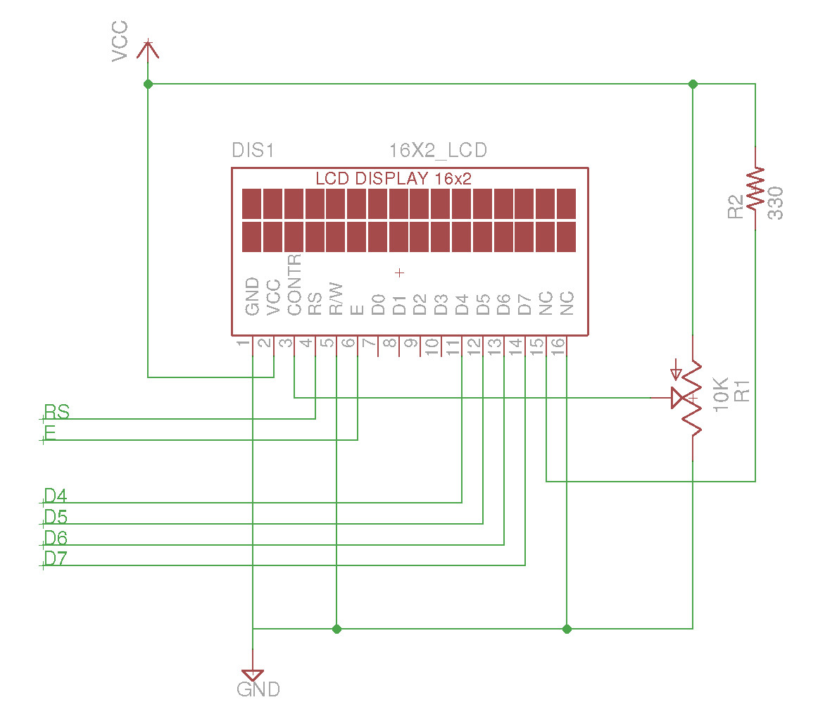
Figure 40 : LCD display circuit
Parts list for the General Purpose Output circuit: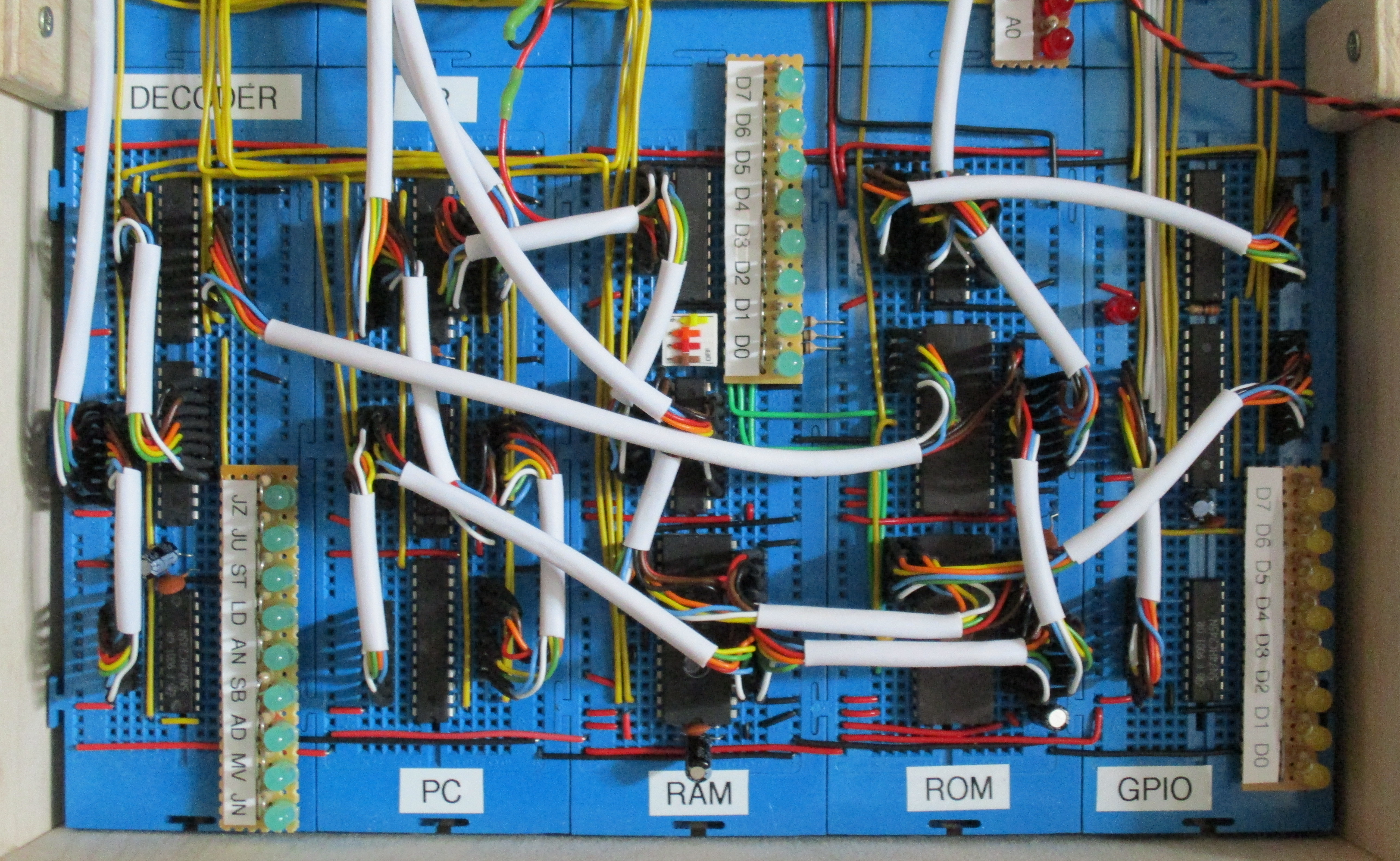
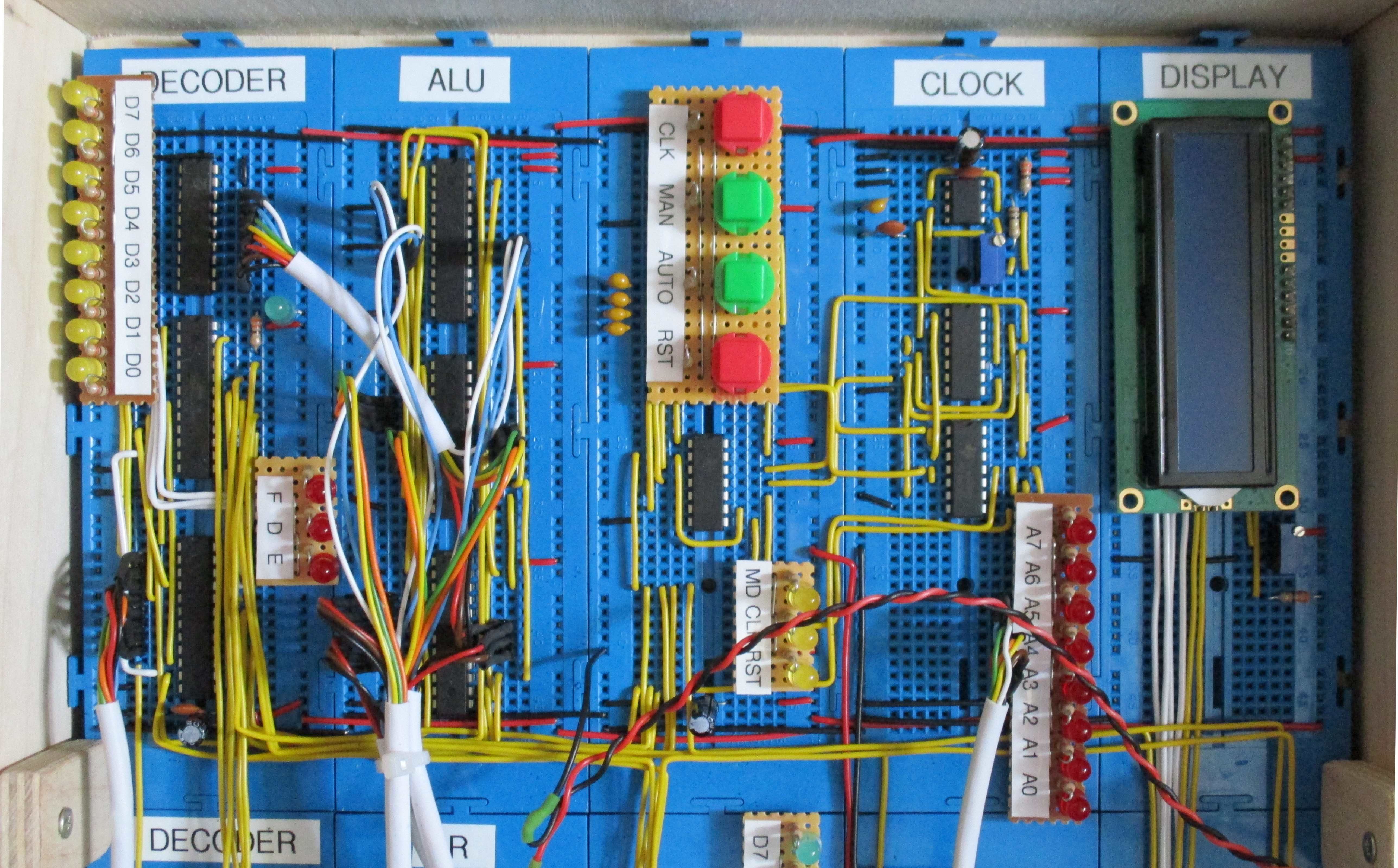
Figure 41: complete system
To try and avoid the lack of testing in version 1 of the simpleCPU came up with the test code below, this exercises most bit combinations and instructions, definitely helped trace down some stuck data lines i.e. wires that had come loose. A short video of the computer running this test program is available here: (Video).
# INSTR   IR15 IR14 IR13 IR12 IR11 IR10 IR09 IR08
# MOVE    0    0    0    0    X    X    X    X
# ADD     0    0    0    1    X    X    X    X
# SUB     0    0    1    0    X    X    X    X
# AND     0    0    1    1    X    X    X    X
# LOAD    0    1    0    0    X    X    X    X
# STORE   0    1    0    1    X    X    X    X
# JUMPU   1    0    0    0    X    X    X    X
# JUMPZ   1    0    0    1    X    X    X    X
# JUMPNZ  1    0    1    0    X    X    X    X

# ACC BIT TEST
# ------------

00 move   0x00
01 move   0x01
02 move   0x02
03 move   0x04
04 move   0x08
05 move   0x10
06 move   0x20
07 move   0x40
08 move   0x80
09 move   0x40
10 move   0x20
11 move   0x10
12 move   0x08
13 move   0x04
14 move   0x02
15 move   0x01

# ADD TEST
# --------

16 add    0xFF - zero ACC
17 add    0xF0 - load high nibble
18 add    0x0F - load low nibble
19 add    0x01 - zero ACC

# SUB TEST
# --------

20 sub    0x01 - set all bits high
21 sub    0xF0 - zero high nibble
22 sub    0x0F - zero low nibble
23 sub    0x01 - set all bits high
24 sub    0x01 - toggle all bits
25 add    0x01
26 sub    0x02
27 add    0x02
28 sub    0x04
29 add    0x04
30 sub    0x08
31 add    0x08

32 sub    0x10
33 add    0x10
34 sub    0x20
35 add    0x20
36 sub    0x40
37 add    0x40
38 sub    0x80
39 add    0x80

# AND TEST
# --------

40 and    0x7F
41 and    0x3F
42 and    0x1F
43 and    0x0F
44 and    0x07
45 and    0x03
46 and    0x01
47 and    0x00

# LOAD / STORE TEST
# -----------------

48 move   0x01
49 store  0x10
50 move   0x02
51 store  0x11
52 move   0x04
53 store  0x12
54 move   0x08
55 store  0x13
56 move   0x10
57 store  0x14
58 move   0x20
59 store  0x15
60 move   0x40
61 store  0x16
62 move   0x80
63 store  0x17

64 load   0x10
65 load   0x11
66 load   0x12
67 load   0x13
68 load   0x14
69 load   0x15
70 load   0x16
71 load   0x17

# GPIO TEST
# ---------

72 move   0x01
73 store  0xFF
74 move   0x02
75 store  0xFF
76 move   0x04
77 store  0xFF
78 move   0x08
79 store  0xFF
80 move   0x10
81 store  0xFF
82 move   0x20
83 store  0xFF
84 move   0x40
85 store  0xFF
86 move   0x80
87 store  0xFF

# JUMP TEST
# ---------

88 move   0x00 - test jump taken
89 jumpZ  91
90 move   0x0F

91 move   0x01
92 jumpNZ  94
93 move   0x0F

94 move   0x00 - test jump not taken
95 jumpNZ  97
96 jump   98
97 move   0x0F

98 move   0x01
99 jumpZ  101
100 jump   102
101 move   0x0F

102 move   0x00
103 jump   0
Note, i think there may be a small issue with the JUMP logic, need to double check, as always 99% of all projects is spent on wiring and testing, otherwise, job done :).
Update 8th August 2019: after a bit more testing i found it was my questionable python programming skills in the assembler that were at fault, a failure to convert three digit decimal numbers correctly (lines 99 and 100), hardware was fine. The second "improvement" is that ive broken the rule that LEDs had to be driven by a separate driver. During a demonstration I wanted to show the complete 16bit instruction that would be fetched from ROM, so that students could see the full progression from raw bit pattern, to decoded instruction, to executed results. Unfortunately, there was no spare space for an additional 74245 driver. Therefore, as a work around i went for some high efficiency blue LEDs, these take significantly less current than the other LEDs allowing me to use 3.9K ohms series resistors rather than the normal 330 ohms i.e. 10 times less. Also as the high byte of the instruction memory only drives the IR these signals are not highly loaded, when compared to the low byte, so it should be fine :). The new and improved display is shown in figure 42.
Figure 42: high byte LEDs

This work is licensed under a Creative Commons Attribution-NonCommercial-NoDerivatives 4.0 International License.
Contact email: mike@simplecpudesign.com