
Figure 1 : Bugs
In SYS1 bugs have googly eyes and are green :), debugging any code is tricky, but debugging assembly code is even more fun :). Testing any code requires that the behaviour of the program can be observed, controlled and then compared against its expected behaviour. The low level nature of assembly code makes this difficult i.e. each instruction doesn't do a lot and may be interacting with other hardware components (peripheral devices) with their own internal state and thread of control e.g. a serial port (UART) etc. To print "Got here" in a high level language such as python is one line of code, for an embedded processor using a low level language requires 10s to 1000s of lines of code, depending on what peripheral devices you are using e.g. serial port or HDMI. Therefore, finding errors in these very long instruction traces is tricky :(
Debugging
Instruction Set Simulators (ISS)
ISS - Breakpoints
ISS - Test Data
ISS - Single Step
ISim
ISim - Breakpoints
ISim - Displaying Bus and Register data
ISim - Test Data
ISim - Debug component
ISim - Visualiser
As always how easy a piece of hardware / software is to debug boils down to a question of testability, which is determined by its:
Designing a system with good controllability and good observability is difficult, sooo, to help solve this problem we can use simulation. This is not a magic bullet, we still have a lot of issues to solve, but it can be a good first step to help identify those "simple" bugs. Next, if required we can consider using test equipment: oscilloscopes, logic analysers etc, to check that our assumptions about how the processor works and real world signals are changing are correct :).
The material below is focused on debugging assembly code for the simpleCPU family of processors, but some of these ideas could be applied to other processors. To illustrate these techniques consider the simpleCPUv1a and simpleCPUv1d test code below. These programs write the values 0-199 and 0-999 to memory, then accumulates this data in TOTAL. The purpose of this code is to produce a lot of "noise", a lot of instructions, a long instruction trace that can be analysed. Using these example programs we will now consider how you would go about test these program, look at how we can simplify different debugging scenarios.
Note, these examples assume you have done SYS1 labs 5 and 6, so are moderately complex :)
##########################
# SimpleCPUv1a Test Code #
##########################

start:
  move 0
  store CNT            # zero CNT

write_loop:
  load CNT             # calc write address
  add DATA
  store 5 write_data
  load CNT             # read data

write_data:
  store start          # write CNT to DATA+CNT
  add 1                # inc CNT
  store CNT
  subm ra N            # is CNT = N?
  jumpnz write_loop    # no repeat

accum:
  move 0
  store TOTAL          # zero TOTAL
  store CNT            # zero CNT

accum_loop:
  load CNT             # calc write address
  add DATA
  store 4 accum_read

accum_read:
  load start           # read DATA+CNT
  addm TOTAL
  store TOTAL

  load CNT
  add 1                # inc CNT
  store CNT
  subm ra N            # is CNT = N?
  jumpnz accum_loop    # no repeat

trap:
  jump trap            # stop

N:
  .data 200            # size of array
TOTAL:
  .data 0              # accumulator total
CNT:
  .data 0              # accumulator total
DATA:
  .data 0              # first address of DATA array
Figure 2 : testcode_v1a.asm
Code is split into two blocks: write (init memory) and accum (calc result). To overcome the limited addressing modes available on the simpleCPUv1a both blocks use self modifying code i.e. the store 5 write_data and store 4 accum_read instructions. These modify the operand bit fields within other instructions to allow the processor to iterate through memory / array. The end of the program is signalled by entering an infinite loop i.e. the is no OS to roll back to, there is no "sleep" instruction.
##########################
# SimpleCPUv1d Test Code #
##########################

start:
  call write           # init DATA array, 0..999
  call accum           # accumulate DATA array, 0+1+2+3+ ... + 999
trap:
  jump trap            # stop

write:
  move rc 0            # rc = data value
  move rb DATA         # rb = data address

write_loop:
  store rc (rb)        # write data to memory
  add rc 1             # inc data value
  add rb 1             # inc data address

  move ra rc           # is value = N?
  subm ra N
  jumpnz write_loop    # no repeat
  ret                  # yes exit

accum:
  move ra 0            # zero TOTAL
  store ra TOTAL
  move rc 0            # rc = loop counter
  move rb DATA         # rb = data address
accum_loop:
  load ra (rb)         # read data value
  addm ra TOTAL        # add TOTAL
  store ra TOTAL       # update TOTAL
  add rc 1             # inc loop counter
  add rb 1             # inc data address

  move ra rc           # is loop counter = N
  subm ra N
  jumpnz accum_loop    # no repeat
  ret                  # yes exit

N:
  .data 1000           # size of array
TOTAL:
  .data 0              # accumulator total
DATA:
  .data 0              # first address of DATA array
Figure 3 : testcode_v1d.asm
As the simpleCPUv1d supports the register indirect addressing mode we do not need to use self-modifying code, also as it supports subroutines we can implement the write and accum blocks as subroutines. Finally, as my adding skills are limited i wrote the python code below just to double check what the totals should be :)
total = 0
for i in range(1000):
    total += i

print( "ACC 0-999 = " + str(total) + " " + hex(total) + " " + hex(total&0xFFFF) )

total = 0
for i in range(200):
    total += i

print( "ACC 0-199 = " + str(total) + " " + hex(total) + " " + hex(total&0xFF) )

Figure 4 : check.py code (top), results (bottom)
Note, the simpleCPUv1a is an 8bit machine sooo looking for a result of 0x00BC, the simpleCPUv1d is an 16bit machine sooo looking for a result of 0x9F2C.
To debug standalone fragments of code perhaps the easiest solution is to use the Instruction Set Simulator (ISS). The previous test code are good examples of such code i.e. short sections of code / subroutines, processing a known data set. Where the ISS has problems is when you have code that needs to interact with other peripheral devices. These hardware components can be approximated in the ISS as a mix of "special" read-write memory and read-only memory e.g. GPIO. However, for more complex components such as UARTs or HDMI controllers this becomes a little tricky. These types of components have their own state and thread of control, therefore, its difficult to produce hardware accurate models of these components i.e. model how a serial terminal or a monitor behaves etc.
The development of the simpleCPU ISS is discussed in more detail on these webpages: (Link), (Link). This simulator can be launched via a GUI, but its easier to launch it via the command line. Before we can simulate this test code we need to assemble it i.e. generate the .dat file. Assuming you are in the ISS folder described in the previous link, to assemble the simpleCPUv1a test program we can execute the command below:
python3 bin/simpleCPUv1a_as.py -i code/testcode_v1a -o code/testcode_v1a
This command generates the required .dat file used by the ISS. To simulate the simpleCPUv1a test program running on the processor we can next run this command:
time python3 bin/simple_cpu_v1a_simulator.py -s2 -r1 -i code/testcode_v1a > dmp

Figure 5 : command (top), results (bottom)
The -s2 switch = full speed, -r1 switch = run to completion i.e. disable user interaction, -i switch is the name of the .dat file to be simulated, all outputs are written to the file: dmp. To run this simulation took 0.03s, the dump file contains a full instruction trace of the instructions executed and a memory dump of the processor's memory when the program executed the "jump trap" instruction i.e. enters an infinite loop at the end of the program, extracts of this file are shown below:
MEMORY MAP
----------
   ADDR           READ                WRITE
0xFF (255)   Port B DATA OUT    Port B DATA OUT
0xFE (254)   Port B DATA IN     Port B DATA OUT
0xFD (253)   Port A DATA OUT    Port A DATA OUT
0xFC (252)   Port A DATA IN     Port A DATA OUT
0xFB (251)   RAM                RAM
...  (...)   ...                ...
0x00 (000)   RAM                RAM

WARNING : this simulator is not guaranteed to be functionally accurate when compared to the HW
Press CTRL-C to stop simulation run
000 : move 0 -> acc:0
001 : store 28 -> M[28]:0
002 : load 28 -> acc:0
003 : add 29 -> acc:29 z:0
004 : store 5 6 -> M[6]:20509
005 : load 28 -> acc:0
006 : store 29 -> M[29]:0
007 : add 1 -> acc:1 z:0

...

017 : load 228 -> acc:199
018 : addm 27 -> acc:188 z:0
019 : store 27 -> M[27]:188
020 : load 28 -> acc:199
021 : add 1 -> acc:200 z:0
022 : store 28 -> M[28]:200
023 : subm 26 -> acc:0 z:1
024 : jumpnz 14 -> False z:1
025 : jumpu 25 -> True
025 : jumpu 25 -> True
    : k=keys, r=run, s=step, v=registers, x=read, w=write, i=input, o=output, q=quit

acc:0 z:1
00: 0000 501c 401c 101d 5506 401c 50e4 1001 501c 701a a002 0000 501b 501c 401c 101d
10: 5411 40e4 601b 501b 401c 1001 501c 701a a00e 8019 00c8 00bc 00c8 0000 0001 0002
20: 0003 0004 0005 0006 0007 0008 0009 000a 000b 000c 000d 000e 000f 0010 0011 0012
30: 0013 0014 0015 0016 0017 0018 0019 001a 001b 001c 001d 001e 001f 0020 0021 0022
40: 0023 0024 0025 0026 0027 0028 0029 002a 002b 002c 002d 002e 002f 0030 0031 0032
50: 0033 0034 0035 0036 0037 0038 0039 003a 003b 003c 003d 003e 003f 0040 0041 0042
60: 0043 0044 0045 0046 0047 0048 0049 004a 004b 004c 004d 004e 004f 0050 0051 0052
70: 0053 0054 0055 0056 0057 0058 0059 005a 005b 005c 005d 005e 005f 0060 0061 0062
80: 0063 0064 0065 0066 0067 0068 0069 006a 006b 006c 006d 006e 006f 0070 0071 0072
90: 0073 0074 0075 0076 0077 0078 0079 007a 007b 007c 007d 007e 007f 0080 0081 0082
a0: 0083 0084 0085 0086 0087 0088 0089 008a 008b 008c 008d 008e 008f 0090 0091 0092
b0: 0093 0094 0095 0096 0097 0098 0099 009a 009b 009c 009d 009e 009f 00a0 00a1 00a2
c0: 00a3 00a4 00a5 00a6 00a7 00a8 00a9 00aa 00ab 00ac 00ad 00ae 00af 00b0 00b1 00b2
d0: 00b3 00b4 00b5 00b6 00b7 00b8 00b9 00ba 00bb 00bc 00bd 00be 00bf 00c0 00c1 00c2
e0: 00c3 00c4 00c5 00c6 00c7 0000 0000 0000 0000 0000 0000 0000 0000 0000 0000 0000
This is big-bang testing at its best, hope for the best testing, if all has gone well one of the memory locations will contain our result: TOTAL, the value 0x00BC. The user can check for this value in the final memory dump, which prints the contents of all memory locations to the screen. The first column is the address in hex i.e. 00, 10, 20 ..., followed by 16, 16bit hex values. Rows containing all zeros i.e. 16 x 0x0000, are not printed. To help the user find the variables they are after the address of each variable can be identified in either the: var.txt, label.txt, or tmp.asm files, that are generated by the assembler.
Note, the files var.txt and label.txt contain the variable/label names + its decimal address in memory. The file tmp.asm contains the assembly language program, the first column is the instructions/variable address, the second is the instruction with any labels replaced with their addresses.
n 26
total 27
cnt 28
data 29
start 0
write_loop 2
write_data 6
accum 11
accum_loop 14
accum_read 17
trap 25
n 26
total 27
cnt 28
data 29
000  move 0
001  store 28 # zero 28
002  load 28 # calc write address
003  add 29
004  store 5 6
005  load 28 # read 29
006  store 0 # write 28 to data+cnt
007  add 1 # inc 28
008  store 28
009  subm ra 26 # is 28 = n?
010  jumpnz 2 # no repeat
011  move 0
012  store 27 # zero 27
013  store 28 # zero 28
014  load 28 # calc write address
015  add 29
016  store 4 17
017  load 0 # read data+cnt
018  addm 27
019  store 27
020  load 28
021  add 1 # inc 28
022  store 28
023  subm ra 26 # is 28 = n?
024  jumpnz 14 # no repeat
025  jump 25 # stop
026  .data 200 # size of array
027  .data 0 # accumulator 27
028  .data 0 # accumulator 27
029  .data 0 # first address of 29 array
Figure 6 : var.txt (top), label.txt (middle), tmp.asm (bottom)
Sooo, TOTAL is stored in address 27 (0x1B) and if we look at this memory location in the final dump file it does indeed contain the value 0x00bc i.e. the correct 8bit accumulated result. This type of testing is ok if your lucky charms are working, however, normally we need to break our testing down into smaller blocks.
The example test program is constructed from two distinct blocks of code: one that initialises data in memory and one that accumulates these values. Therefore, it would be a good idea to unit test these blocks, or at the least test that the first block is writing the correct values to memory. To do this we can use breakpoints i.e. we can pause the simulation and then look at what is stored into memory. A breakpoint is defined using the -b switch, this allows the user to specify an instruction address that if fetched will cause the simulator to pause. Again the address of each label can be identified in the label.txt file produced by the assembler. To test the first block of code in the test program we can next run this command:
time python3 bin/simple_cpu_v1a_simulator.py -s1 -b11 -i code/testcode_v1a
This will cause the simulator to pause at address 11 i.e. the instruction with the label accum, the first instruction of the second block of code. Note, you can define multiple breakpoints by using multiple -b switches. The sequence steps to test if the first block of code is writing the correct values into memory are shown in figure 7 below.


Figure 7 : using breakpoints steps 1-5
To test the second block of code we need data to accumulate, sooo, testing this in isolation is a little more difficult. The simpleCPU simulators do allow you to initialise memory i.e. load an image (.ppm file) and data (.asc file) into memory. However, before we can load a data file we first need to create it :). This test data can be manually created in any text editor, but to simplify this process we can automate this using python.
#######################
# Test data generator #
#######################

def generate_asc(filename, start_addr, value_start, value_end):
  with open(filename, "w") as f:
    value = value_start

    while value <= value_end:
      line_addr = start_addr + value
      line = f"{line_addr:04X}"

      for i in range(16):
        current_value = value + i
        if current_value > value_end:
          break
        addr = start_addr + current_value
        line += f" {current_value:04X}"

      f.write(line + "\n")
      value += 16

generate_asc("output.asc", start_addr=50, value_start=0, value_end=99)
As we are initialising memory we need to the address of our variables e.g. DATA. Again, this can be obtained from the var.txt file, alternatively you can hard code this using the assembler directive .addr. However, buyer beware, you do need to make sure this memory space is free, the assembler trusts that you know what you are doing. To set the DATA variable to start from address 50 we would modify the assembler code as shown below, then run the generate_asc.py program to produce are test data.
start:

accum:
  move 0
  store TOTAL          # zero TOTAL
  store CNT            # zero CNT

accum_loop:
  load CNT             # calc write address
  add DATA
  store 4 accum_read

accum_read:
  load start           # read DATA+CNT
  addm TOTAL
  store TOTAL

  load CNT
  add 1                # inc CNT
  store CNT
  subm ra N            # is CNT = N?
  jumpnz accum_loop    # no repeat

trap:
  jump trap            # stop

N:
  .data 100            # size of array
TOTAL:
  .data 0              # accumulator total
CNT:
  .data 0              # accumulator total
.addr 50
DATA:
  .data 0              # first address of DATA array
0032 0000 0001 0002 0003 0004 0005 0006 0007 0008 0009 000A 000B 000C 000D 000E 000F
0042 0010 0011 0012 0013 0014 0015 0016 0017 0018 0019 001A 001B 001C 001D 001E 001F
0052 0020 0021 0022 0023 0024 0025 0026 0027 0028 0029 002A 002B 002C 002D 002E 002F
0062 0030 0031 0032 0033 0034 0035 0036 0037 0038 0039 003A 003B 003C 003D 003E 003F
0072 0040 0041 0042 0043 0044 0045 0046 0047 0048 0049 004A 004B 004C 004D 004E 004F
0082 0050 0051 0052 0053 0054 0055 0056 0057 0058 0059 005A 005B 005C 005D 005E 005F
0092 0060 0061 0062 0063
To load and simulate this code and data we can next run this command:
time python3 bin/simple_cpu_v1a_simulator.py -s2 -r1 -i code/testcode_v1a2 -l code/output.asc

Figure 8 : simulation output
This example only accumulates 100 values, so as shown in figure 8, the final TOTAL is 0x0056, also note that DATA is also offset to address 50 i.e. 0x32, we have a few more 0x0000 unused memory locations before we see the DATA values 0000, 0001, 0002, 0003 etc.
In the simpleCPUv1d simulator you also have the option of loading a ppm image into memory. This processor has a 12bit address bus, sooo, only having 4096 x 16-bits of memory space does put some limitations on what we can do, consider the examples shown in figure 9.

Figure 9 : Image resolution
As you can see if we were to use a 250 x 219 pixel image, which today would be considered extremely small, we would need to increase the computer's memory size by a factor of 20-ish, used some sort of paging/expanded memory. Therefore, in the test cases we will be processing images will tend to be 30 x 30 pixels. This still allows you to process a simple image, but more importantly for lab work, these smaller images reduce simulation times i.e. you are processing less data, helping reduce debugging times etc.
The image file format is the Portable PixMap (PPM) image format. Originally designed to send images within plain text emails. An example 3 x 3 pixel image using this format is shown in figure 10. The reason for selecting this format is that pixel data can be stored using a simple text format i.e. ASCII characters and can therefore, be edited / viewed using a text editor e.g. Notepad, allowing the user to see how each pixel is represented. Storing data in this format is not very efficient from a file size point of view i.e. would take a lot less space if a binary format was used, however, as the images are only 24 x 24 pixels, this inefficiency is not a significant disadvantage.

Figure 10 : PPM image file (left), displayed image (right)
The first line of the PPM image file identifies the image format to the viewer by its "magic" number P3. This is then followed by a comment/description of the file, indicated by the leading # symbol. The next line defines the image size: columns (width) and rows (height). Lastly, the maximum value of each pixel (255). The remainder of the file defines the RGB value of each pixel, starting at the top left position within the image, a row at a time. These RGB values are listed sequentially in this example, but they could be on different lines, or have multiple RGB values on the same line. However, some image views do seem to insist that you have a blank line at the end.

Figure 11 : Bob 24 x 24 PPM image
Note, you can download this ppm image here: bob.ppm
As the simpleCPU's memory can only store 16bit values, the 24bit RGB data has to be reduced in size, as shown in figure 12. The lower three bits of the RED and BLUE pixel values, and the lower two bits of the GREEN pixel value are removed, to produce a 16bit packed data type. This is done automatically by the simulator when the PPM image is loaded at the start of each simulation i.e. each pixel within the image is loaded into a separate memory location. This again has the advantage of reducing memory usage i.e. a 24 x 24 pixel image can be stored in 576 memory locations.

Figure 12 : packed RGB data format
To process this RGB data the simpleCPU processor will need to extract the original R, G and B values, then left shift these to regenerate the original 8-bit values, as shown in figure 13. The lower bits of these values will be lost, but this should not significantly affect the displayed colour.

Figure 13 : packed RGB data format
To illustrate how these types of images could be processed on the simpleCPUv1d consider the code below:
start:
  move rb PIXELS     # rb = pixel address pointer
  load ra COLOUR     # rc = RED
  move rc ra
  move rd 4          # rd = loop count
loop:
  load ra (rb)       # read pixel address
  store rc (ra)      # update with RED pixel
  add rb 1           # inc pixel address pointer
  sub rd 1           # decrement loop counter
  jumpnz loop        # repeat ?

trap:
  jump trap          # no finish

# 1024 + (14 x 24) + 10  = 1370
# 1024 + (14 x 24) + 11  = 1371
# 1024 + (15 x 24) + 10  = 1394
# 1024 + (15 x 24) + 11  = 1395

PIXELS:
  .data 1370
  .data 1371
  .data 1394
  .data 1395

COLOUR:
  .data 0xF800
This program draws a red noise on the image of Bob shown in figure 11. To load an image into memory you can use the command below:
test python3 bin/simple_cpu_v1d_simulator.py -s2 -r1 -i code/image -p bob
The image of Bob (bob.ppm) is loaded into the simulator memory starting at the base address defined by the variable INPUT_IMAGE_BASE_ADDR, one pixel store in each memory location using the packet RGB image format show in figure 12. When the simulation has finished an output image is written to the file dump_bob.ppm i.e. the input image name preceded with "dump_". The data store in this file is obtained from the base address defined by the variable OUTPUT_IMAGE_BASE_ADDR, using the same image parameters, size etc, as specified in the original input image. The output image for this code is shown in figure 14.

Figure 14 : Red nose Bob 24 x 24 PPM image
The final method to debug a program in the ISS is to single step, or "slow" stepping through your code. To single step through the program i.e. simulate one instruction at a time, allowing the user to see how internal registers and external memory locations have been updated. We can launch the simulator using this command:
time python3 bin/simple_cpu_v1a_simulator.py -s0 -i code/testcode_v1a
This will start the simulator as step-1 in figure 7. Then each time the user presses the s key i.e. step, one instruction is simulated, allowing the user to incrementally step through their program. Using the command switch -s0 sets the simulation speed to one instruction every 0.25 seconds. This may sound fast, but at this speed you can read each instruction as it executes, sooo, if you press the r key i.e. run, the simulator will step through the code for you. If any point you wish to pause the simulator you can press CTRL-C, allowing you to go back to manual single stepping. This method can be combined with breakpoints if needed, so that you can examine how a specific section of the program is working i.e. rather than single stepping through a section of code you are not interested in.
The default simulator used in Xilinx ISE 14.7 is ISim which supports VHDL, Verilog, and mixed‑language simulations i.e. its a Hardware Description Language (HDL) simulator. That's all good, but in SYS1 most of the hardware we designed is defined using schematics, so how are these simulated? The answer is that behind the scenes each schematic is automatically converted into a .vhf file i.e. a VHDL representation, a textual description of the wires and components used in that schematic. These files are then passed to ISim allowing it to perform behavioural, functional and timing verification i.e. your normal FPGA workflow, as shown in figure 15.

Figure 15 : Typical FPGA workflow
Note, i still prefer to use schematics for teaching as these help visualise / illustrate how primitive components i.e. logic gates and flip-flops, are connected together to form higher level functionality e.g. counter etc. Yes everything today is HDL, but that doesn't make it the best way to learn hardware design :).
Soooo, to restate the obvious ISim is a hardware simulator, its not a software simulator such as the Instruction Set Simulators (ISS) we looked at previously (Link). However, to test how a program will function on our games console we need to test how a program works with different hardware components, we are not running a program in isolation, to function correctly it will need to interact with different peripheral devices e.g. GPIO, UART, HDMI etc. Yes, we could add this functionality to our ISS, to turn it into an emulator (Link), to allow it to simulate these peripheral devices, but thats not practical when students are adding their own custom hardware and instructions to the processor, therefore, we do need to use a hardware simulator, we do need to use ISim to test some of our programs.
Note, a good introduction to ISim can be found here: (ug682.pdf)
Before we look at specific software debugging techniques that can be used with ISim i want to quickly go through how ISim is used in a typical FPGA workflow shown in figure 15. In a normal workflow we use different types of simulations to test different things:
In SYS1 the processor hardware is designed by me sooo is perfect, well it should be ok until i discover the next bug :). Therefore, in the majority of cases students will be using existing hardware, will be simulating how their code runs on this hardware, sooo should only need to perform behavioural level simulations. Which is good as these are the quickest simulations. By default the signals shown in the waveform diagram are the top-level IO markers, however, you can drag and drop any signal into the waveform diagram i.e. you have fully observability of any signal in your design.
Note, in functional/timing simulations dragging signals into the waveform diagram can be tricky as the names and signal used in the design are normally lost when a design is synthesised e.g. if a logic circuit is minimised.
Consider the top level schematic from lab 6 shown in figure 16. To simulate this hardware ISim uses the VHDL testbench shown in figure 17.

Figure 16 : top level schematic - computer.sch
LIBRARY ieee;
USE ieee.std_logic_1164.ALL;
USE ieee.std_logic_unsigned.ALL;
USE ieee.numeric_std.ALL;

LIBRARY UNISIM;
USE UNISIM.Vcomponents.ALL;

ENTITY computer_TB IS
END computer_TB;
ARCHITECTURE computer_TB_arch OF computer_TB IS

   -- Top level schematic

   COMPONENT computer
   PORT(
     CLK : IN  STD_LOGIC;
     RST : IN  STD_LOGIC;
     GPI : IN  STD_LOGIC_VECTOR(3 DOWNTO 0);
     GPO : OUT STD_LOGIC_VECTOR(3 DOWNTO 0);
     R : OUT STD_LOGIC;
     G : OUT STD_LOGIC;
     B : OUT STD_LOGIC );
   END COMPONENT;

   -- Wires and Buses

   SIGNAL CLK :  STD_LOGIC;
   SIGNAL RST :  STD_LOGIC;
   SIGNAL GPI : STD_LOGIC_VECTOR(3 DOWNTO 0);
   SIGNAL GPO : STD_LOGIC_VECTOR(3 DOWNTO 0);
   SIGNAL R : STD_LOGIC;
   SIGNAL G : STD_LOGIC;
   SIGNAL B : STD_LOGIC;

BEGIN

   -- Unit Under Test

   UUT: computer_debug PORT MAP(
      CLK => CLK,
      RST => RST,
      GPI => GPI,
      GPO => GPO,
      R => R,
      G => G,
      B => B );

   -- 10MHz Clock generator

   clock : PROCESS
   BEGIN
      CLK <= '0'; wait for 50 ns;
      CLK <= '1'; wait for 50 ns;
   END PROCESS;

   -- Reset signal

   clear : PROCESS
   BEGIN
      RST <= '1'; wait for 150 ns;
      RST <= '0'; wait;
   END PROCESS;

   -- Inputs

   tb : PROCESS
   BEGIN
     GPI <= "0000"; wait for 1000 ns;
     GPI <= "0001"; wait for 1000 ns;
     GPI <= "0011"; wait for 1000 ns;
     GPI <= "0111"; wait for 1000 ns;
     GPI <= "1111"; wait for 1000 ns;
   END PROCESS;

END;
Figure 17 : testbench - computer_tb.vhd
A testbench can be broken down into the following sections:
Note, the ";" symbol defines the end of a statement in a process block, therefore, the assignment operator and wait states could be placed on different lines. They were placed on the same line in this example to improve readability. Remember that the statements inside a process run sequentially.
The UUT and each process run concurrently, consider them to be hardware components and the testbench the PCB that connects them together. As shown in figure 18 when we simulate this schematic the only signals that will be displayed in the waveform diagram will be the top level IO markers: CLK, CLR, GPI, GPO and RGB, which is not that useful when you are trying to debug hardware within the processor or code.

Figure 18 : top level schematic
Fortunately we can manual drag and drop component into the waveform diagram, the only issue is you need to identify the components name and its location in the hierarchy. As an example we would like to look at what the ADDSUB component is doing in the ALU. In ISE we can push down the hierarchy, from the CPU, into the ALU where we can identify the auto assigned name that was given to the ADDSUB component i.e. XLXI_39. Then in ISim drag and drop this component from the "Instance and Process Name" column into the "Name" column in the waveform diagram, this will add all the IO ports and internal signals associated with this component. To view signals click on the restart button and simulate for the desired time interval.


Figure 19 : top level schematic (top), simulation (bottom)
When debugging code, we are more interested the state of internal registers e.g. IR, PC, ACC etc, and perhaps processor bus activity. Again these can be dragged and dropped into the waveform diagram, as shown in figure 20, you can also add dividers (purple bars) by right clicking in the Name column, selecting New Divider. This does help to break up the waveform diagram, help you find / view the correct signals.

Figure 20 : adding processor registers
Being able to see the processor's internal state gives key insights into what is happening on the processor, but its still very easy to get lost in the green squiggles, difficult to understand what part of the program is running in different parts of the waveform diagram. For the simpleCPUv1d processor we can improve the debugging process by reserving one of the registers in the register-file for debugging e.g. RD. This register is now only updated with debugging data, therefore, when this register changes in the waveform diagram is now easy to identify where the program is in its execution and view data / variable values. Consider the modification made to the test code in figure 3 below:
##########################
# SimpleCPUv1d Test Code #
##########################

start:
  move rd 0            # STEP 0
  call write           # init DATA array, 0..999
  move rd 1            # STEP 1
  call accum           # accumulate DATA array, 0+1+2+3+ ... + 999
  move rd 2            # STEP 2

trap:
  jump trap            # stop
Using RD as a "step" counter allows the user to quickly identify what part of the waveform trace is used by what subroutine, or to display variable data etc. The key is to keep the update frequency low, so that it can be easily viewed in the waveform diagram i.e. consider it to be the print("got here") debugging technique of high level languages. This is a quick and useful technique if you can spare a register, which is not always possible e.g. the simpleCPUv1a that only has one register :).
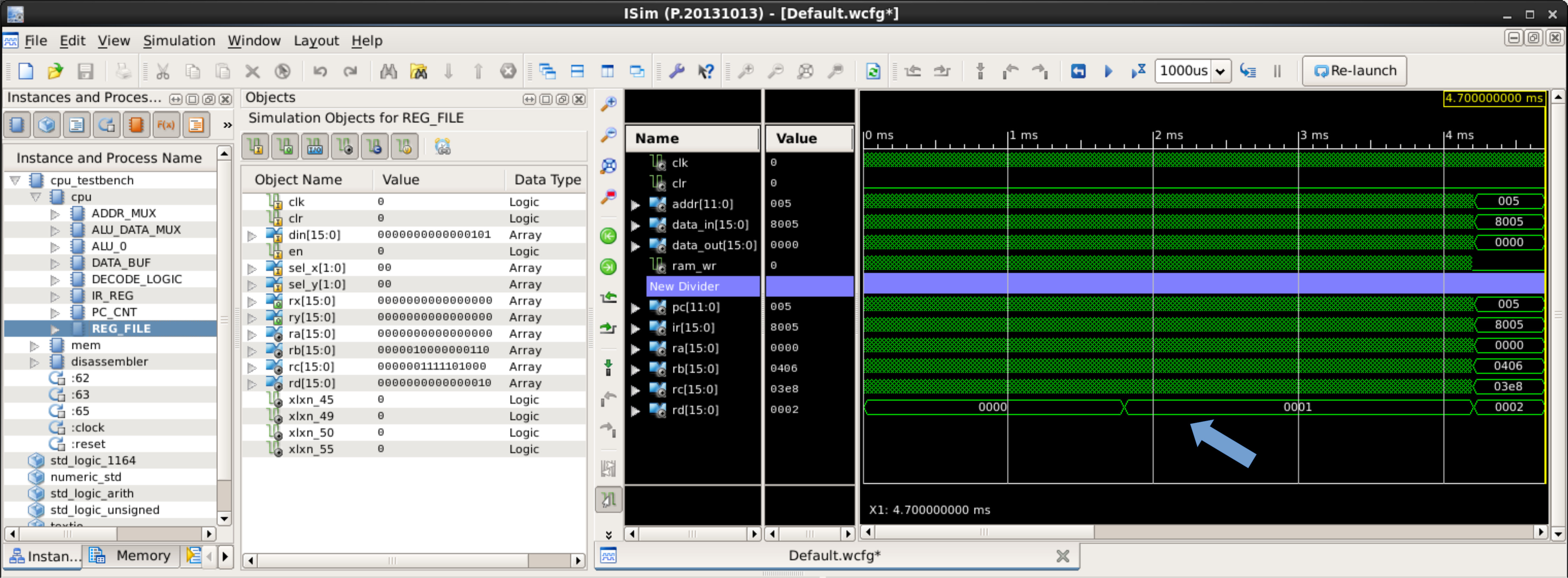
Figure 21 : "debug" register RD
Like the ISS we can observe a program's instruction trace, see how the processors state is changing. This is ok for small programs, but you can quickly get lost with all the green squiggles on the screen. Unfortunately there is not a lot of support in ISim to help debug our programs, however, we can add the VHDL assert and report statements to the testbench to display data in the simulator:
assert TEST report MESSAGE severity LEVEL
The assert TEST should produce a boolean result. Typically a bus or signal is compared to a value e.g. GPO = 0. If the result is FALSE the MESSAGE string is printed in the ISim terminal and its severity LEVEL: note, warning, error, failure. This level is selected by the user, a severity level of failure will halt the simulator i.e. a "breakpoint". These statements can be added to the testbench, after the ARCHITECTURE BEGIN statement:
ARCHITECTURE computer_TB_arch OF computer_TB IS
   ...

BEGIN
   assert to_integer(unsigned(GPO)) = 0 report "GPO = " & integer'image(to_integer(unsigned(GPO))) severity note;

   -- Unit Under Test
   ...
END;
Note, ISim will stop if the assert statement is tagged with a severity of failure, unfortunately you can not then restart Isim :(
GPO is the output bus of the GPIO component controlled by the processor. The ASSERT test first casts the GPO's STD_LOGIC_VECTOR bus to UNSIGNED, then converts this to an INTEGER, which is compared to the value 0. If not zero i.e. the initial value, the REPORT string is printed to the ISim terminal. The string "GPO = " is joined using the "&" concatenation operator with the GPO bus value converted to a string, as shown in figure 22.

Figure 22 : Assert messages
Assert messages are a useful tool to monitor signals and busses in the top-level schematic, but they can't be used to monitor values within a schematic/component e.g. the processor's address bus, or the ACC register inside the processor. ISim does support breakpoints in VHDL, but as the simpleCPU processor is implemented using schematics there is no direct way to use this feature. However, we can add a new breakpoint component, an address monitor PROCESS that is triggered when a breakpoint address is detected on the processor's address bus i.e. the same as the -b switch in the ISS. Consider the breakpoint component below, a copy of this VHDL file can be downloaded here: (breakpoint.vhd)

LIBRARY IEEE;
USE IEEE.STD_LOGIC_1164.ALL;

entity breakpoint is
port (
  A : in std_logic_vector(7 downto 0);
  Y : out std_logic );
end breakpoint;

architecture breakpoint_arch of breakpoint is
begin
   breakpoint_monitor : PROCESS ( A )
   BEGIN
     if to_integer(unsigned(A)) = 11
     then
       Y <= '1';   -- ADD BREAKPOINT ON THIS LINE
     else
       Y <= '0';
     end if;
   END PROCESS;
END breakpoint_arch;
Figure 23 : Breakpoint component (top), VHDL implementation (bottom)
The breakpoint_monitor PROCESS is triggered whenever the A port i.e. the processor's address bus changes. In this example, within the process this value is converted to an integer and then compared to the value 11 i.e. the address of the accum label in figure 2. Within ISim the breakpoint component can be selected from the "Instance and Process Name" column and doubled clicked to open, you can then set a breakpoint by right clicking on the Y <= '1'; statement, selecting toggle breakpoint, that will pause the simulator if executed. This statement is marked with a RED circle to indicate that a breakpoint has been set, as shown in figure 24.

Figure 24 : Adding a breakpoint
The ISim simulation is run as normal, when address 11 is accessed the simulation will be paused i.e. the VHDL for the breakpoint component is opened and a YELLOW arrow indicates where the breakpoint has occurred. The user can then examine the instruction trace and register values displayed in the waveform diagram. To restart the simulation the user simply clicks on the RUN FOR icon. The breakpoint position can also be shown in the waveform diagram for later reference by dragging and dropping the breakpoint component's Y output into the waveform diagram.


Figure 25 : Triggering breakpoint
A similar technique can be used to monitor bus and register values within the processor. To do this we will need to create another new component, the bus_monitor component shown in figure 26, a copy of this VHDL file can be downloaded here: (bus_monitor.vhd)

LIBRARY IEEE;
USE IEEE.STD_LOGIC_1164.ALL;
USE IEEE.STD_LOGIC_UNSIGNED.ALL;

use std.textio.all;
use ieee.std_logic_textio.all;

entity bus_monitor is
generic (
  NAME : string := "ACC";
  SIZE : natural := 8 );
port (
  A : in std_logic_vector(SIZE-1 downto 0) );
end bus_monitor;

architecture bus_monitor_arch of bus_monitor is
  begin
    process( A )
      variable L : line;
    begin
      write(L, now);
      write(L, string'(" : "));
      write(L, NAME);
      write(L, string'(" = "));
      write(L, A);
      writeline(output, L);
    end process;
end bus_monitor_arch;
Figure 26 : bus_monitor component (top), VHDL implementation (below)

Figure 27 : Bus_monitor terminal output
The process in the bus_monitor component is triggered when the signal/bus in its sensitivity list i.e. in the brackets after the key word PROCESS change. VHDL write statements can then be used to construct a text string i.e. a line, that is written to the ISim output terminal. The generic terms can be used to adjust the text NAME and bus SIZE for each instance of the bus_monitor created. However, i confess not sure how you do that in schematics, I've only used generics in VHDL components :).
Test data can be "loaded" into memory by using the .data assembler directive i.e. added to the end of a program. To load values into the FGPA's memory devices i.e. blockRams, is a little more difficult, requires the creation of a memory image component to define the generic parameters in these devices, which as you can guess from that description is not straight forward. Therefore, for simulation / testing purposes, rather than using blockRam based components we can use a VHDL simulation of this memory, a memory device that can automatically load data from files stored on the computer i.e. PC. The interface and main loop of this memory device is shown below, a full copy of this VHDL file can be downloaded here: (ram_4Kx16_sim_v1a.vhd)
use std.textio.all;

Library IEEE;
use IEEE.std_logic_1164.all;
use IEEE.std_logic_unsigned.all;
use IEEE.std_logic_arith.all;

entity ram_4Kx16_sim is
  generic (
    load_file_name      : string  := "iss/code/testcode_v1d.dat";

    load_ppm_image      : boolean := False;
    load_ppm_image_addr : natural := 1024;
    load_ppm_image_name : string  := "iss/image.ppm";

    save_ppm_image      : boolean := False;
    save_ppm_image_addr : natural := 1024;
    save_ppm_image_name : string  := "iss/output.ppm" );
  port (
    CLK      : in  std_logic;
    ADDR_IN  : in  std_logic_vector( 11 downto 0 );
    DATA_IN  : in  std_logic_vector( 15 downto 0 );
    DATA_OUT : out std_logic_vector( 15 downto 0 );
    EN       : in  std_logic;
    WE       : in  std_logic;
    DUMP     : in  std_logic );
end ram_4Kx16_sim;

architecture ram_4Kx16_sim_arch of ram_4Kx16_sim is
begin

  ...

  --
  -- MAIN
  --

  begin
    load_mem( mem );

    if load_ppm_image
    then
      load_ppm( mem );
    end if;

    loop
      if (EN = '1')
      then
        address := conv_integer( ADDR_IN );
        if (WE = '1')
        then
          mem( address ) := DATA_IN;
        end if;
        DATA_OUT <= mem( address );
      end if;

      if (DUMP = '1' and save_ppm_image and not saved)
      then
        saved := True;
        save_ppm( mem );
      end if;

      wait on clk;

    end loop;
  end process;

end ram_4Kx16_sim_arch;
Note, this memory can not be synthesised i.e. implemented on the FPGA, as there is no method to allow such a component to read the PC's filing system.
When the simulation starts, program code is loaded into memory from the specified .dat file. If load_ppm_image is enabled, the specified PPM image is also loaded into memory. When the program has completed it execution it can set the DUMP input high to trigger the PPM image data stored in memory to be written to a file on the PC i.e. output.ppm, allowing the user to view this image.
In addition to using VHDL based components to monitor buses and registers we can use the same techniques to create a disassembler i.e. a component that translates machine-code (binary code) into human readable assembly language, performs the inverse of an assembler, as shown in figure 28.

Figure 28 : debug component
This component monitors the processor's address and data buses, allowing it to capture each instruction's FETCH phase and then disassemble this binary data into the associated assembly language mnemonics i.e. the human readable abbreviations of the machine code instructions. These opcodes and operands are convert into text strings that can be displayed in the waveform diagram. The interface and main loop of this component is shown below, a full copy of this VHDL file can be downloaded here: (debug_v1a.vhd)
LIBRARY IEEE;
USE IEEE.STD_LOGIC_1164.ALL;
USE IEEE.STD_LOGIC_UNSIGNED.ALL;

ENTITY debug IS
PORT (
  CLK  : IN STD_LOGIC ;
  CLR  : IN STD_LOGIC ;
  ADDR : IN STD_LOGIC_VECTOR(7 DOWNTO 0);
  DATA : IN STD_LOGIC_VECTOR(15 DOWNTO 0)  );
END debug;

ARCHITECTURE debug_arch OF debug IS

  TYPE state_type IS (fetch, decode, execute);

  TYPE opcode_type IS (MOVE, ADD, SUB, BW_AND,
                       LOAD, STORE, ADDM, SUBM,
                       JUMP, JUMP_Z, JUMP_NZ,
                       NU, XX );

  SIGNAL opcode : opcode_type;
  SIGNAL imm12  : STD_LOGIC_VECTOR(11 downto 0);
  SIGNAL phase  : state_type ;

BEGIN

  simulation: PROCESS (clk, clr)
    VARIABLE present_state: state_type;
  BEGIN
    IF clr = '1'
    THEN
      present_state := fetch;
    ELSIF clk='1' and clk'event
    THEN
      phase <= present_state;
      CASE present_state IS
        WHEN fetch =>
        present_state := decode;
          CASE DATA(15 downto 14) IS
            WHEN "00" =>
              CASE DATA(13 downto 12) IS
                WHEN "00" =>
                  opcode <= MOVE;
                  imm12 <= "0000" & DATA(7 downto 0);
                ...
                WHEN OTHERS =>
                  opcode <= XX;
                  imm12 <= "XXXXXXXXXXXX";
              END CASE;
            WHEN "01" =>
              CASE DATA(13 downto 12) IS
                WHEN "00" =>
                  opcode <= LOAD;
                  imm12 <= DATA(11 downto 0);
                ...
                WHEN OTHERS =>
                  opcode <= XX;
                  imm12 <= "XXXXXXXXXXXX";
              END CASE;
            WHEN "10"   =>
              CASE DATA(13 downto 12) IS
                WHEN "00" =>
                  opcode <= JUMP;
                  imm12 <= DATA(11 downto 0);
                ...
                WHEN OTHERS =>
                  opcode <= XX;
                  imm12 <= "XXXXXXXXXXXX";
              END CASE;
            WHEN OTHERS =>
              opcode <= XX;
              imm12 <= "XXXXXXXXXXXX";
          END CASE;
        WHEN decode =>
          present_state := execute;
        WHEN execute =>
          present_state := fetch;
        WHEN OTHERS =>
          null;
      END CASE;
    END IF;
  END PROCESS simulation;

END debug_arch;
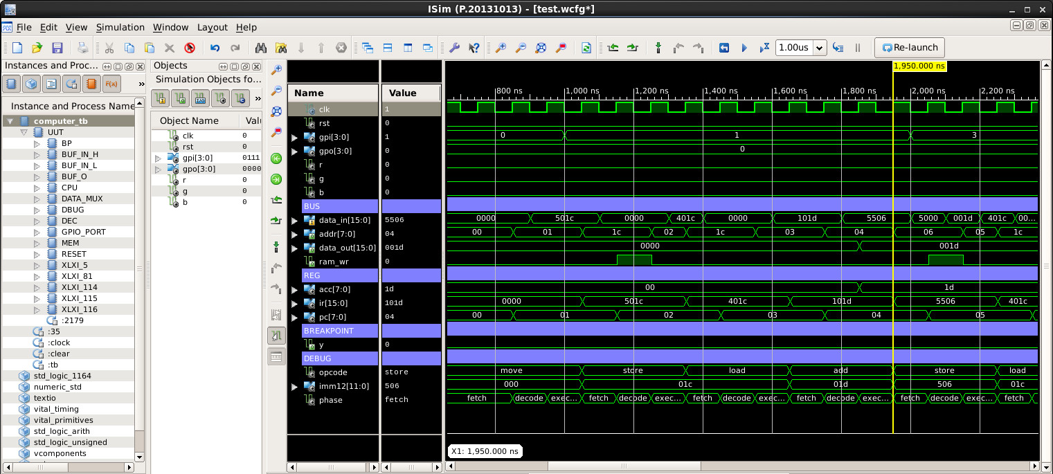
Figure 29 : debug VHDL main loop (top), simulation (bottom)
This makes a waveform diagram a lot easier to understand i.e. you can read what instruction is being executed on the processor, see what data is being processed and how registers and external memory are updated. This combined with breakpoints and some of the other previous techniques provides a reasonable ISim debugging environment.
We can again build upon these ideas and write a python program to visualise a ISim simulator as an instruction trace i.e. comparable to the ISS. The ISim simulation produces a log file: log.txt, recording what instructions have been executed and what variables and stacks (data and call/ret) have been updated. The user can then single step throug this log file i.e. replay the program's execution as if its was an ISS. I would like to take credit for this software, but confess it was a joint effort with Copilot (other AI tools available). This software is mostly AI e.g. the GUI front end etc, but i found that some of the back end stuff was simpler to hand code. This was not by choice, rather i found that if the AI got confused it sometimes would just go off on a rampage and mess up working code. Sooo keeping past versions was essential, development of the code turned into a "choose your battles" developement. If you asked the AI to make a change and it went mad, those changes were done manually, rather than trying to find the perfect prompt to keep the good and change the bad.
The development of this software tool was prompted by the simpleCPUv1d2. This version of the processor was developed to show how the limitation of the simpleCPUv1d could be overcome, how we could create a "practical" processor, a processor that can support typical programming tasks. These improvements are limited to the processor's instruction-set, focusing on usability, rather than redesigning its architecture to increase processing performance, that is done in the simpleCPUv1e :).
The simpleCPUv1d2 has a data stack, a memory structure that can be used to pass arguments to subroutines and return results to the main program. When implementing this stack you either add dedicated hardware support e.g. special purpose registers and instructions (push/pop), or implment this data structure in software i.e. use existing general purpose registers and instructions. As the architecture (hardware) used to implement the simpleCPUv1d2 is fixed i went for a software implementation, comparable to the classic MIPS processor (Link), a RISC processor implementation rather than a CISC implementation.
Note, the CALL/RET stack is still implemented as a hardware stack, contained within the program counter. However, i confess i did increase its depth to 8, as i was finding that i was regularly hitting the previous call depth of 4. Therefore, the software stack is just for passing arguments, creating local variables and returning results. The return address is not stored on this stack it is stored in the hardware stack. A combined stack is implemented later on the simpleCPUv1e :).
When implementing a data stack using the RISC approach it is typical that the stack pointer and frame pointer are implemented using general purpose registers, however, as the simpleCPUv1d2 only has four general purpose registers, using RC for the frame pointer and RD for the stack pointer would be a bit of hit i.e. user code could then only use RA and RB. Therefore, i implemented these pointers as variables:
STACK_START_ADDRESS:
  .data 0xEFF                    # stack start address

STACK_STOP_ADDRESS:
  .data 0xE00                    # stack stop address

STACK_POINTER:
  .data 0xEFF                    # stack pointer

FRAME_POINTER:
  .data 0xEFF                    # frame pointer
This implementation does come with a performance hit i.e. the extra LOAD and STORE instructions need to update these pointers, but it does improve general software performance i.e. allows the user to store working variables in registers. Sooo, this is were the ISim visualiser comes in. When developing the subroutines needed to manage this data stack i found it difficult to follow what was stored on the stack, how the stack and frame pointers where being updated etc. Therefore, i came up with the ISim visualiser, as shown in figure 30.
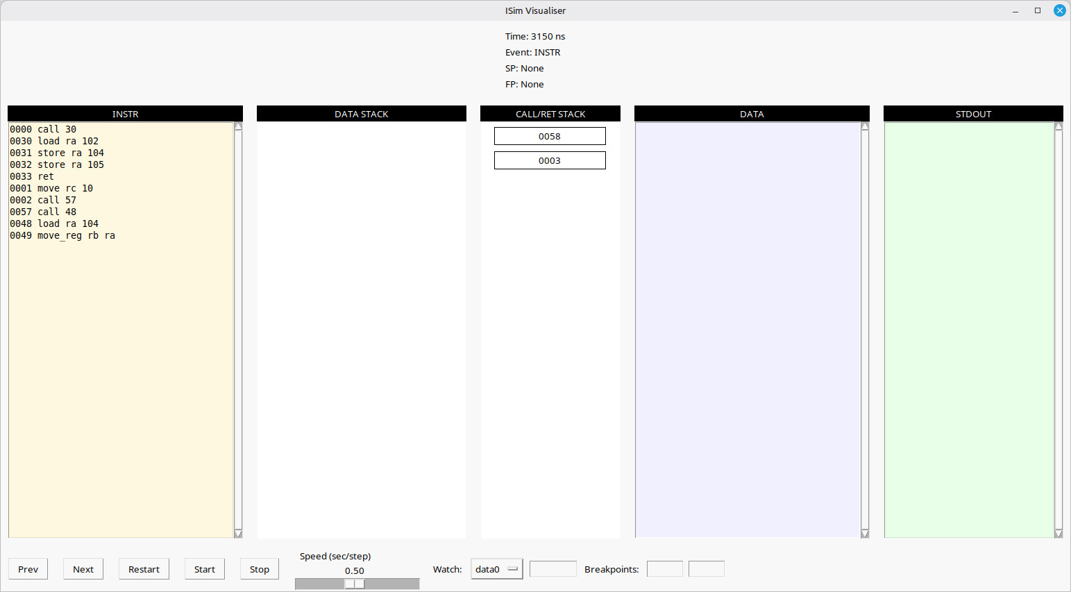
Figure 30 : ISim visualiser
This ISim Visualiser GUI has five panels:
The key panels for debugging the data stack's operation e.g. nested subroutine calls, are the DATA STACK and CALL/RET STACK panels, these update i.e. grow / shrink, as the user steps through the program trace. However, a key thing to remember is that this software is not being simulated in the ISim visualiser, you are simply "replaying" the ISim simulation i.e. the hardware simulation. Therefore, the VHDL debug component has been updated to monitor the processor's ADDR and DATA buses, to disassemble the raw machine code back into assembly language and save this information to: log.txt i.e. recording when an instruction is executed and when a variable or pointer is updated. The ISim visualiser can then process this log file, allow the user to step through this instruction trace. To illustrate this process consider the program below:
test:
  move ra 0                    # zero temp variables
  store ra TMP_LOW
  store ra TMP_HIGH

  call stack_init              # set SP and FP pointer

  move rc 10
  call push16                  # push data to stack

  move rc 20
  call push16                  # push data to stack

  call add16u_stack            # process data

  call pop16                   # pop result off stack
  move ra rc                   # display low word
  store ra STDOUT

  store ra TMP_LOW             # store low result

  call pop16                   # pop result off stack
  move ra rc                   # display high word (carry)
  store ra STDOUT

  store ra TMP_HIGH            # store high result

trap:
  jump trap                    # stop
This program pushes two values onto the stack: 10 and 20. It then calls an ADD subroutine, which pops these values off the stack, adds them together, and pushes the 17bit result to the stack i.e. low and high 16bit values. The main program pops these values off the stack and stores these values to temporary variables and displays them to the user. When the processor hardware and this program are simulated in ISim, the VHDL debug component monitors the processor's ADDR and DATA buses, from this it can identify an instruction's machine code and therefore the assembly language instruction, the variables being accessed and how the CALL/RET and DATA stacks are updated. These events are recorded in the file: log.txt, a section of this programs instruction trace is shown below:
INSTR 450 ns move ra 0  0
INSTR 750 ns store ra 105  1
DATA 800 ns tmp_low 0000
INSTR 1050 ns store ra 106  2
DATA 1100 ns tmp_high 0000
INSTR 1350 ns call 35  3
INSTR 1650 ns load ra 107  35
INSTR 1950 ns store ra 109  36
SP 2000 ns 0EFF
INSTR 2250 ns store ra 110  37
FP 2300 ns 0EFF
INSTR 2550 ns ret  38
INSTR 2850 ns move rc 10  4
INSTR 3150 ns call 62  5
INSTR 3450 ns call 53  62
INSTR 3750 ns load ra 109  53
INSTR 4050 ns move_reg rb ra  54
INSTR 4350 ns ret  55
INSTR 4650 ns store_ind rc rb  63
PUSH 4700 ns 0EFF 000A
INSTR 4950 ns call 46  64

...

INSTR 33150 ns load_ind rc rb  73
POP 33200 ns EFF 001E
INSTR 33450 ns ret  74
INSTR 33750 ns move_reg ra rc  14
INSTR 34050 ns store ra 111  15
STDOUT 34100 ns 0x0000 0
INSTR 34350 ns store ra 106  16
DATA 34400 ns tmp_high 0000
INSTR 34650 ns jumpu 17  17
INSTR 34950 ns jumpu 17  17
Entries in this file are tagged as follows:
INSTR
Instructions executed, format: INSTR TIME OPCODE OPERANDS ADDRESS. The log entry starts with the key word INSTR, signalling that this memory transaction was used to FETCH an instruction, next is the simulation time in nano-seconds and the disassembled assembly language instruction. This can have the format OPCODE, OPCODE OPERAND, or OPCODE OPERAND OPERAND, the number of operands is determined by the OPCODE. The final number is the address of this instruction in memory.
DATA
Data updated i.e. new value written to a variable, format: DATA TIME VAR VALUE. The log entry starts with the key word DATA, signalling that this memory transaction was used to update a variable, next is the simulation time in nano-seconds. Finally the variable name and the value written to it.
SP
Stack pointer updated, format: SP TIME VALUE. The log entry starts with the key word SP, signalling that this memory transaction was used to update the stack pointer variable, next is the simulation time in nano-seconds, finally the value written to it i.e. the address it is pointing to.
FP
Frame pointer updated, format: FP TIME VALUE. The log entry starts with the key word FP, signalling that this memory transaction was used to update the frame pointer variable, next is the simulation time in nano-seconds, finally the value written to it i.e. the address it is pointing to.
PUSH
Stack data updated i.e. new value pushed onto stack, format: PUSH TIME ADDRESS VALUE. The log entry starts with the key word PUSH, signalling that this memory transaction was used to update the stack, next is the simulation time in nano-seconds. Finally the address in memory and the value written to it i.e. position in stack and its data.
POP
Stack data updated i.e. value popped off stack, format: POP TIME ADDRESS VALUE. The log entry starts with the key word POP, signalling that this memory transaction was used to update the stack, next is the simulation time in nano-seconds. Finally the address in memory and the value read from it i.e. position in stack and its data.
STDOUT
Standard out update i.e. new value written to a system variable, format: DATA TIME VAR VALUE. The log entry starts with the key word STDOUT, signalling that this memory transaction was used to update the "display", next is the simulation time in nano-seconds. Finally the value and a 16bit hexadecimal value and a decimal value i.e. the same value but in base 16 and base 10.
This program's execution could be debugged / viewed using ISim's waveform simulator, as shown in figure 31, allowing the user to view memory locations, register, data values etc.
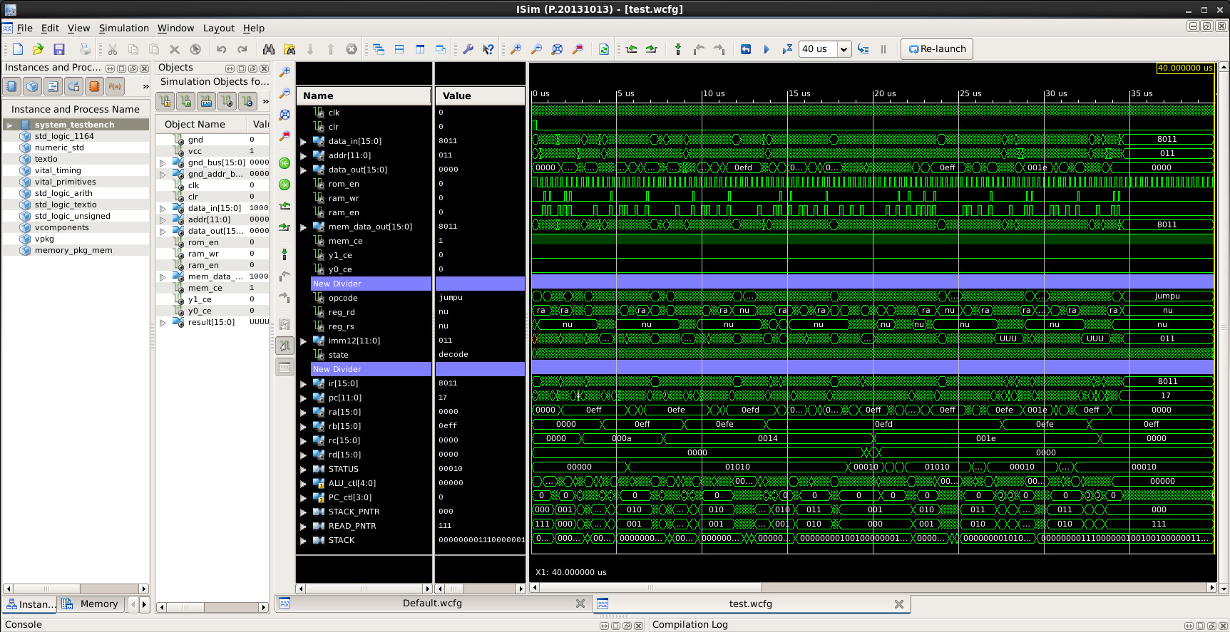
Figure 31 : ISim waveform simulation
This is the main debugging tool for debugging hardware issues as the user can view how data is moving through the processor at the clock cycle level, they can observe the state of any component or signal. However, when debugging software this level of detail makes its difficult to get an overview of what's going on, its very easy to get lost in the waveform. This is where the ISim visualiser comes in, this software removes this noise, allowing the user to view the instructions and see the variables and stack updates as they happen. To illustrate this i made a short video showing how the output of the ISim simulation could be viewed: (Link)
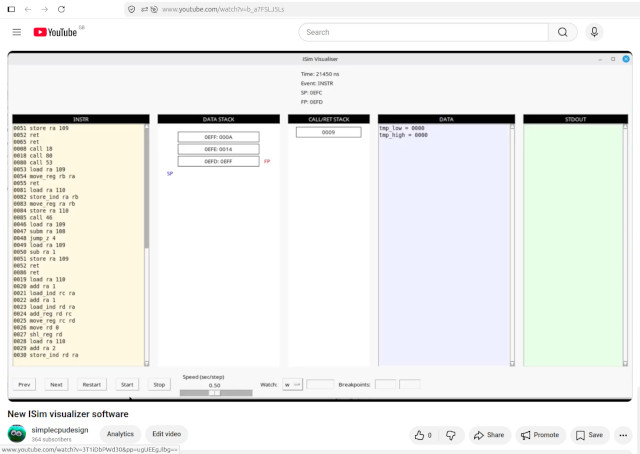
Figure 32 : video of ISim visualiser
Note, just a quick reminder that the ISim visualiser just displays the log file generated during the ISim simulation. It is not an instruction-set simulator. The log file is generated by the VHDL debug component. This monitors the processor's ADDR, DATA and CTL busses i.e. it can not read the internal state of the processor or its memory, it can not see the state of internal components such as the register file, program counter, instruction register etc.
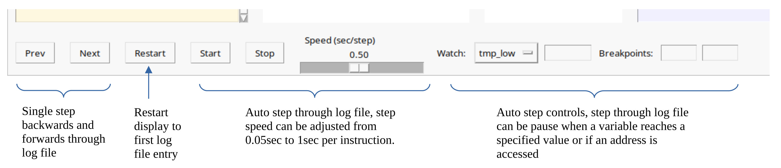
Figure 33 : ISim visualiser controls
The ISim visualiser automatically opens the file: log.txt, the user can then use the controls shown in figure 33 to single-step or auto-step through this log file. Signal step operations are via the Prev and Next buttons. Remember this GUI is just displaying entries in the log file, therefore, there are no state issues related to clicking the Prev or Restart buttons, the software does not need to undo memory writes / updates etc, it is simply displaying values in the log file. An alternative to single stepping is click Start and auto-step. The speed that the visualiser steps through log entries can be controlled by the slide bars: 0.05sec - 1.0sec per step, 0.5sec is a good starting point. When auto-stepping the user can stop these updates by pressing the Stop button, or via the watch or breakpoint options. The watch pulldown menu allows the user to select a variable defined in the program, they can then specify a trigger value. When this variable is assigned that variable, auto-stepping is stopped e.g. useful when analysing loops, stop when a loop count reaches its final value etc. Alternatively, the user can specify two breakpoint addresses, when a log entry for an instruction fetch is displayed, with a matching address auto-stepping is stopped.
More testing, a slightly more complex example, a recursive Fibonacci number generator. Video: (Link)
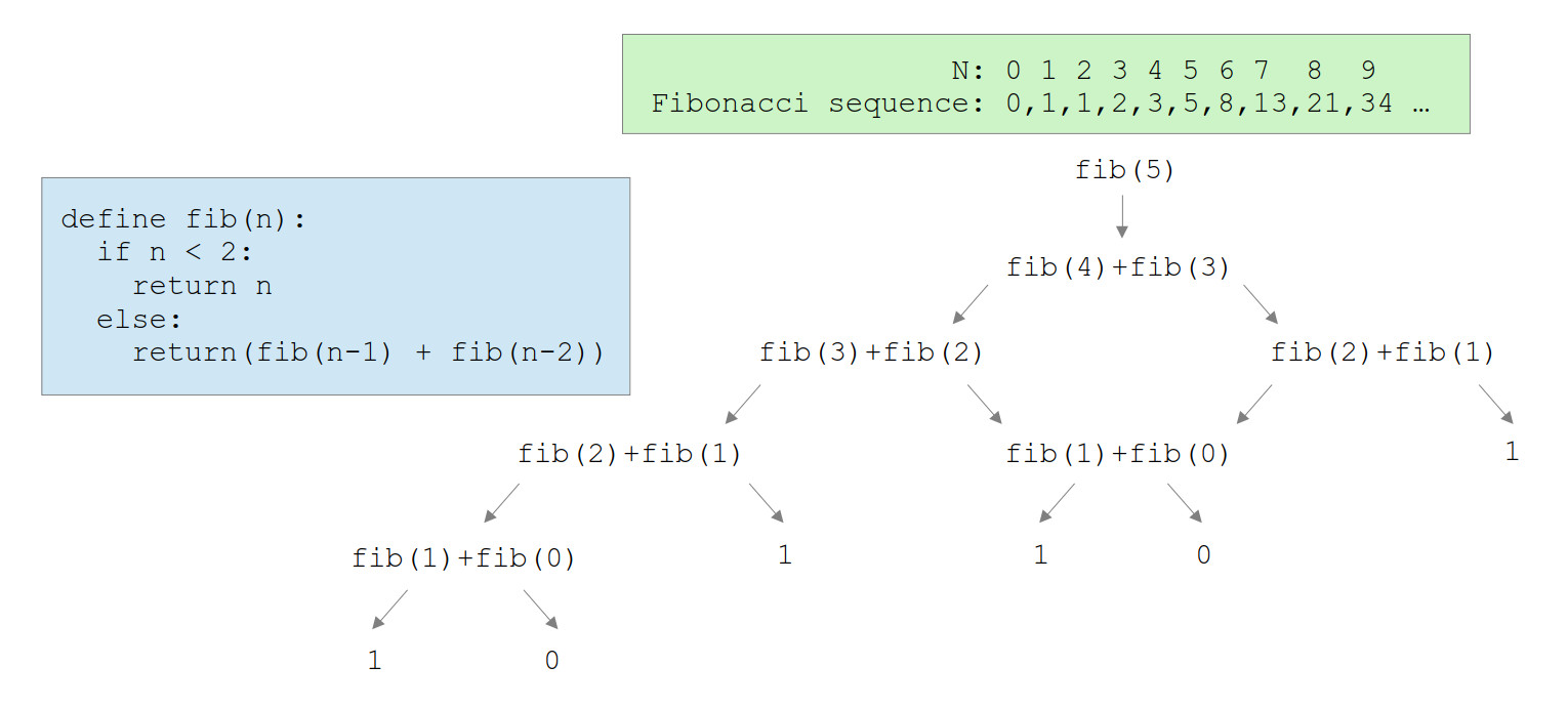
Figure 34 : a recursive Fibonacci number generator algorithm
######################
# Fibonacci sequence #
######################

#########
# STACK #
#########

#        -------------
#        |           |
#        -------------
#        |     N     |
#        -------------
#  FP -> |   OLD FP  |
#        -------------
#        | LOCAL VAR |
#        -------------
#  SP -> |           |
#        -------------

#############
# USER CODE #
#############

start:
    call stack_init         # set SP and FP pointer
    load ra N
loop:
    move rc ra

    call push16             # push N onto stack
    call fib                # call function
    call pop16              # get result

    move ra rc
    store ra STDOUT         # write to STDOUT

    load ra N               # decrement N
    sub ra 1
    store ra N
    jumpp loop             # repeat if not zero

trap:
    jump trap               # stop program

#############
# USER DATA #
#############

N:
    .data 6

########################
# FIBONACCI SUBROUTINE #
########################

fib:
    call stack_create_frame # save old FP to stack
                            # update FP to top of stack

    move rc 0               # create local variable
    call push16

    load ra FRAME_POINTER   # generate address to access N
    add ra 1
    load ra (ra)

    sub ra 2                # test exit condition N<2
    jumpn fib_exit

fib_calc:
    load ra FRAME_POINTER   # generate address to access N
    add ra 1
    load ra (ra)            # load N
    sub ra 1                # N-1
    move rc ra

    call push16             # push N-1 onto stack
    call fib                # call function
    call pop16              # get fib() result

    load ra FRAME_POINTER   # generate address of local VAR
    sub ra 1
    store rc (ra)           # save result in local variable

    add ra 2                # generate address to access N
    load rc (ra)            # load N
    sub rc 2                # N-2

    call push16             # push N-2 onto stack
    call fib                # call function
    call pop16              # get fib() result

    load ra FRAME_POINTER   # generate address of local VAR
    sub ra 1
    load rb (ra)            # load result from local variable
    add rc rb               # add first and second fib() result
    add ra 2
    store rc (ra)           # overwrite N with result

 fib_exit:
    call stack_remove_frame #
    ret
Figure 35 : video of ISim visualiser
WORK IN PROGRESS

This work is licensed under a Creative Commons Attribution-NonCommercial-NoDerivatives 4.0 International License.
Contact email: mike@simplecpudesign.com