I finally decided to implement a Hardware Description Language (HDL) version of the simpleCPU version 1a. I confess i don't have a good explanation for why i did not do this years ago as my background is in electronics and most of my research career was spent designing custom hardware for FPGAs using HDLs. I guess as always there is never enough time to do the fun things :). Back in the past, when i actually designed actual hardware, my HDL of choice was VHDL: Very High Speed Integrated Circuit Hardware Description Language (Link). The reason for this choice was that back then the Department of Comp. Sci. at York was famous for its Ada compiler, therefore, i had done a lot of software work in Ada (Link). VHDL is based on Ada, as both languages were commissioned by the United States Department of Defence (DoD), so switching from software to hardware, putting back on my electronics engineer's hat, i found VHDL a very easy language to pickup. A HDL i never really looked at was Verilog (Link), no good reason other than it wasn't VHDL :). I guess you could also add to this list System Verilog. Therefore, as Verilog is now the more popular HDL on the market i thought it was time to learn the basics, and as always its always easier to learn stuff whilst applying this knowledge to a practical problem, so why not implement the simpleCPU. Below is a guide to how to build the simpleCPU version 1a in both VHDL and Verilog. Note, it will be interesting at the end to see which language produces the "best" hardware i.e. smallest / fastest implementation :).
SimpleCPU v1a
NOR gate
Multiplexers
Arithmetic and Logic Unit
Registers and counters
Control logic
Memory
Computer and testing
FPGA board
Figure 1 : simpleCPU version 1a block diagram
The VHDL and Verilog implementations of the simpleCPUv1a block diagram shown in figure 1 will follow the same design approach as the previous schematic implementations i.e. functionality is broken down into a series of sub-components, which are then used to build larger components, which in turn form the key building blocks of the processor's architecture. Note, well that was the plan, confess looking back at the end i did use a couple of higher level descriptions to save some time i.e. abstract descriptions. A brief intro into the VHDL and Verilog languages can be found here: (Link) (Link).
WARNING : the discussion below are my opinions not necessarily facts :), i am not a Verilog programmer, my background is in VHDL, so rather these are my observations on the differences between these two HDLs. This is not a tutorial on how to use VHDL or Verilog, rather these are notes and examples for me so i don't forget stuff later :).
So to start this journey we will start simple: basic logic gates. To detect if the ACC is zero the simpleCPU uses an eight input NOR gate, one possible VHDL and Verilog implementation is shown below.
VHDL
----

library IEEE;
use IEEE.STD_LOGIC_1164.ALL

entity NOR_8
port(
  A : in  STD_LOGIC_VECTOR( 7 downto 0 );
  Z : ou STD_LOGIC);
end entity;
architecture NOR_8_ARCH of NOR_8 is
begin
  Z <= NOT( A(7) OR A(6) OR A(5) OR A(4) OR A(3) OR A(2) OR A(1) OR A(0) );
end NOR_8_ARCH;

VERILOG
-------

STYLE 1
-------
module NOR_8( A, Z );
  input [7:0] A;
  output Z;
  assign Z = ~( A[7] | A[6] | A[5] | A[4] | A[3] | A[2] | A[1] | A[0] );
endmodule

STYLE 2
-------
module NOR_8(
  input [7:0] A,
  output Z );
  assign Z = ~( A[7] | A[6] | A[5] | A[4] | A[3] | A[2] | A[1] | A[0] );
endmodule

STYLE 3
-------
module NOR_8(
  input [7:0] A,
  output reg Z );

  always @(*) begin
    Z = ~( A[7] | A[6] | A[5] | A[4] | A[3] | A[2] | A[1] | A[0] );
  end
endmodule
VHDL supports the Boolean operators: NOT, AND, NAND, OR, NOR, XOR, XNOR. Verilog supports the same Boolean operators: !, &, ~&, |, ~|, ^, ~^. Apart from syntax the first difference i noticed is that VHDL uses an additional library to support multi-valued logic i.e. VHDL natively supports the type bit: {0,1}, but to support other states such as high-impedance, not-connected, or weak signals etc, you need to import the STD_LOGIC libs. These support 9 distinct logic states {0,1,U,X,Z,W,L,H,-}. Verilog supports multi-valued logic built-in, but only uses 4 distinct logic states {0,1,X,Z}, but these do cover 99% of the basic scenarios.
Verilog has a few different "styles", as shown by the three examples above. Confess, not sure why you need style-1. I would describe these styles of HDL as behavioural i.e. not structural. However, this is a low level description, you are defining functionality in terms of logic gates, so i guess these will always look similar, i guess you could say these examples use a dataflow style. A key point to note in these Verilog descriptions is the "assign" keyword, this alters the meaning of "=" symbol, it defines a continuous assignment, no dependency on a clock, or sequential behaviour i.e. it is not a blocking assignment, it is just logic. Similarly, style-3 the "reg" declaration in the output definition does not mean "registered", the "*" in the sensitivity list redefines this as meaning "assigned" i.e. logic. I don't like this inconsistency :(. Finally, why isn't there a ';' after endmodule?
You can download copies of these files as a ISE project with a testbench here: (Link). Note, the .vhd and .v files need to be manually added to the project one at a time for testing as they use the same name. From these HDL descriptions the Xilinx ISE tools can create an RTL schemtic, as shown in figure 2. A waveform diagram of this component in action is shown in figure 3 below.
Figure 2 : NOR gate schematic
Figure 3 : NOR gate simulation
Rather than implementing this components from basic logic gates i.e. AND, OR and NOT (Link) i decided to build this component using a higher level, abstract HDL description, one possible VHDL and Verilog implementation is shown below.
VHDL
----

library IEEE;
use IEEE.STD_LOGIC_1164.ALL;

entity MUX_2_8 is
Port (
    A, B : IN  STD_LOGIC_VECTOR(7 downto 0);
    SEL  : IN  STD_LOGIC;
    Y    : OUT STD_LOGIC_VECTOR(7 downto 0));
end MUX_2_8;

architecture MUX_2_8_ARCH of MUX_2_8 is
begin
    Y <= B when SEL = '1' else A;
end MUX_2_8_ARCH;

VERILOG
-------

module MUX_2_8 ( A, B, SEL, Y );
  input [7:0] A;
  input [7:0] B;
  input SEL;
  output [7:0] Y;
  assign Y = SEL ? B : A;
endmodule
Unlike the previous examples the HDL style used here is definitely not structural, as we are not defining the hardware's functionality in terms of Boolean logic. Most people would describe this style as dataflow, but i would tend to use the more general term of Behavioural. Confess, i don't normally use the syntax shown here i.e. select statements, i would use a PROCESS in VHDL i.e. IF-THEN-ELSE, we will see these in a bit. However, this does highlight another difference between VHDL and Verilog i.e. assignments and the use of the different "=" symbols.
In VHDL "<=" is read as driven e.g. Y <= A, would read as Y is driven by A. These are signals i.e. A and Y would be "wires" in the real world. In VHDL the "=" symbol is a relational operator i.e. equals, returning a Boolean. You do have the concept of variables in VHDL and assignments to these use ":=" e.g. Y := A would read as Y is assigned A. These are variables i.e. Y and A are used in abstract high-level hardware descriptions. These focus on describing the hardware's function, not its implementation, therefore, a variable could represent integers, floats, arrays etc, they don't have to be a "hardware" specific data type, they don't have to directly model real-world hardware.
In Verilog "=" is a blocking assignment and "<=" is a non-blocking assignment. These are used within a procedural block, which we will look at later. However, as we have already seen the "assign" keyword alters the reading of the "=" assignment to mean continuous i.e. it is logic. So using the "assign" keyword means it is neither blocking or non-blocking, which is not at all confusing :). The term "blocking" refers to how an assignment is performed. A blocking assignment must complete before the next HDL instruction is executed e.g. if you had instructions Y = 10 and the next instruction was A = Y, then A = 10. This would be the same for a VHDL variable. That seems logical, but that's how software behaves, not hardware, signals do not update instantaneously, there will be wire and propagation delays to consider. Therefore, in Verilog we have non-blocking assignments i.e. "<=" operator, these allow multiple assignments to operate in parallel, allows assignments to be scheduled / updated at the end of a simulation time step. The "==" is a relational operator i.e. equals, returning a Boolean.
Note, the concept of blocking and non-blocking assignments is confusing :). In VHDL we would now start to talk about delta cycles, start to think about how the simulator actually works. Consider what happens in a simple combinatorial logic circuit i.e. all logic gates will be working in parallel. The order these gates are simulated in the simulator must not affect the simulation result. Yes there is a "sequential" behaviour as signals propagate through a circuit, but each gate could have different propagation delays. Updates to their outputs and the "wires" they are connected to need to be scheduled in the simulator i.e. at different times. Therefore, a signal could go through multiple transitory states before settling down to a stable value. A blocking assignment does not consider this, it will be performed instantaneously within the simulator, which is not what will happen in a real-world circuit. Therefore, like VHDL, blocking assignments i.e. variables, should only be used in a PROCESS, a high-level sequential description of what a piece of hardware does, or in simple logic circuits such as the previous NOR gate example i.e. HDL descriptions with a single assignment, or logic where the output of one assignment is NOT used as the input of another. Yes, there are always exceptions to these rules, BUT, i'm always very careful where and how i use blocking assignments i.e. i try to avoid them, as you could end up with a hardware description that does not describe the hardware behaviour you want :(.
You can download copies of these files as a ISE project with testbench here: (Link). Note, the .vhd and .v files need to be manually added to the project one at a time for testing as they use the same name. From these HDL descriptions the Xilinx ISE tools can create an RTL schemtic, as shown in figure 4. A waveform diagram of this component in action is shown in figure 5 below.
Figure 4 : MUX schematic
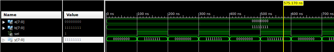
Figure 5 : MUX simulation
Basically a direct copy of the original design (Link), just implemented as a higher level, abstract HDL description. The first component constructed is the adder / subtract unit, one possible VHDL and Verilog implementation is shown below.
VHDL
----

library IEEE;
use IEEE.STD_LOGIC_1164.ALL;
use IEEE.STD_LOGIC_UNSIGNED.ALL;

entity ADDSUB_8 is
port (
  A, B : in  STD_LOGIC_VECTOR(7 downto 0);
  SEL  : in  STD_LOGIC;
  Y    : out STD_LOGIC_VECTOR(7 downto 0);
  C    : out STD_LOGIC );
end ADDSUB_8;

architecture ADDSUB_8_ARCH of ADDSUB_8 is
    signal b_int : STD_LOGIC_VECTOR(7 downto 0);
    signal y_int : STD_LOGIC_VECTOR(8 downto 0);
begin
    b_int <= B when SEL = '0' else not B;
    y_int <= ("0" & A) + ("0" & b_int) + Sel;

    Y <= y_int(7 downto 0);
    C <= y_int(8);
end ADDSUB_8_ARCH;

VERILOG
-------

module ADDSUB_8( A, B, SEL, Y, C );
  input [7:0] A;
  input [7:0] B;
  input SEL;
  output [7:0] Y;
  output C;

  wire [7:0] b_int;
  wire [8:0] y_int;

  assign b_int = SEL ? ~B : B;
  assign y_int = A + b_int + SEL;

  assign Y = y_int[7:0];
  assign C = y_int[8];
endmodule
I tried to follow on from the MUX example and use the "select" instructions to switch between the inverted and non-inverted input i.e. 2s complement conversion. When performing addition the result of two n-bit numbers will be n+1 bits i.e. there could be a carry. In VHDL bus bit-widths must match, therefore, you need to pad buses with a leading zero i.e. for the sign bit. This is achieve in VHDL using the concatenation operator "&". Note, in Verilog concatenation is performed using "{ }" e.g. {0, A}. In Verilog if bus sizes do not match, the shorter bus will be automatically sign-extended. Note, interestingly in Verilog you do not define how ADD is performed i.e. signed or unsigned etc. From these HDL descriptions the Xilinx ISE tools can create an RTL schemtic, as shown in figure 6. A waveform diagram of this component in action is shown in figure 7 below.
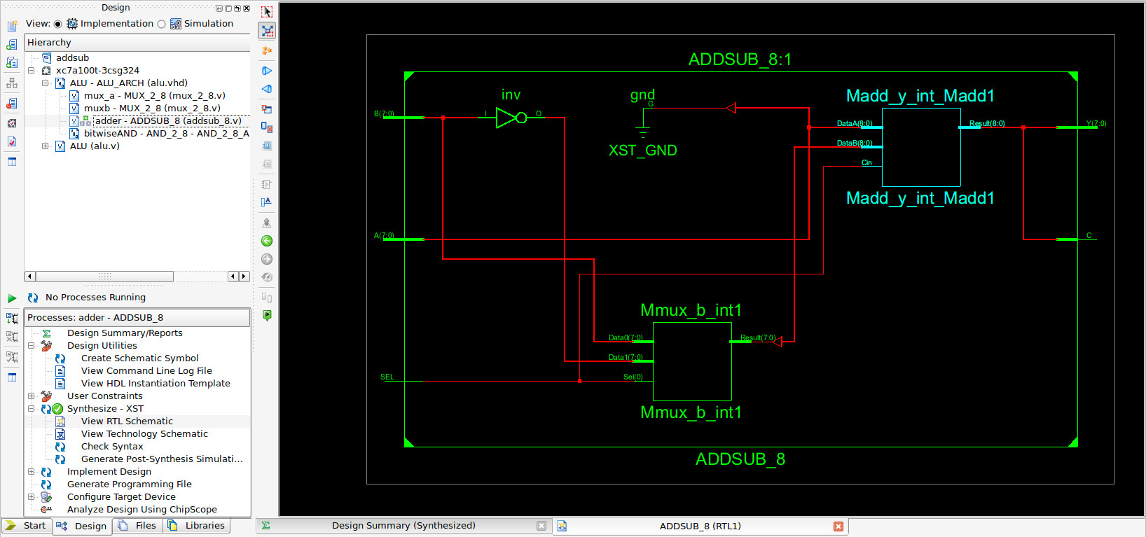
Figure 6 : ADDSUB schematic
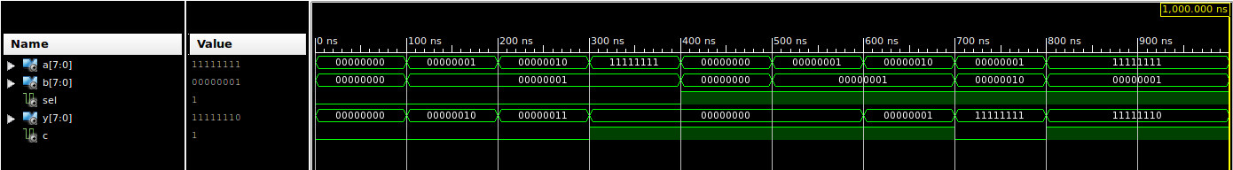
Figure 7 : ADDSUB simulation
In addition to the ADDSUB component the ALU also has a bit-wise AND, one possible VHDL and Verilog implementation is shown below.
VHDL
----

library IEEE;
use IEEE.STD_LOGIC_1164.ALL;

entity AND_2_8 is
port(
  A : IN  STD_LOGIC_VECTOR( 7 downto 0 );
  B : IN  STD_LOGIC_VECTOR( 7 downto 0 );
  Z : OUT STD_LOGIC_VECTOR( 7 downto 0 ) );
end AND_2_8;

architecture AND_2_8_ARCH of AND_2_8 is
begin

  Z(7) <= A(7) AND B(7);
  Z(6) <= A(6) AND B(6);
  Z(5) <= A(5) AND B(5);
  Z(4) <= A(4) AND B(4);
  Z(3) <= A(3) AND B(3);
  Z(2) <= A(2) AND B(2);
  Z(1) <= A(1) AND B(1);
  Z(0) <= A(0) AND B(0);

end AND_2_8_ARCH;

VERILOG
-------

module AND_2_8( A, B, Z );
  input [7:0] A;
  input [7:0] B;
  output [7:0] Z;

  assign Z[7] = A[7] & B[7];
  assign Z[6] = A[6] & B[6];
  assign Z[5] = A[5] & B[5];
  assign Z[4] = A[4] & B[4];
  assign Z[3] = A[3] & B[3];
  assign Z[2] = A[2] & B[2];
  assign Z[1] = A[1] & B[1];
  assign Z[0] = A[0] & B[0];

endmodule
No surprises here the AND_2_8 component uses the same style / code as the NOR_8. From these HDL descriptions the Xilinx ISE tools can create an RTL schemtic, as shown in figure 8. A waveform diagram of this component in action is shown in figure 9 below.
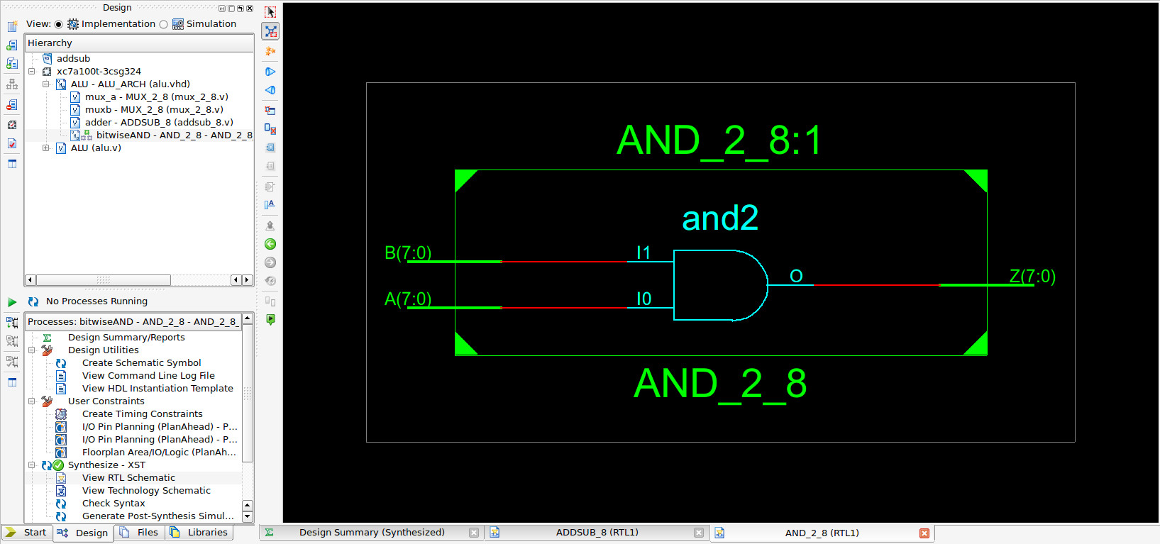
Figure 8 : AND schematic
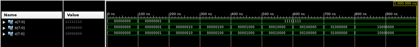
Figure 9 : AND simulations
These two components plus the previous MUX can then be used to implement the ALU, one possible VHDL and Verilog implementation is shown below.
VHDL
----

library IEEE;
use IEEE.STD_LOGIC_1164.ALL;
use IEEE.STD_LOGIC_UNSIGNED.ALL;

entity ALU is
port (
  A, B : in  STD_LOGIC_VECTOR(7 downto 0);
  CTL  : in  STD_LOGIC_VECTOR(2 downto 0);
  Y    : out STD_LOGIC_VECTOR(7 downto 0) );
end ALU;

architecture ALU_ARCH of ALU is

  component ADDSUB_8
  port (
    A, B : in  STD_LOGIC_VECTOR(7 downto 0);
    SEL  : in  STD_LOGIC;
    Y    : out STD_LOGIC_VECTOR(7 downto 0);
    C    : out STD_LOGIC );
  end component;

  component AND_2_8
  port(
    A : IN  STD_LOGIC_VECTOR( 7 downto 0 );
    B : IN  STD_LOGIC_VECTOR( 7 downto 0 );
    Z : OUT STD_LOGIC_VECTOR( 7 downto 0 ) );
  end component;

  component MUX_2_8
  port (
    A, B : in  STD_LOGIC_VECTOR(7 downto 0);
    SEL  : in  STD_LOGIC;
    Y    : out STD_LOGIC_VECTOR(7 downto 0) );
  end component;

  signal mux_int : STD_LOGIC_VECTOR(7 downto 0);
  signal addsub_int : STD_LOGIC_VECTOR(7 downto 0);
  signal and_int : STD_LOGIC_VECTOR(7 downto 0);

  signal carry : STD_LOGIC;

begin

 mux_a : MUX_2_8 port map(
    A   => mux_int,
    B   => B,
    SEL => CTL(2),
    Y   => Y );

 muxb : MUX_2_8 port map(
    A   => addsub_int,
    B   => and_int,
    SEL => CTL(1),
    Y   => mux_int );

  adder : ADDSUB_8 port map(
    A   => A,
    B   => B,
    SEL => CTL(0),
    Y   => addsub_int,
    C   => carry );

  bitwiseAND : AND_2_8 port map(
    A => A,
    B => B,
    Z => and_int );

end ALU_ARCH;

VERILOG
-------

module ALU (
  input [7:0] A,
  input [7:0] B,
  input [2:0] CTL,
  output [7:0] Y );

  wire [7:0] mux_int;
  wire [7:0] addsub_int;
  wire [7:0] and_int;

  MUX_2_8 mux_a (
    .A(mux_int),
    .B(B),
    .SEL(CTL[2]),
    .Y(Y) );

  MUX_2_8 mux_b (
    .A(addsub_int),
    .B(and_int),
    .SEL(CTL[1]),
    .Y(mux_int) );

  ADDSUB_8 add_sub (
    .A(A),
    .B(B),
    .SEL(CTL[0]),
    .Y(addsub_int),
    .C(carry) );

  AND_2_8 bitwiseAND (
    .A(A),
    .B(B),
    .Z(and_int) );

endmodule
You can download copies of these files as a ISE project with testbench here: (Link). Note, the .vhd and .v files need to be manually added to the project one at a time for testing as they use the same name. From these HDL descriptions the Xilinx ISE tools can create an RTL schemtic, as shown in figure 10. A waveform diagram of this component in action is shown in figure 11 below.
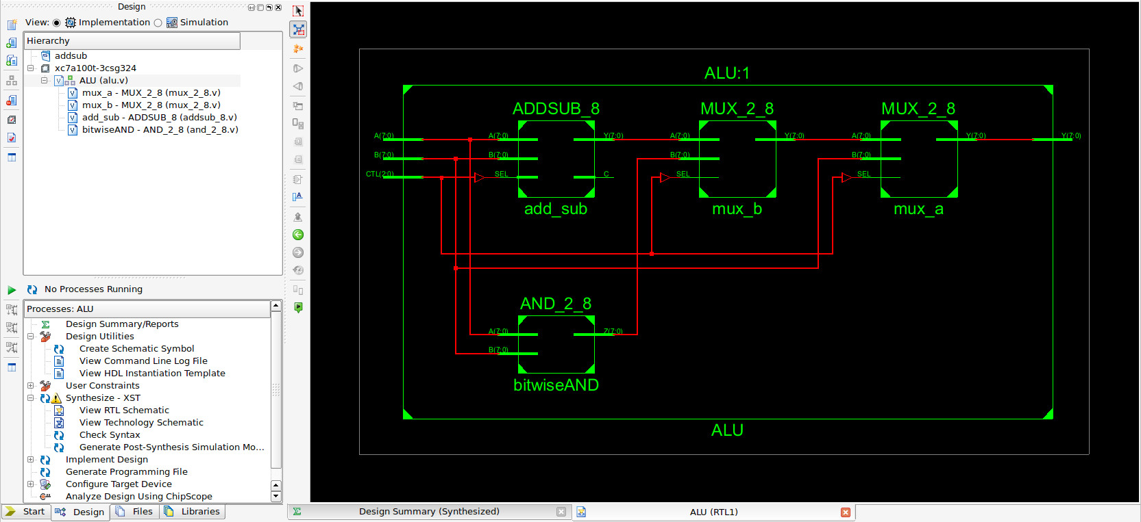
Figure 10 : ALU schematic
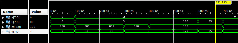
Figure 11 : ALU simulation
Note, ADD="000", SUB="001", AND="010", PASS="100".
Again, i used the same basic architecture as the previous FPGA implementation (Link), building a 4bit register from D-type flip-flops, then using this component to produce the 8bit and 16bit registers. The aim here was to show component reuse and hierarchical design.
VHDL
----

library IEEE;
use IEEE.STD_LOGIC_1164.ALL;

entity REG_4 is
port (
  D   : in STD_LOGIC_VECTOR(3 downto 0);
  Q   : out STD_LOGIC_VECTOR(3 downto 0);
  CLK : in STD_LOGIC;
  CLR : in STD_LOGIC;
  CE  : in STD_LOGIC);
end REG_4;

architecture REG_4_ARCH of REG_4 is
begin

  process (CLK, CLR)
  begin
    if CLR = '1'
    then
      Q <= (others => '0');
    elsif CLK='1' and CLK'event
    then
      if CE = '1'
      then
        Q <= D;
      end if;
    end if;
  end process;

end REG_4_ARCH

VERILOG
-------

module REG_4 ( D, Q, CLK, CLR, CE );
  input [3:0] D;
  input CLK;
  input CLR;
  input CE;
  output reg [3:0] Q;

always @(posedge CLK or posedge CLR)
begin
  if (CLR)
    Q <= 4'b0000;
  else if (CE)
    Q <= D;
end
endmodule
In Verilog the "always" keyword defines a procedural block, the @ symbol is used to define the sensitivity list for the procedural block. A sensitivity list specifies the signals / conditions that should change for that block to be "executed". In VHDL a comparable construct is the PROCESS, its sensitivity list is defined by its ( ). Note, as there is only one assignment in the IF-ELSE structure you do not need to declare a "begin-end" block. A block is only needed if you have multiple assignments. The IF condition statement must be in a ( ), use == for bus, or variable comparisons. This can also be used for bit inputs e.g. CLR and CE, but this not required, see example above. To signal that the Q output is registered you must use the "reg" output type. Default type is wire. Assignments are made using non-blocking assignments "<=".
To construct an 8bit register we can use two REG_4 components, one possible VHDL and Verilog implementation is shown below.
VHDL
----

library IEEE;
use IEEE.STD_LOGIC_1164.ALL;

entity REG_8 is
port (
  D   : in STD_LOGIC_VECTOR(7 downto 0);
  Q   : out STD_LOGIC_VECTOR(7 downto 0);
  CLK : in STD_LOGIC;
  CLR : in STD_LOGIC;
  CE  : in STD_LOGIC );
end REG_8;

architecture REG_8_ARCH of REG_8 is

  component REG_4
  port (
    D   : in STD_LOGIC_VECTOR(3 downto 0);
    Q   : out STD_LOGIC_VECTOR(3 downto 0);
    CLK : in STD_LOGIC;
    CLR : in STD_LOGIC;
    CE  : in STD_LOGIC);
  end component;

begin
  reg_low: REG_4 port map (
    D   => D(3 downto 0),
    Q   => Q(3 downto 0),
    CLK => CLK,
    CLR => CLR,
    CE  => CE );

  reg_high: REG_4 port map (
    D   => D(7 downto 4),
    Q   => Q(7 downto 4),
    CLK => CLK,
    CLR => CLR,
    CE  => CE );

end REG_8_ARCH;

VERILOG
-------

module REG_8 (
  input [7:0] D,
  input CLK,
  input CLR,
  input CE,
  output [7:0] Q );

  REG_4 reg_low (
    .D(D[3:0]),
    .CLK(CLK),
    .CLR(CLR),
    .CE(CE),
    .Q(Q[3:0]) );

  REG_4 reg_high (
    .D(D[7:4]),
    .CLK(CLK),
    .CLR(CLR),
    .CE(CE),
    .Q(Q[7:4]) );

endmodule
In Verilog "." defines a port, the associated "()" defines the wire it is connected to. To construct a 16bit register we can use two REG_8 components, one possible VHDL and Verilog implementation is shown below.
VHDL
----

library IEEE;
use IEEE.STD_LOGIC_1164.ALL;

entity REG_16 is
port (
  D   : in STD_LOGIC_VECTOR(15 downto 0);
  Q   : out STD_LOGIC_VECTOR(15 downto 0);
  CLK : in STD_LOGIC;
  CLR : in STD_LOGIC;
  CE  : in STD_LOGIC );
end REG_16;

architecture REG_16_ARCH of REG_16 is

  component REG_8
  port (
    D   : in STD_LOGIC_VECTOR(7 downto 0);
    Q   : out STD_LOGIC_VECTOR(7 downto 0);
    CLK : in STD_LOGIC;
    CLR : in STD_LOGIC;
    CE  : in STD_LOGIC);
  end component;

begin
  reg_low: REG_8 port map (
    D   => D(7 downto 0),
    Q   => Q(7 downto 0),
    CLK => CLK,
    CLR => CLR,
    CE  => CE );

  reg_high: REG_8 port map (
    D   => D(15 downto 8),
    Q   => Q(15 downto 8),
    CLK => CLK,
    CLR => CLR,
    CE  => CE );

end REG_16_ARCH;

VERILOG
-------

module REG_16 (
  input [15:0] D,
  input CLK,
  input CLR,
  input CE,
  output [15:0] Q );

  REG_8 reg_low (
    .D(D[7:0]),
    .CLK(CLK),
    .CLR(CLR),
    .CE(CE),
    .Q(Q[7:0]) );

  REG_8 reg_high (
    .D(D[15:8]),
    .CLK(CLK),
    .CLR(CLR),
    .CE(CE),
    .Q(Q[15:8]) );

endmodule
You can download copies of these files as a ISE project with testbench here: (Link). Note, the .vhd and .v files need to be manually added to the project one at a time for testing as they use the same name. From these HDL descriptions the Xilinx ISE tools can create an RTL schemtic, as shown in figure 12. A waveform diagram of this component in action is shown in figure 13 below.
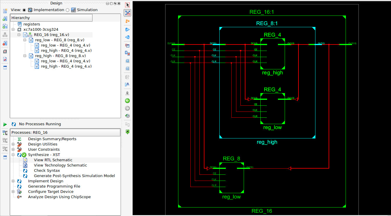
Figure 12 : REG_16 schematic
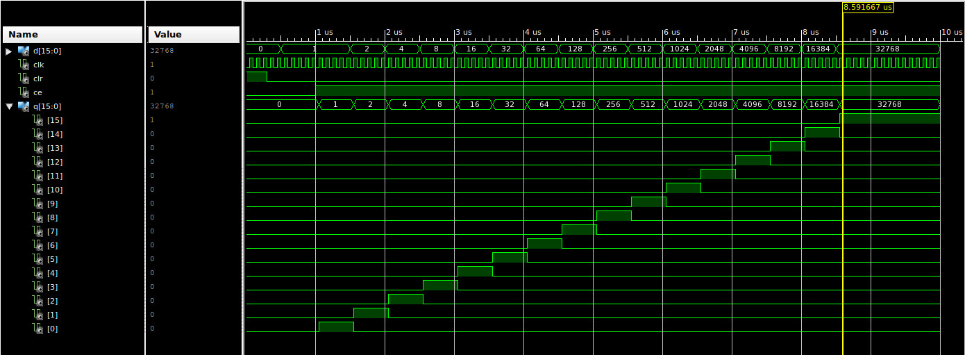
Figure 13 : REG_16 simulation
The program counter (PC) and the ring-counter, are also base on the same designs as the FPGA implementation (Link), however, i decided to build these using behavioural descriptions, one possible VHDL and Verilog implementation of a ring counter is shown below.
VHDL
----

library IEEE;
use IEEE.STD_LOGIC_1164.ALL;
use IEEE.STD_LOGIC_UNSIGNED.ALL;

entity RING_COUNTER_3 is
port (
  CLK : in STD_LOGIC;
  RST : in STD_LOGIC;
  Q   : out STD_LOGIC_VECTOR(2 downto 0));
end RING_COUNTER_3;

architecture RING_COUNTER_3_ARCH of RING_COUNTER_3 is
  signal q_int : STD_LOGIC_VECTOR(2 downto 0);
begin
  process (CLK, RST)
  begin
    if RST = '1'
    then
      q_int <= "001";
    elsif CLK='1' and CLK'event
    then
      q_int <= q_int(1 downto 0) & q_int(2);
    end if;
  end process;

  Q <= q_int;

end RING_COUNTER_3_ARCH;

VERILOG
-------

module RING_COUNTER_3 (
  input wire CLK,
  input wire RST,
  output reg [2:0] Q );

always @(posedge CLK or posedge RST) begin
  if (RST)
    Q <= 3'b001;
  else
    Q <= {Q[1:0], Q[2]};
end
endmodule
From these HDL descriptions the Xilinx ISE tools can create an RTL schemtic, as shown in figure 14. A waveform diagram of this component in action is shown in figure 15 below.
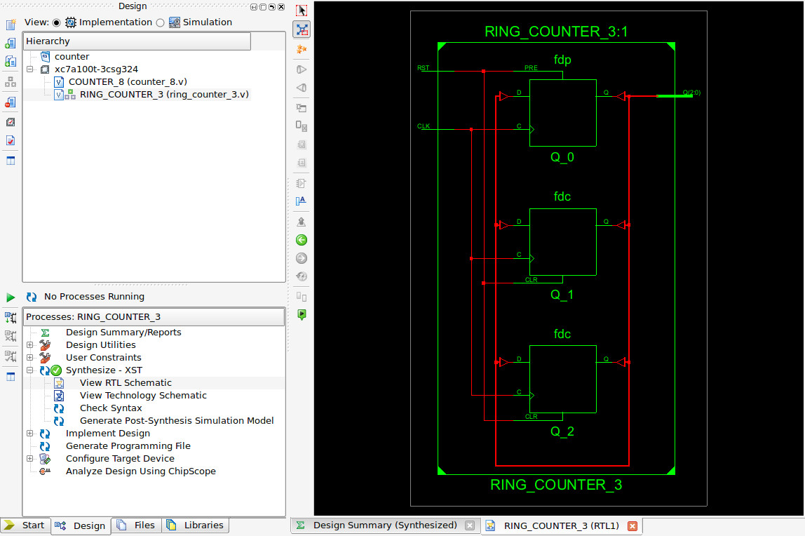
Figure 14 : RING_COUNTER_3 schematic
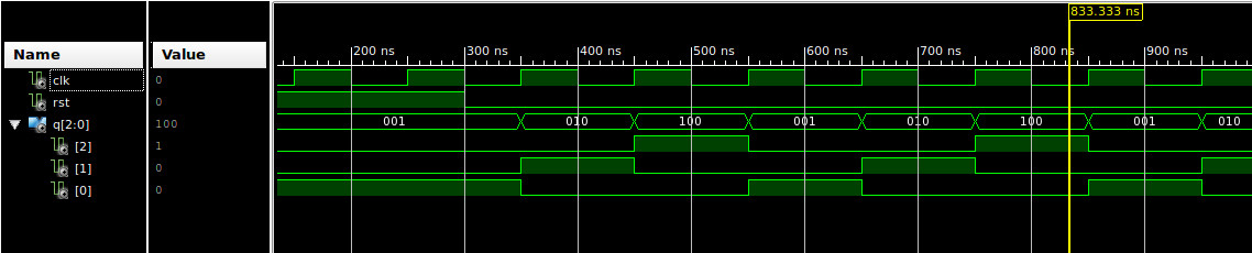
Figure 15 : RING_COUNTER_3 simulation
One possible VHDL and Verilog implementation of a loadable binary counter is shown below.
VHDL
----

library IEEE;
use IEEE.STD_LOGIC_1164.ALL;
use IEEE.STD_LOGIC_UNSIGNED.ALL;

entity COUNTER_8 is
Port (
  CLK : in  STD_LOGIC;
  CLR : in  STD_LOGIC;
  LD  : in  STD_LOGIC;
  CE  : in  STD_LOGIC;
  D   : in  STD_LOGIC_VECTOR(7 downto 0);
  Q   : out STD_LOGIC_VECTOR(7 downto 0) );
end COUNTER_8;

architecture COUNTER_8_ARCH of COUNTER_8 is
  signal q_int : STD_LOGIC_VECTOR(7 downto 0) := (others => '0');
begin

  process (CLK, CLR)
  begin
    if CLR='1'
    then
      q_int <= (others => '0');
    elsif CLK='1' and CLK'event
    then
      if CE='1'
      then
        if LD='1'
        then
          q_int <= D;
        else
          q_int <= q_int + 1;
        end if;
      end if;
    end if;
  end process;

  Q <= q_int;

end COUNTER_8_ARCH;

VERILOG
-------

module COUNTER_8 (
  input wire CLK,
  input wire CLR,
  input wire LD,
  input wire CE,
  input wire [7:0] D,
  output reg [7:0] Q );

always @(posedge CLK or posedge CLR) begin
  if (CLR)
    Q <= 8'b00000000;
  else if (CE)
    if (LD)
      Q <= D;
    else
      Q <= Q + 1;
end

endmodule
A difference between VHDL and Verilog is that a process in VHDL can not be read an output port as its an output i.e. you can only read inputs, therefore you need an internal signal as a temp buffer. In VHDL this is represented using the signal "q_int". You can download copies of these files as a ISE project with testbench here: (Link). Note, the .vhd and .v files need to be manually added to the project one at a time for testing as they use the same name. From these HDL descriptions the Xilinx ISE tools can create an RTL schemtic, as shown in figure 16. A waveform diagram of this component in action is shown in figure 17 below.
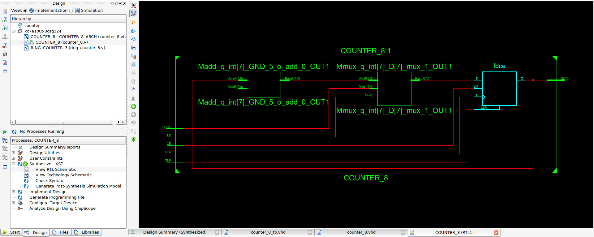
Figure 16 : COUNTER_8 schematic
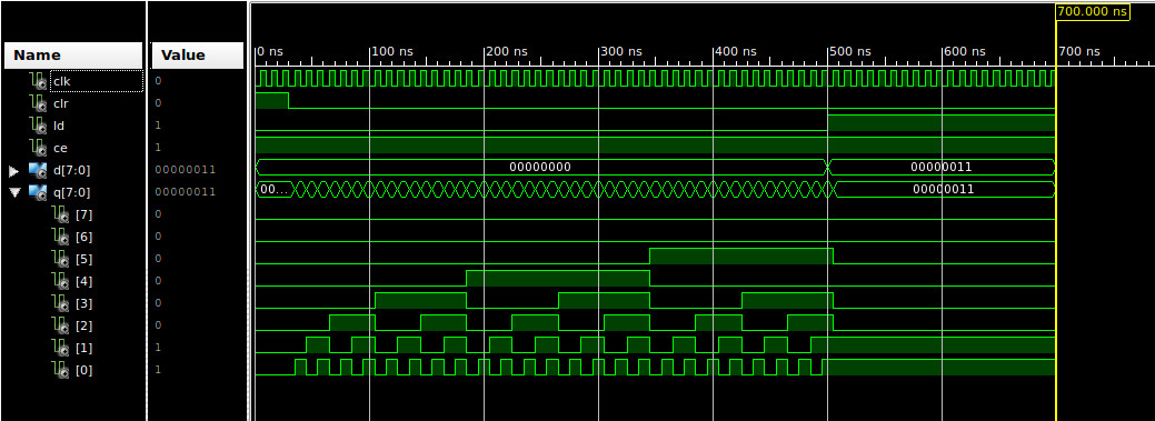
Figure 17 : COUNTER_8 simulation
The control logic is the same as used by the Logisim implementation (Link) A key component is a 4bit onehot decoder, one possible VHDL and Verilog implementation is shown below.
VHDL
----

library IEEE;
use IEEE.STD_LOGIC_1164.ALL;

entity ONEHOT_DECODER_16 is
port (
  A : in  STD_LOGIC_VECTOR(3 downto 0);
  Y : out STD_LOGIC_VECTOR(15 downto 0) );
end ONEHOT_DECODER_16;

architecture ONEHOT_DECODER_16_ARCH of ONEHOT_DECODER_16 is
begin
  process (A)
  begin
    case A is
      when "0000" => Y <= "0000000000000001";
      when "0001" => Y <= "0000000000000010";
      when "0010" => Y <= "0000000000000100";
      when "0011" => Y <= "0000000000001000";
      when "0100" => Y <= "0000000000010000";
      when "0101" => Y <= "0000000000100000";
      when "0110" => Y <= "0000000001000000";
      when "0111" => Y <= "0000000010000000";
      when "1000" => Y <= "0000000100000000";
      when "1001" => Y <= "0000001000000000";
      when "1010" => Y <= "0000010000000000";
      when "1011" => Y <= "0000100000000000";
      when "1100" => Y <= "0001000000000000";
      when "1101" => Y <= "0010000000000000";
      when "1110" => Y <= "0100000000000000";
      when "1111" => Y <= "1000000000000000";
      when OTHERS => Y <= (OTHERS => '0');
    end case;
  end process;
end ONEHOT_DECODER_16_ARCH;

VERILOG
-------

module ONEHOT_DECODER_16 (
  input  wire [3:0] A,
  output reg [15:0] Y );

always @(*) begin
  case (A)
    4'b0000: Y = 16'b0000000000000001;
    4'b0001: Y = 16'b0000000000000010;
    4'b0010: Y = 16'b0000000000000100;
    4'b0011: Y = 16'b0000000000001000;
    4'b0100: Y = 16'b0000000000010000;
    4'b0101: Y = 16'b0000000000100000;
    4'b0110: Y = 16'b0000000001000000;
    4'b0111: Y = 16'b0000000010000000;
    4'b1000: Y = 16'b0000000100000000;
    4'b1001: Y = 16'b0000001000000000;
    4'b1010: Y = 16'b0000010000000000;
    4'b1011: Y = 16'b0000100000000000;
    4'b1100: Y = 16'b0001000000000000;
    4'b1101: Y = 16'b0010000000000000;
    4'b1110: Y = 16'b0100000000000000;
    4'b1111: Y = 16'b1000000000000000;
    default: Y = 16'b0000000000000000;
  endcase
end

endmodule
Personally i find the way verilog defines stuff a little odd. In this example the output Y is declared as "reg" because it’s being assigned inside the always block. However, since the block is combinatorial (always @(*)), rather than clocked (@(posedge clk or rst)) the synthesized hardware will be combinational, not sequential. If you don't use "reg" you will get a compilation error. This feels odd, the "reg" keyword is used to declare variables that can hold values, not necessarily that these signals are registered i.e. driven by flip-flops. Also not sure about how constants / binary strings are declared i.e. size'bvalue, hmmm. From these HDL descriptions the Xilinx ISE tools can create an RTL schemtic, as shown in figure 18. A waveform diagram of this component in action is shown in figure 19 below.
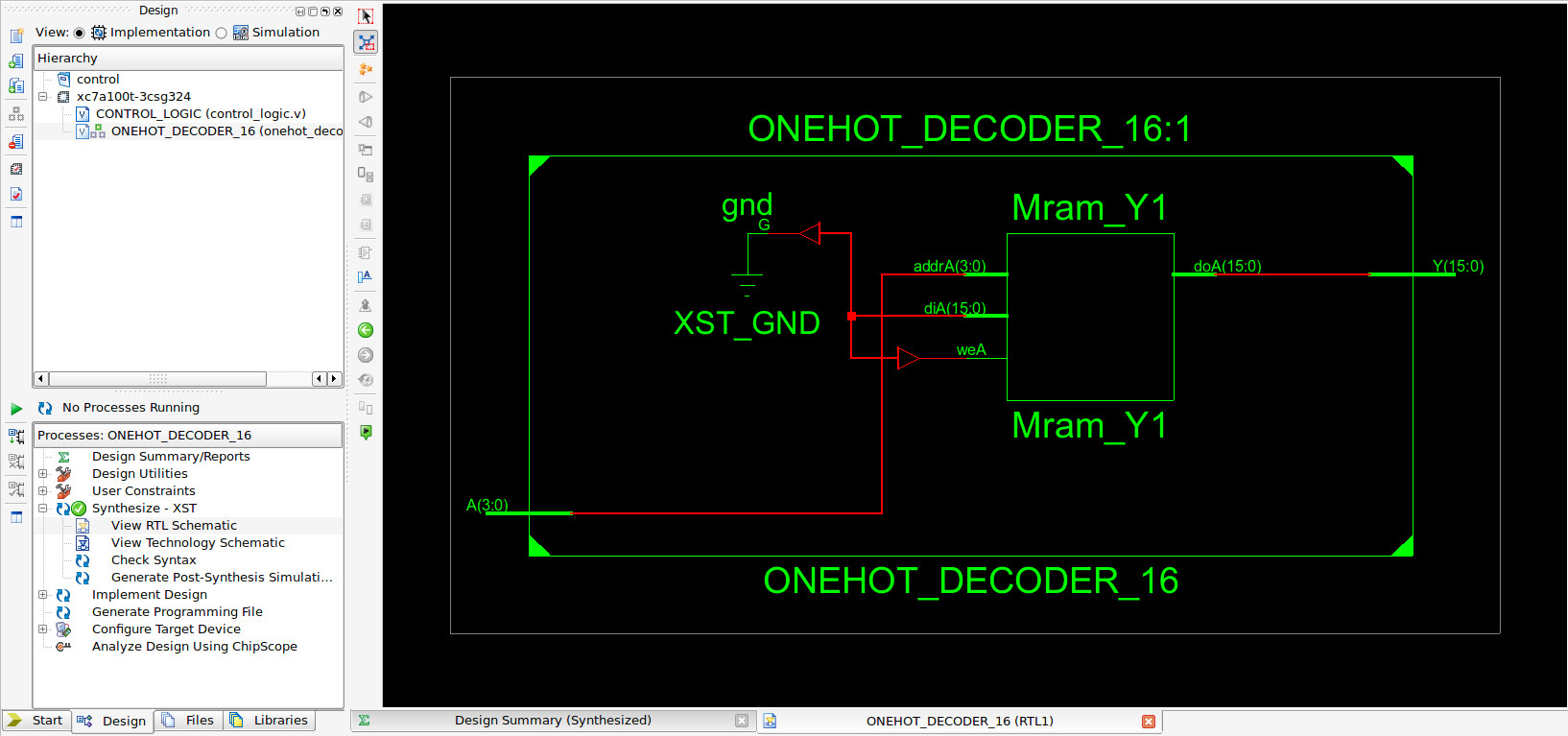
Figure 18 : ONEHOT_DECODER_16 schematic
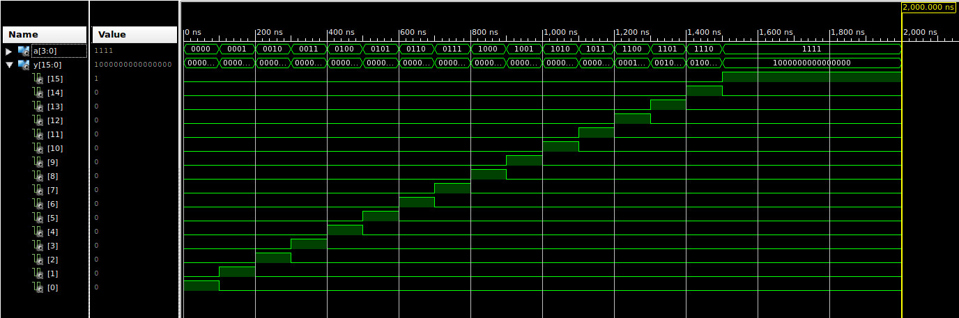
Figure 19 : ONEHOT_DECODER_16 simulation
In addition to a bin-to-onehot decoder the control logic also contains the logic needed to produce the required control signals. Again, these are taken from the original designs, but now implemented using HDLs, one possible VHDL and Verilog implementation is shown below.
VHDL
----

library IEEE;
use IEEE.STD_LOGIC_1164.ALL;

entity DECODER is
port (
  FETCH       : in  STD_LOGIC;
  DECODE      : in  STD_LOGIC;
  EXECUTE     : in  STD_LOGIC;
  MOVE        : in  STD_LOGIC;
  ADD         : in  STD_LOGIC;
  SUB         : in  STD_LOGIC;
  BITWISE_AND : in  STD_LOGIC;
  LOAD        : in  STD_LOGIC;
  ADDM        : in  STD_LOGIC;
  SUBM        : in  STD_LOGIC;
  STORE       : in  STD_LOGIC;
  JUMPU       : in  STD_LOGIC;
  JUMPZ       : in  STD_LOGIC;
  JUMPNZ      : in  STD_LOGIC;
  Z           : in  STD_LOGIC;
  ROM_EN      : OUT STD_LOGIC;
  RAM_EN      : OUT STD_LOGIC;
  RAM_WR      : OUT STD_LOGIC;
  ADDR_SEL    : OUT STD_LOGIC;
  DATA_SEL    : OUT STD_LOGIC;
  ALU_CTL0    : OUT STD_LOGIC;
  ALU_CTL1    : OUT STD_LOGIC;
  ALU_CTL2    : OUT STD_LOGIC;
  ACC_EN      : OUT STD_LOGIC;
  IR_EN       : OUT STD_LOGIC;
  PC_LD       : OUT STD_LOGIC;
  PC_EN       : OUT STD_LOGIC );
end DECODER;

architecture DECODER_ARCH of DECODER is
begin
  process ( FETCH, DECODE, EXECUTE,
            MOVE, ADD, SUB, BITWISE_AND,
            LOAD, ADDM, SUBM, STORE,
            JUMPU, JUMPZ, JUMPNZ, Z )
  begin

    ROM_EN   <= FETCH;
    RAM_EN   <= (DECODE or EXECUTE) and (LOAD or STORE or ADDM or SUBM);
    RAM_WR   <= EXECUTE and STORE;
    ADDR_SEL <= (DECODE or EXECUTE) and (LOAD or STORE or ADDM or SUBM);
    DATA_SEL <= LOAD or ADDM or SUBM;
    ALU_CTL0 <= SUB or SUBM;
    ALU_CTL1 <= BITWISE_AND;
    ALU_CTL2 <= MOVE or LOAD;
    ACC_EN   <= (MOVE or ADD or SUB or BITWISE_AND or LOAD or ADDM or SUBM) and EXECUTE;
    IR_EN    <= FETCH;
    PC_LD    <= DECODE and (JUMPU or (JUMPZ and Z) or (JUMPNZ and not Z));
    PC_EN    <= DECODE;

  end process;
end DECODER_ARCH;

VERILOG
-------

module DECODER (
  input  wire FETCH,
  input  wire DECODE,
  input  wire EXECUTE,
  input  wire MOVE,
  input  wire ADD,
  input  wire SUB,
  input  wire BITWISE_AND,
  input  wire LOAD,
  input  wire ADDM,
  input  wire SUBM,
  input  wire STORE,
  input  wire JUMPU,
  input  wire JUMPZ,
  input  wire JUMPNZ,
  input  wire Z,
  output wire ROM_EN,
  output wire RAM_EN,
  output wire RAM_WR,
  output wire ADDR_SEL,
  output wire DATA_SEL,
  output wire ALU_CTL0,
  output wire ALU_CTL1,
  output wire ALU_CTL2,
  output wire ACC_EN,
  output wire IR_EN,
  output wire PC_LD,
  output wire PC_EN );

  assign ROM_EN   = FETCH;
  assign RAM_EN   = (DECODE | EXECUTE) & (LOAD | STORE | ADDM | SUMB);
  assign RAM_WR   = EXECUTE & STORE;
  assign ADDR_SEL = (DECODE | EXECUTE) & (LOAD | STORE | ADDM | SUBM);
  assign DATA_SEL = LOAD | ADDM | SUBM;
  assign ALU_CTL0 = SUB | SUBM;
  assign ALU_CTL1 = BITWISE_AND;
  assign ALU_CTL2 = MOVE | LOAD;
  assign ACC_EN   = (MOVE | ADD | SUB | BITWISE_AND | LOAD | ADDM | SUBM) & EXECUTE;
  assign IR_EN    = FETCH;
  assign PC_LD    = DECODE & (JUMPU | (JUMPZ & Z) | (JUMPNZ & ~Z));
  assign PC_EN    = DECODE;

endmodule
From these HDL descriptions the Xilinx ISE tools can create an RTL schematic, as shown in figure 20. To fully test this logic would be tricky, so i didn't :). You can download copies of these files as a ISE project with testbench here: (Link). Note, the .vhd and .v files need to be manually added to the project one at a time for testing as they use the same name. For the moment i just constructed a testbench that applied a constant logic-0 on each input, to confirm that there were not syntax errors, that all outputs also produced a logic-0. The final testing of this circuit will be done when it is integrated into the final processor i.e. tested through the execution of the test program.
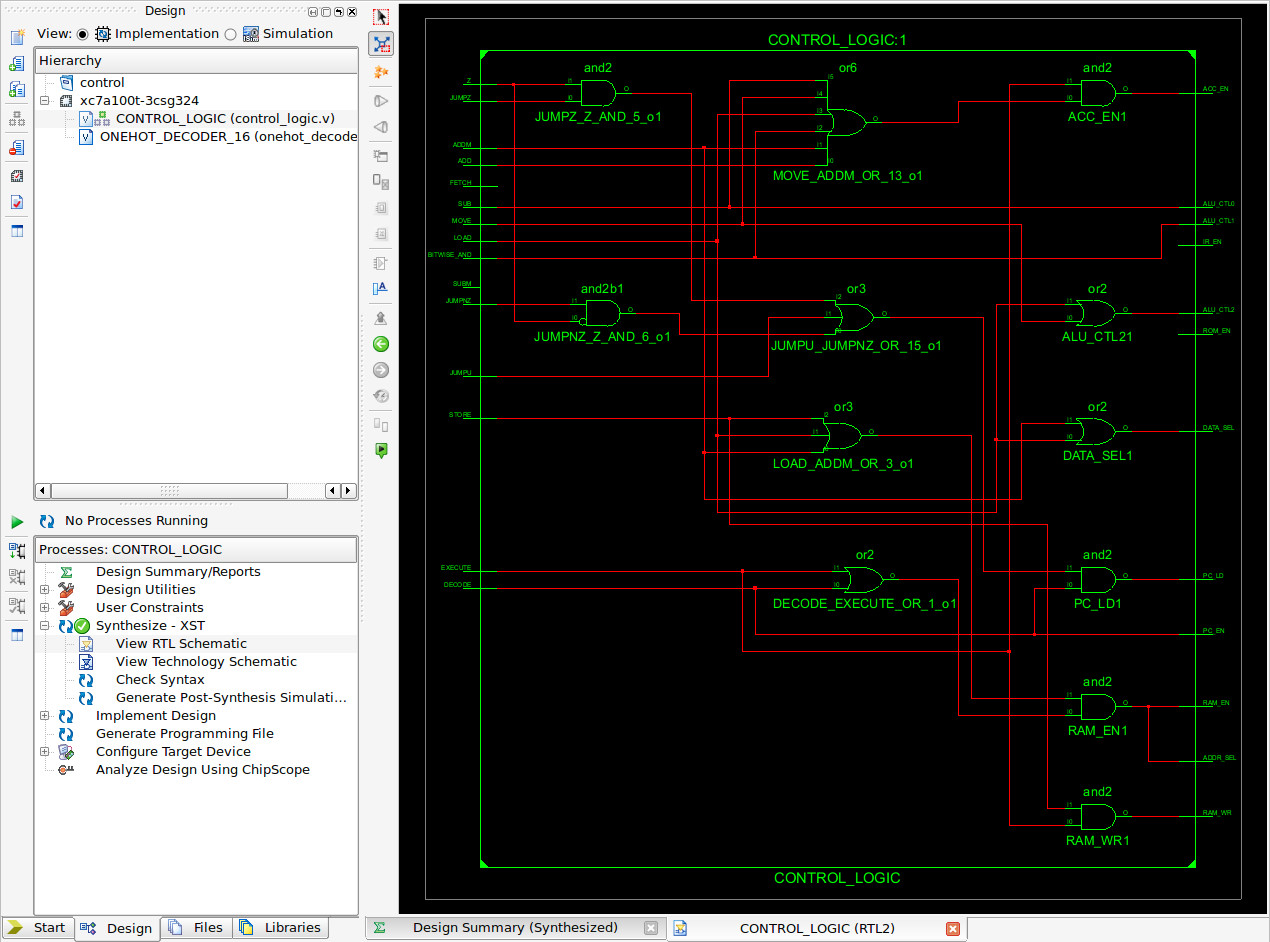
Figure 20 : DECODER schematic
Figure 21 : DECODER simulation
From one point of view memory is just an array and lucky both VHDL and Verilog support this data type, one possible VHDL and Verilog implementation is shown below. Next, its just a question of how do we initialise this array with the required machine code and data.
VHDL
----

library IEEE;
use IEEE.STD_LOGIC_1164.ALL;
use IEEE.NUMERIC_STD.ALL;

entity RAM is
port (
  CLK  : in  STD_LOGIC;
  WE   : in  STD_LOGIC;
  ADDR : in  STD_LOGIC_VECTOR(7 downto 0);
  DIN  : in  STD_LOGIC_VECTOR(15 downto 0);
  DOUT : out STD_LOGIC_VECTOR(15 downto 0) );
end RAM;

architecture RAM_ARCH of RAM is
  type memory_type is array (0 to 2**8) of STD_LOGIC_VECTOR(15 downto 0);
  signal memory : memory_type := (
    0 => x"FFFF",
    OTHERS => (OTHERS => '0'));
begin
  process (clk)
  begin
    if CLK='1' and CLK'event
    then
      if WE = '1'
      then
        memory(to_integer(unsigned(ADDR))) <= DIN;
      end if;
      DOUT <= memory(to_integer(unsigned(ADDR)));
    end if;
  end process;
end RAM_ARCH;

VERILOG
-------
module RAM (
  input wire CLK,
  input wire WE,
  input wire [7:0] ADDR,
  input wire [15:0] DIN,
  output reg [15:0] DOUT );

  reg [7:0] memory [0:255];

  initial
    begin
      memory[0] = 16'hFFFF;
    end

  always @(posedge CLK)
    begin
      if (WE)
        memory[ADDR] <= DIN;
      DOUT <= memory[ADDR]; // Read from memory
    end

endmodule
You can download copies of these files as a ISE project with testbench here: (Link). Note, the .vhd and .v files need to be manually added to the project one at a time for testing as they use the same name. From these HDL descriptions the Xilinx ISE tools can create an RTL schemtic, as shown in figure 22. Hmmmmm, not sure why this produced a registered output, will double check what primitives this was built from i.e. LUT or BlockRAM memory? However, should be fine for simulations. Again, going to test these implementations using the processor running the test program.
Figure 22 : RAM schematic
To load the required machine-code and data into these memory components i decided to go simple and manually cut and paste i.e. write a Bash script to convert the assemblers object files into the required VHDL: 0 => x"FFFF" and Verilog memory[0] = 16'hFFFF; assignments needed for each memory location.
VHDL
----
#!/bin/sh

echo -n > vhdlData
cat code.dat | while read line
do
  addr=`echo $line | cut -d' ' -f1`
  data=`echo $line | cut -d' ' -f2`
  echo "    $addr => \"$data\"," >> vhdlData
done

VERILOG
-------
#!/bin/sh

echo -n > verilogData
cat code.dat | while read line
do
  addr=`echo $line | cut -d' ' -f1`
  data=`echo $line | cut -d' ' -f2`
  echo "      "memory[$addr] = "16'b"$data";" >> verilogData
done
To test these RAM models i used the normal test code as shown below. This was assembled using the python based assembler to produce the code.dat object file, this is then converted into the required data value using the above scripts, you can download these here: Link.
###################
# INSTRUCTION-SET #
###################

# INSTR   IR15 IR14 IR13 IR12 IR11 IR10 IR09 IR08 IR07 IR06 IR05 IR04 IR03 IR02 IR01 IR00
# MOVE    0    0    0    0    X    X    X    X    K    K    K    K    K    K    K    K
# ADD     0    0    0    1    X    X    X    X    K    K    K    K    K    K    K    K
# SUB     0    0    1    0    X    X    X    X    K    K    K    K    K    K    K    K
# AND     0    0    1    1    X    X    X    X    K    K    K    K    K    K    K    K

# LOAD    0    1    0    0    X    X    X    X    A    A    A    A    A    A    A    A
# STORE   0    1    0    1    X    X    X    X    A    A    A    A    A    A    A    A
# ADDM    0    1    1    0    X    X    X    X    A    A    A    A    A    A    A    A
# SUBM    0    1    1    1    X    X    X    X    A    A    A    A    A    A    A    A

# JUMPU   1    0    0    0    X    X    X    X    A    A    A    A    A    A    A    A
# JUMPZ   1    0    0    1    X    X    X    X    A    A    A    A    A    A    A    A
# JUMPNZ  1    0    1    0    X    X    X    X    A    A    A    A    A    A    A    A
# JUMPC   1    0    1    1    X    X    X    X    A    A    A    A    A    A    A    A        -- NOT IMPLEMENTED

########
# CODE #
########

start:
  move 1            # acc = 1
  move 3            # acc = 3
  move 7            # acc = 7
  move 15           # acc = 15    F
  move 31           # acc = 31   1F
  move 63           # acc = 63   3F
  move 127          # acc = 127  7F
  move 255          # acc = 255  FF

  add 1             # acc = 0     0
  add 3             # acc = 3     3
  add 7             # acc = 10    A
  add 15            # acc = 25   19
  add 31            # acc = 56   38
  add 63            # acc = 119  77
  add 127           # acc = 246  F6
  add 255           # acc = 245  F5

  sub 1             # acc = 244  F4
  sub 3             # acc = 241  F1
  sub 7             # acc = 234  EA
  sub 15            # acc = 219  DB
  sub 31            # acc = 188  BC
  sub 63            # acc = 125  7D
  sub 127           # acc = 254  FE
  sub 255           # acc = 255  FF

  and 255           # acc = 255  FF
  and 127           # acc = 127  7F
  and 63            # acc = 63   3F
  and 31            # acc = 31   1F
  and 15            # acc = 15    F
  and 7             # acc = 7     7
  and 3             # acc = 3     3
  and 1             # acc = 1     1

  move 1            # acc = 1     1
  store A           # M[87] = 1
  move 3            # acc = 3     3
  store B           # M[88] = 3
  move 7            # acc = 7     7
  store C           # M[89] = 7
  move 15           # acc = 15    F
  store D           # M[90] = 15
  move 31           # acc = 31    1F
  store E           # M[91] = 31
  move 63           # acc = 63    3F
  store F           # M[92] = 63
  move 127          # acc = 127   7F
  store G           # M[93] = 127
  move 255          # acc = 255   FF
  store H           # M[94] = 255

  load A            # acc = M[87] = 1     1
  load B            # acc = M[88] = 3     3
  load C            # acc = M[89] = 7     7
  load D            # acc = M[90] = 15    F
  load E            # acc = M[91] = 31   1F
  load F            # acc = M[92] = 63   3F
  load G            # acc = M[93] = 127  7F
  load H            # acc = M[94] = 255  FF

  addm A            # acc = 0     0
  addm B            # acc = 3     3
  addm C            # acc = 10    A
  addm D            # acc = 25   19
  addm E            # acc = 56   38
  addm F            # acc = 119  77
  addm G            # acc = 246  F6
  addm H            # acc = 245  F5

  subm A            # acc = 244  F4
  subm B            # acc = 241  F1
  subm C            # acc = 234  EA
  subm D            # acc = 219  DB
  subm E            # acc = 188  BC
  subm F            # acc = 125  7D
  subm G            # acc = 254  FE
  subm H            # acc = 255  FF

  and 0             # acc = 0
  jumpz b1          # TAKEN
  move 255          # set acc to 255 if error

b1:
  add 1             # acc = 1
  jumpnz b2         # TAKEN
  move 255          # set acc to 255 if error

b2:
  and 0             # acc = 0
  jumpnz b3         # FALSE
  jumpu b4          # unconditional jump
b3:
  move 255          # set acc to 255 if error

b4:
  add 1             # acc = 1
  jumpz b5          # FALSE
  jumpu b6          # unconditional jump
b5:
  move 255          # set acc to 255 if error

b6:
  jumpu start       # jump back to start

A:
  .data 0
B:
  .data 0
C:
  .data 0
D:
  .data 0
E:
  .data 0
F:
  .data 0
G:
  .data 0
H:
  .data 0
The final simpleCPU implementations are shown in figures 23 and 24. A simulation of this processor running the tested program is shown in figure 25. You can download copies of these files as a ISE project with testbench here: (Link), (Link). Note, the .vhd and .v files need to be manually added to the project one at a time for testing as they use the same name.
Figure 23 : simpleCPU verilog schematic
Figure 24 : simpleCPU vhdl schematic
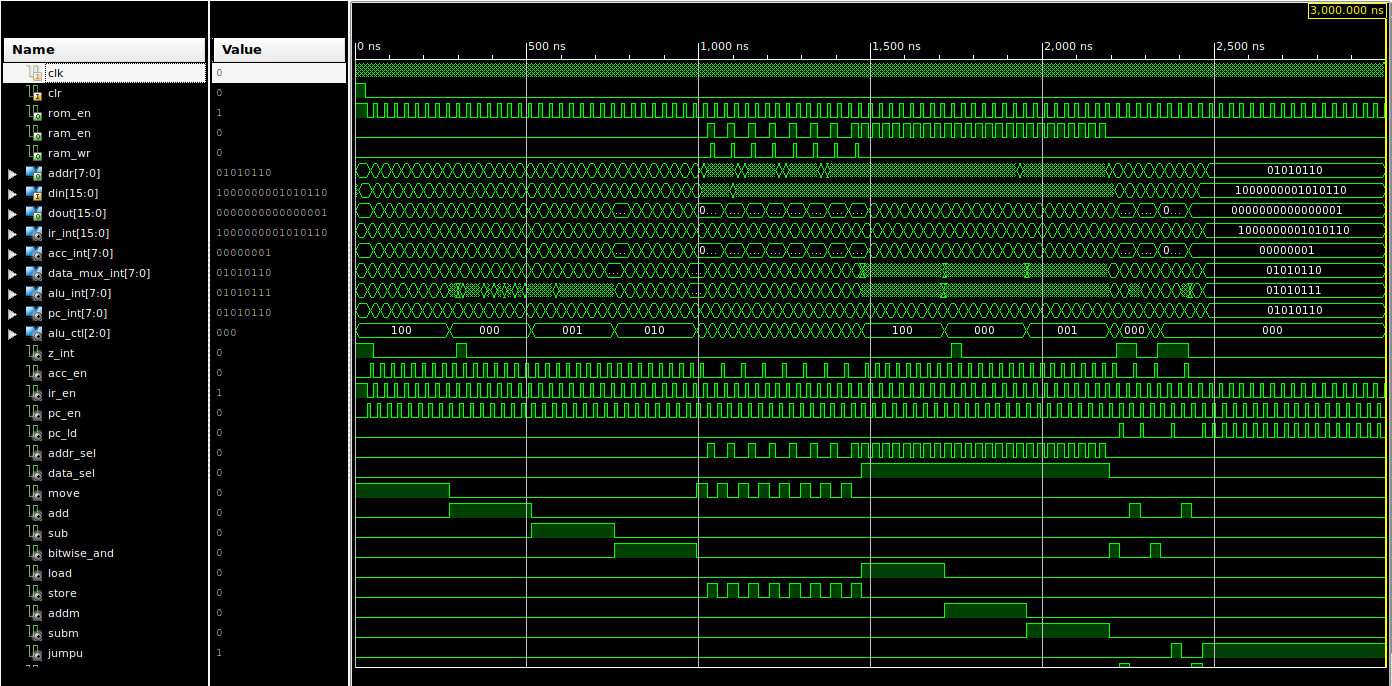
Figure 25 : simpleCPU simulation
To confirm that this simulation is working correctly you can do a visual inspection, but its quicker just to print changes to the DATA_OUT bus to the screen. This is easy to do in the VHDL testbench. A public confession, in the past i remember writing a function to convert STD_LOGIC_VECTOR to a HEX string, but the thought searching through a lot of old backups was a little depressing, so to my shame i used copilot, which gave me:
function to_hex_string(vec: std_logic_vector) return string is
  variable hex_string : string(1 to (vec'length / 4));
  variable nibble     : std_logic_vector(3 downto 0);
begin
  for i in 0 to (vec'length / 4 - 1) loop
    nibble := vec(vec'length - 1 - i * 4 downto vec'length - 4 - i * 4);
    case nibble is
      when "0000" => hex_string(i + 1) := '0';
      when "0001" => hex_string(i + 1) := '1';
      when "0010" => hex_string(i + 1) := '2';
      when "0011" => hex_string(i + 1) := '3';
      when "0100" => hex_string(i + 1) := '4';
      when "0101" => hex_string(i + 1) := '5';
      when "0110" => hex_string(i + 1) := '6';
      when "0111" => hex_string(i + 1) := '7';
      when "1000" => hex_string(i + 1) := '8';
      when "1001" => hex_string(i + 1) := '9';
      when "1010" => hex_string(i + 1) := 'A';
      when "1011" => hex_string(i + 1) := 'B';
      when "1100" => hex_string(i + 1) := 'C';
      when "1101" => hex_string(i + 1) := 'D';
      when "1110" => hex_string(i + 1) := 'E';
      when "1111" => hex_string(i + 1) := 'F';
      when others => hex_string(i + 1) := 'X';
    end case;
  end loop;
  return hex_string;
end to_hex_string;
This function can then be used in the PROCESS below, within the testbench:
debug: process
  variable data : line;
begin
  wait until DOUT'event;

  write(data, now);
  write(data, string'(" : DOUT = "));
  write(data, DOUT);
  write(data, string'(" = "));
  write(data, to_hex_string(DOUT));
  writeline(output, data);
end process;
This process prints to the screen the time, binary value and hex value of the DOUT_BUS each time it changes, as shown below:.
0 ns   : DOUT = 00000000UUUUUUUU = 00XX
0 ns   : DOUT = 0000000000000000 = 0000
55 ns  : DOUT = 0000000000000001 = 0001
85 ns  : DOUT = 0000000000000011 = 0003
115 ns : DOUT = 0000000000000111 = 0007
145 ns : DOUT = 0000000000001111 = 000F
175 ns : DOUT = 0000000000011111 = 001F
205 ns : DOUT = 0000000000111111 = 003F
235 ns : DOUT = 0000000001111111 = 007F
265 ns : DOUT = 0000000011111111 = 00FF
295 ns : DOUT = 0000000000000000 = 0000
325 ns : DOUT = 0000000000000011 = 0003
355 ns : DOUT = 0000000000001010 = 000A
385 ns : DOUT = 0000000000011001 = 0019
415 ns : DOUT = 0000000000111000 = 0038
445 ns : DOUT = 0000000001110111 = 0077
475 ns : DOUT = 0000000011110110 = 00F6
505 ns : DOUT = 0000000011110101 = 00F5
535 ns : DOUT = 0000000011110100 = 00F4
565 ns : DOUT = 0000000011110001 = 00F1
595 ns : DOUT = 0000000011101010 = 00EA
625 ns : DOUT = 0000000011011011 = 00DB
655 ns : DOUT = 0000000010111100 = 00BC
685 ns : DOUT = 0000000001111101 = 007D
715 ns : DOUT = 0000000011111110 = 00FE
745 ns : DOUT = 0000000011111111 = 00FF
805 ns : DOUT = 0000000001111111 = 007F
835 ns : DOUT = 0000000000111111 = 003F
865 ns : DOUT = 0000000000011111 = 001F
895 ns : DOUT = 0000000000001111 = 000F
925 ns : DOUT = 0000000000000111 = 0007
955 ns : DOUT = 0000000000000011 = 0003
985 ns : DOUT = 0000000000000001 = 0001
ISim>
# run 1.00us
1075 ns : DOUT = 0000000000000011 = 0003
1135 ns : DOUT = 0000000000000111 = 0007
1195 ns : DOUT = 0000000000001111 = 000F
1255 ns : DOUT = 0000000000011111 = 001F
1315 ns : DOUT = 0000000000111111 = 003F
1375 ns : DOUT = 0000000001111111 = 007F
1435 ns : DOUT = 0000000011111111 = 00FF
1495 ns : DOUT = 0000000000000001 = 0001
1525 ns : DOUT = 0000000000000011 = 0003
1555 ns : DOUT = 0000000000000111 = 0007
1585 ns : DOUT = 0000000000001111 = 000F
1615 ns : DOUT = 0000000000011111 = 001F
1645 ns : DOUT = 0000000000111111 = 003F
1675 ns : DOUT = 0000000001111111 = 007F
1705 ns : DOUT = 0000000011111111 = 00FF
1735 ns : DOUT = 0000000000000000 = 0000
1765 ns : DOUT = 0000000000000011 = 0003
1795 ns : DOUT = 0000000000001010 = 000A
1825 ns : DOUT = 0000000000011001 = 0019
1855 ns : DOUT = 0000000000111000 = 0038
1885 ns : DOUT = 0000000001110111 = 0077
1915 ns : DOUT = 0000000011110110 = 00F6
1945 ns : DOUT = 0000000011110101 = 00F5
1975 ns : DOUT = 0000000011110100 = 00F4
ISim>
# run 1.00us
2005 ns : DOUT = 0000000011110001 = 00F1
2035 ns : DOUT = 0000000011101010 = 00EA
2065 ns : DOUT = 0000000011011011 = 00DB
2095 ns : DOUT = 0000000010111100 = 00BC
2125 ns : DOUT = 0000000001111101 = 007D
2155 ns : DOUT = 0000000011111110 = 00FE
2185 ns : DOUT = 0000000011111111 = 00FF
2215 ns : DOUT = 0000000000000000 = 0000
2275 ns : DOUT = 0000000000000001 = 0001
2335 ns : DOUT = 0000000000000000 = 0000
2425 ns : DOUT = 0000000000000001 = 0001
ISim>
This can then be compared to the expected ACC value shown in the test program comments. Doing this i did discover some errors in the control logic, but i went back and corrected these, so job done maybe?
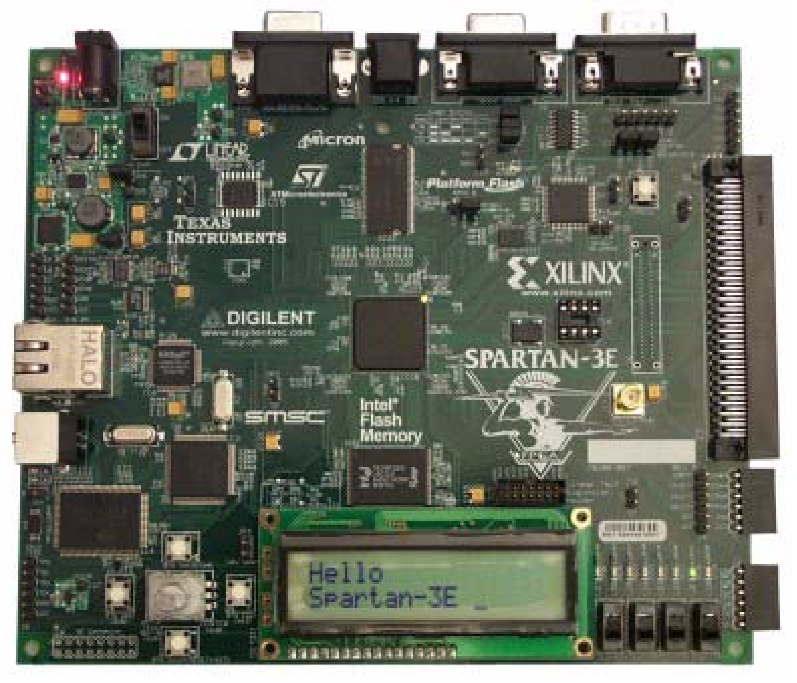
Figure 26 : FPGA Board
As always the only true test to see if something works is to build it, in this case to implement these HDL versions of the processor on an FPGA. The FPGA chosen was an old Spartan 3E board, as shown in figure 26, no good reason to select this board except that i had one on my desk :). To test out this processor we need to add some General Purpose Input Output (GPIO), some means for the processor to interact with the outside world, something we can connect a scope to. One possible VHDL implementation is shown below:
Note, we do also need to add some other system stuff as well e.g. reset and clock components, we will look at these later.
library IEEE;
use IEEE.STD_LOGIC_1164.ALL;

entity GPIO_8 is
port (
  CLK  : in  STD_LOGIC;
  CLR  : in  STD_LOGIC;
  WE   : in  STD_LOGIC;
  CE   : in  STD_LOGIC;
  ADDR : in  STD_LOGIC;
  DIN  : in  STD_LOGIC_VECTOR(15 downto 0);
  DOUT : out STD_LOGIC_VECTOR(15 downto 0);
  GPI  : in  STD_LOGIC_VECTOR(7 downto 0);
  GPO  : out STD_LOGIC_VECTOR(7 downto 0) );
end GPIO_8;

architecture GPIO_8_ARCH of GPIO_8 is

  component REG_8
  port (
    D   : in STD_LOGIC_VECTOR(7 downto 0);
    Q   : out STD_LOGIC_VECTOR(7 downto 0);
    CLK : in STD_LOGIC;
    CLR : in STD_LOGIC;
    CE  : in STD_LOGIC);
  end component;

  component MUX_2_8
  port (
    A, B : IN  STD_LOGIC_VECTOR(7 downto 0);
    SEL  : IN  STD_LOGIC;
    Y    : OUT STD_LOGIC_VECTOR(7 downto 0));
  end component;

  signal en : STD_LOGIC;
  signal gpo_int : STD_LOGIC_VECTOR(7 downto 0);
  signal dout_int : STD_LOGIC_VECTOR(7 downto 0);

begin

  en <= CE AND WE;
  GPO <= gpo_int;
  DOUT <= "00000000" & dout_int;

  data_reg: REG_8 port map (
    D   => DIN(7 downto 0),
    Q   => gpo_int,
    CLK => CLK,
    CLR => CLR,
    CE  => en );

  data_mux : MUX_2_8 port map(
    A   => gpo_int,
    B   => GPI,
    SEL => ADDR,
    Y   => dout_int );

end GPIO_8_ARCH;
This is a very simple GPIO peripheral device, 8-bits of inputs and 8-bits of outputs. From this HDL descriptions the Xilinx ISE tools can create an RTL schematic, as shown in figure 27. This peripheral device is memory mapped into the processor's address space as shown in figure 28. Therefore, when the processor writes to address 0xFF or 0xFE the 8bit value stored in the ACC is written to the GPIO's internal register, the Q output pins of these associated flip-flops driving signals / pins in the real world. When the processor reads address 0xFE it will read the current value stored in this output register i.e. using the GPIOs MUX. When the processor reads address 0xFF it will read the signals connected to the GPIO's input port. The lower 4bits of this input port are connected to IO header J2, the higher 4bits are connected the the four toggle/slide switches.
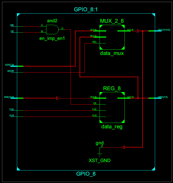
Figure 27 : GPIO port
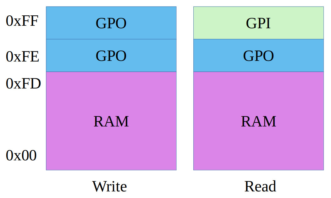
Figure 28 : simpleCPU memory map
To connect this peripheral device to the processor data bus we need to add a DATA MUX: MUX_2_16 i.e. we now have two components wanting to connect to the processor's data-in bus (memory and GPIO). The selection between these two sources is made by the address decoder logic, a seven input AND gate: AND_7. This AND gate is connected to the top seven bits of the address bus, so that when the processor writes to addresses 0xFF, or 0xFE the GPIO's clock enable (CE) line is activated i.e. set to a logic-1. From this new top-level HDL description the Xilinx ISE tools can create an RTL schematic, as shown in figure 29.
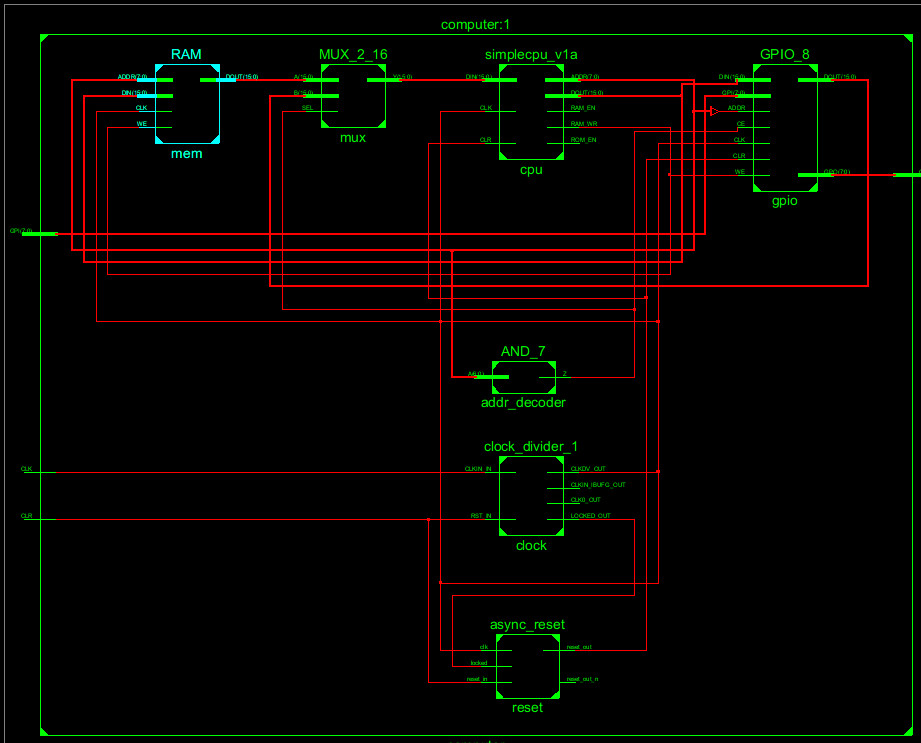
Figure 29 : top level schematic simpleCPU + GPIO + memory
In addition to this GPIO we also need a clock generator and a reset circuit. The clock generator can be implemented using the Xilinx IP-core tools, allowing us to implement a Digital Clock Manager (DCM) i.e. a hardcore component inside the FPGA that can be used to divide an external clock source down to a lower frequency, in this case the external 50MHz clock down to a 10MHz clock. The software tools automatically generate this component, providing an VHDL template that we add to our HDL description, an auto generated RTL schematic symbol of this component is shown in figure 30.
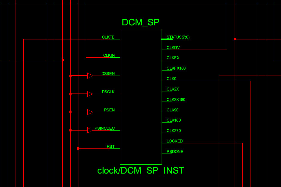
Figure 30 : Digital Clock Manager (DCM)
To ensure that the processor only starts working when the DCM clock is stable and to ensure that contact bounce from the RESET button does not cause the processor to be repeatedly restarted i implemented the async_reset.vhd component below. This component uses the DCM's lock pin to hold the processor in reset until the internal 10MHz clock is stable i.e. locked. The RESET button is debounced by a simple shift register circuit, i confess not the most robust debounce circuit, but it seems to do its job ok :).
-- =============================================================================================================
-- *
-- * Copyright (c) Mike
-- *
-- * File Name: async_reset.vhd
-- *
-- * Version: V1.0
-- *
-- * Release Date:
-- *
-- * Author(s): M.Freeman
-- *
-- * Description: async to syn reset circuit
-- *
-- * Conditions of Use: THIS CODE IS COPYRIGHT AND IS SUPPLIED "AS IS" WITHOUT WARRANTY OF ANY KIND, INCLUDING,
-- *                    BUT NOT LIMITED TO, ANY IMPLIED WARRANTY OF MERCHANTABILITY AND FITNESS FOR A
-- *                    PARTICULAR PURPOSE.
-- *
-- * Notes:
-- *
-- =============================================================================================================

library IEEE;
use IEEE.STD_LOGIC_1164.ALL;

entity async_reset is
Port ( clk         : in  STD_LOGIC;
       locked      : in  STD_LOGIC;
       reset_in    : in  STD_LOGIC;
       reset_out   : out STD_LOGIC;
       reset_out_n : out STD_LOGIC );
end async_reset;

architecture async_reset_arch of async_reset is

    constant SIZE : integer := 4;

    signal reset_internal : std_logic_vector(SIZE downto 0);
    signal full : std_logic_vector(SIZE downto 0);

begin

    full <= (others => '1');

    reset_shift_reg : process ( clk, reset_in )
    begin
        if reset_in = '1'
        then
            reset_internal <= (others =>'0');
        elsif clk='1' and clk'event
        then
            if locked = '1'
            then
                reset_internal(0) <= '1';

                for I in 0 to SIZE-1
                loop
                    reset_internal(SIZE-I) <= reset_internal(SIZE-I-1);
	            end loop;
	         else
	           reset_internal <= (others =>'0');
	         end if;
	     end if;
    end process;


    reset_gen : process( clk )
    begin
        if clk='1' and clk'event
        then
            if reset_internal /= full
            then
                reset_out   <= '1';
                reset_out_n <= '0';
            else
                reset_out   <= '0';
                reset_out_n <= '1';
            end if;
        end if;
    end process;

end async_reset_arch;
The final top-level HDL description is shown below, "wiring" up all of our top level components to produce a final simpleCPUv1a computer.
library IEEE;
use IEEE.STD_LOGIC_1164.ALL;

entity computer is
port(
  CLK : in STD_LOGIC;
  CLR : in STD_LOGIC;
  GPI : in  STD_LOGIC_VECTOR(7 downto 0);
  GPO : out STD_LOGIC_VECTOR(7 downto 0) );
end computer;

architecture computer_arch of computer is

  component clock_divider_1
  port(
    CLKIN_IN        : IN std_logic;
    RST_IN          : IN std_logic;
    CLKDV_OUT       : OUT std_logic;
    CLKIN_IBUFG_OUT : OUT std_logic;
    CLK0_OUT        : OUT std_logic;
    LOCKED_OUT      : OUT std_logic );
  end component;

  component async_reset
  port(
    clk         : in  STD_LOGIC;
    locked      : in  STD_LOGIC;
    reset_in    : in  STD_LOGIC;
    reset_out   : out STD_LOGIC;
    reset_out_n : out STD_LOGIC );
  end component;

  component simplecpu_v1a
  port(
    CLK    : in  STD_LOGIC;
    CLR    : in  STD_LOGIC;
    ROM_EN : out STD_LOGIC;
    RAM_EN : out STD_LOGIC;
    RAM_WR : out STD_LOGIC;
    ADDR   : out STD_LOGIC_VECTOR(7 downto 0);
    DIN    : in  STD_LOGIC_VECTOR(15 downto 0);
    DOUT   : out STD_LOGIC_VECTOR(15 downto 0) );
  end component;

  component RAM
  port (
    CLK  : in  STD_LOGIC;
    WE   : in  STD_LOGIC;
    ADDR : in  STD_LOGIC_VECTOR(7 downto 0);
    DIN  : in  STD_LOGIC_VECTOR(15 downto 0);
    DOUT : out STD_LOGIC_VECTOR(15 downto 0) );
  end component;

  component GPIO_8
  port (
    CLK  : in  STD_LOGIC;
    CLR  : in  STD_LOGIC;
    WE   : in  STD_LOGIC;
    CE   : in  STD_LOGIC;
    ADDR : in  STD_LOGIC;
    DIN  : in  STD_LOGIC_VECTOR(15 downto 0);
    DOUT : out STD_LOGIC_VECTOR(15 downto 0);
    GPI  : in  STD_LOGIC_VECTOR(7 downto 0);
    GPO  : out STD_LOGIC_VECTOR(7 downto 0) );
  end component;

  component MUX_2_16
  port (
    A, B : IN  STD_LOGIC_VECTOR(15 downto 0);
    SEL  : IN  STD_LOGIC;
    Y    : OUT STD_LOGIC_VECTOR(15 downto 0));
  end component;

  component AND_7
  port(
    A : IN STD_LOGIC_VECTOR( 6 downto 0 );
    Z : OUT STD_LOGIC);
  end component;

  signal clk_int   : STD_LOGIC;
  signal clr_int   : STD_LOGIC;
  signal clr_n_int : STD_LOGIC;
  signal locked    : STD_LOGIC;
  signal clk_int_bufg : STD_LOGIC;
  signal clk_int_50MHz : STD_LOGIC;

  signal addr     : STD_LOGIC_VECTOR(7 downto 0);
  signal data_in  : STD_LOGIC_VECTOR(15 downto 0);
  signal data_out : STD_LOGIC_VECTOR(15 downto 0);

  signal mem_data_out : STD_LOGIC_VECTOR(15 downto 0);

  signal gpio_data_out : STD_LOGIC_VECTOR(15 downto 0);
  signal gpio_cs   : STD_LOGIC;

  signal ram_wr   : STD_LOGIC;
  signal row_en   : STD_LOGIC;
  signal ram_en   : STD_LOGIC;

begin

  clock : clock_divider_1 port map(
    CLKIN_IN        => CLK,
    RST_IN          => CLR,
    CLKDV_OUT       => clk_int,
    CLKIN_IBUFG_OUT => clk_int_bufg,
    CLK0_OUT        => clk_int_50MHz,
    LOCKED_OUT      => locked );

  reset : async_reset port map(
    clk         => clk_int,
    locked      => locked,
    reset_in    => CLR,
    reset_out   => clr_int,
    reset_out_n => clr_n_int );

  cpu : simplecpu_v1a port map(
    CLK    => clk_int,
    CLR    => clr_int,
    ROM_EN => row_en,
    RAM_EN => ram_en,
    RAM_WR => ram_wr,
    ADDR   => addr,
    DIN    => data_in,
    DOUT   => data_out );

  mem : RAM port map(
    CLK  => clk_int,
    WE   => ram_wr,
    ADDR => addr,
    DIN  => data_out,
    DOUT => mem_data_out );

  gpio : GPIO_8 port map(
    CLK  => clk_int,
    CLR  => clr_int,
    WE   => ram_wr,
    CE   => gpio_cs,
    ADDR => addr(0),
    DIN  => data_out,
    DOUT => gpio_data_out,
    GPI  => GPI,
    GPO  => GPO );

  addr_decoder : AND_7 port map(
    A => addr(7 downto 1),
    Z => gpio_cs );

  mux : MUX_2_16 port map(
    A   => mem_data_out,
    B   => gpio_data_out,
    SEL => gpio_cs,
    Y   => data_in );

end computer_arch;
To test out this new design the test code below is used. What we have is an incrementing COUNT variable that is written to the output port. We can then look at these 8-bits using a scope, the LSB will have the highest frequency, the MSB the lowest. To integrate the input port into this test code the 8-bit input value is bitwise ANDed with this COUNT variable i.e. if a specific input bit is 0 then that output bit is masked, set to zero. This code is a bit of a cut and paste solution as we do not have an absolute addressing mode bitwise-AND instruction, but it works ok :).
Note, in the Xilinx User Constraints File (UCF) the inputs connected to the IO header are configured to use pull-ups, so these default to a logic-1, the other four input bits are controlled via switches, allowing the user to enable and disable each output bit.
########
# CODE #
########

start:
  load count        # load count variable
  add 1             # inc
  store count       # update
  store tmp

test0:
  load 0xFF         # test input port bits
  and 0x01
  jumpnz test1
  load tmp
  and 0xFE          # 1111 1110
  store tmp

test1:
  load 0xFF
  and 0x02
  jumpnz test2
  load tmp
  and 0xFD          # 1111 1101
  store tmp

test2:
  load 0xFF
  and 0x04
  jumpnz test3
  load tmp
  and 0xFB          # 1111 1011
  store tmp

test3:
  load 0xFF
  and 0x08
  jumpnz test4
  load tmp
  and 0xF7          # 1111 0111
  store tmp

test4:
  load 0xFF
  and 0x10
  jumpnz test5
  load tmp
  and 0xEF          # 1110 1111
  store tmp

test5:
  load 0xFF
  and 0x20
  jumpnz test6
  load tmp
  and 0xDF          # 1101 1111
  store tmp

test6:
  load 0xFF
  and 0x40
  jumpnz test7
  load tmp
  and 0xBF          # 1011 1111
  store tmp

test7:
  load 0xFF
  and 0x80
  jumpnz update
  load tmp
  and 0x7F          # 0111 1111
  store tmp

update:
  load tmp
  store 0xFF        # store to output port
  jump start        # repeat

count:
    .data 0
tmp:
    .data 0
All seems to work Ok, not a complete test, but a reasonable test. The MSB has a period of approx 2.4ms, the LSB has a period of approx 18.6us, as shown in figure 31. You can download copies of these files as a ISE project with testbench here: (Link).
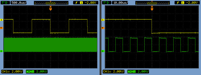
Figure 31 : output signals, MSB (left) and LSB (right)
WORK IN PROGRESS

This work is licensed under a Creative Commons Attribution-NonCommercial-NoDerivatives 4.0 International License.
Contact email: mike@simplecpudesign.com